EP1434360A1 - Synchronisationsschaltung - Google Patents
Synchronisationsschaltung Download PDFInfo
- Publication number
- EP1434360A1 EP1434360A1 EP02406140A EP02406140A EP1434360A1 EP 1434360 A1 EP1434360 A1 EP 1434360A1 EP 02406140 A EP02406140 A EP 02406140A EP 02406140 A EP02406140 A EP 02406140A EP 1434360 A1 EP1434360 A1 EP 1434360A1
- Authority
- EP
- European Patent Office
- Prior art keywords
- feedback
- synchronization circuit
- circuit according
- sequence
- shift register
- Prior art date
- Legal status (The legal status is an assumption and is not a legal conclusion. Google has not performed a legal analysis and makes no representation as to the accuracy of the status listed.)
- Granted
Links
Images
Classifications
-
- H—ELECTRICITY
- H04—ELECTRIC COMMUNICATION TECHNIQUE
- H04B—TRANSMISSION
- H04B1/00—Details of transmission systems, not covered by a single one of groups H04B3/00 - H04B13/00; Details of transmission systems not characterised by the medium used for transmission
- H04B1/69—Spread spectrum techniques
- H04B1/707—Spread spectrum techniques using direct sequence modulation
- H04B1/7073—Synchronisation aspects
- H04B1/7075—Synchronisation aspects with code phase acquisition
-
- G—PHYSICS
- G01—MEASURING; TESTING
- G01S—RADIO DIRECTION-FINDING; RADIO NAVIGATION; DETERMINING DISTANCE OR VELOCITY BY USE OF RADIO WAVES; LOCATING OR PRESENCE-DETECTING BY USE OF THE REFLECTION OR RERADIATION OF RADIO WAVES; ANALOGOUS ARRANGEMENTS USING OTHER WAVES
- G01S19/00—Satellite radio beacon positioning systems; Determining position, velocity or attitude using signals transmitted by such systems
- G01S19/01—Satellite radio beacon positioning systems transmitting time-stamped messages, e.g. GPS [Global Positioning System], GLONASS [Global Orbiting Navigation Satellite System] or GALILEO
- G01S19/13—Receivers
- G01S19/24—Acquisition or tracking or demodulation of signals transmitted by the system
-
- H—ELECTRICITY
- H04—ELECTRIC COMMUNICATION TECHNIQUE
- H04J—MULTIPLEX COMMUNICATION
- H04J13/00—Code division multiplex systems
- H04J13/10—Code generation
Definitions
- the invention relates to a synchronization circuit according to the preamble of claim 1.
- Such synchronization circuits can produce an internal sequence analog values, which one in a received signal coded, repetitions of a basic binary sequence containing external sequence and synchronized with it is used, such as e.g. decoding of signals in communications technology, especially the mobile telephony and with location systems such as GPS is required.
- the invention is based on the object Specify generic synchronization circuit, the one has more favorable synchronization behavior than that known generic synchronization circuits. This task is characterized by the characteristics in the Part of claim 1 solved.
- the synchronization circuit according to the invention generally synchronizes quickly and easily and what crucial in many practical applications Importance is, even under unfavorable conditions like weak signal and strong interference. So could with large negative signal-to-noise ratios satisfactory, sufficient for practical purposes Synchronization behavior can be achieved.
- the synchronization circuit according to the invention is suitable for all applications in which data is CDMA encoded be transmitted. It can be used directly for processing a external signal derived from a received signal can be used if the basic sequence is an m-sequence, however, it is also used in the processing of CDMA-encoded signals possible which other types of Use basic sequences such as Gold episodes or Kasami episodes.
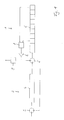
- the synchronization circuit comprises (FIG. 1) an analog feedback shift register 1 and a buffer 2 connected upstream thereof.
- the buffer 2 comprises an adder 3 and a shift register 4 with 1,023 storage locations for analog values.
- the output of the shift register 4 is fed back to the second input of the adder 3.
- the analog feedback shift register 1 comprises an adder 5 and an analog shift register 6 with ten memory locations.
- a feedback circuit 7 is connected to taps at the tenth memory location and one or more additional memory locations. In the example, (4), there is only one additional tap at the third memory location.
- the tapped analog values are linked in the feedback circuit 7 in accordance with a feedback function.
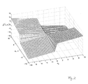
- the graph of a possible feedback function with two arguments f (x 1 , x 2 ) is shown in FIG. 2.
- the output of the feedback circuit 7 is connected to the second input of the adder 5 via a scaler 8.
- the output of the scaler 8 is also a Discriminator 9 connected to a square or a others the input signal in the positive range imaging circuit, a low pass filter and one Contains threshold detector and emits a binary signal.
- the discriminator can also be anywhere else of the shift register 6, the feedback circuit 7, the Scaler 8 and the adder 5 formed loop be connected.
- the input signal is a digital signal certain bit width, e.g. 12 bits for the amount and one additional bit for the sign, before.
- the values can represented as floating point numbers or as whole numbers become. However, they will be used to differentiate from binary values are referred to as analog values.
- the Input signal contains a binary sequence, which is represented by a binary feedback shift register can be generated that has the same feedback pattern as the analog one feedback shift register 1, i.e. in the case shown a feedback pattern in which the new value is given by Link is generated according to (4). But it can be very be very noisy with a typical signal-to-noise ratio from e.g. -35dB.
- the analog values of the input signal which elements of a Forming the input sequence first reach buffer 2.
- the basic sequence stored in buffer 2 now becomes Generation of an external sequence read out repeatedly and on the input of the analog feedback shift register 1 directed. Since the basic sequence by linking to the Data bit can be inverted, two analog feedback shift registers are used, the one is fed the external sequence via an inverter becomes.
- the analog feedback shift register 1 which receives a favorable sequence, ie one which contains a portion which is as similar as possible to the coded basic sequence p 1 , ..., p 1'023 , should now be an internal sequence a 1 , .. ., generate a 1'023 , which should also coincide with the external sequence with regard to the phase position.
- the external sequence corresponds to repetitions of the basic sequence, which contains the noisy basic sequence p 1 , ..., p 1'023 .
- the feedback function should work in every sector certain values of the sign of the arguments is defined essentially a linear combination of the arguments.
- the resulting discontinuities in the Sector boundaries can be steadied or smoothed out it has been shown that deviations tend to behavior deteriorate and should therefore not be large.
- the amount of the feedback value should be slightly less than 1, preferably between 0.90 and 0.99. It is favorable if the feedback function supplies a value of 1 for arguments of the amount 1, ie (5)
- 1 for
- 1, applies and the function value is then multiplied by a selectable factor k ⁇ 1, in particular 0.90 ⁇ k ⁇ 0.99. This multiplication is carried out by the adjustable scaler 8, which is connected downstream of the feedback circuit 7 evaluating the feedback function.
- x 1 , ..., x m each have the amount 1, ie can also be viewed as binary quantities, the two properties mentioned lead to f (x 1 , ..., x m ) of the combination x 1 ⁇ ... corresponds to mx m .
- the feedback function f is invariant by swapping the arguments. As a function of each individual argument, i.e. if the the rest, it should be antisymmetric and monotone.
- this function is ensures that (5) is satisfied, one in each sector Linear combination of arguments with coefficients of +1 or -1.
- Feedback function can be adjusted accordingly. Also can be the factor k, depending on the implementation as fixed or variable size, integrated in the feedback function be what e.g. require an adaptation of condition (5) would.
- the synchronization circuit Since the synchronization circuit works with stored data thanks to the buffer 2, its operating speed is independent of the chip rate of the received signal and can be significantly higher.
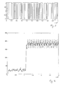
- the criterion for successful synchronization is the power of the internal sequence generated, which is taken off at the output of the scaler 8. While the elements of the internal sequence have approximately the same value as those of the external sequence before a synchronization, the latter is amplified by a factor 1 / (1-k), that is usually between 10 and 100, when synchronization has taken place.
- the performance of the internal sequence (a i ) accordingly rises sharply, as shown in FIG. 4.
- the discriminator 9 in which the power is determined by squaring and filtering is smoothed by a low-pass filter and averaged over a longer period of time and finally the result is compared with a threshold value. It emits a corresponding binary signal that indicates the synchronization that has taken place.
- the lack of synchronization can be random, e.g. a particularly unfavorable form of Are due to an unfavorable phase position of the received signal or an unfavorable Sampling time before a data bit change, which leads to that in the buffer 2 (Fig. 1) adds copies of sequences in which the one containing the basic sequence sought Proportion with different signs occurs, which leads to a serious weakening of the said portion can lead to the noise component. In such cases it is it makes sense to fill buffer 2 with a new basic sequence and restart the synchronization process with it.
- the mentioned components of the synchronization circuit must by no means available as separate components.
- the Shift registers can e.g. each from a corresponding Memory with linear addressing and a write and a read pointer are formed.
Landscapes
- Engineering & Computer Science (AREA)
- Computer Networks & Wireless Communication (AREA)
- Radar, Positioning & Navigation (AREA)
- Remote Sensing (AREA)
- Signal Processing (AREA)
- Physics & Mathematics (AREA)
- General Physics & Mathematics (AREA)
- Synchronisation In Digital Transmission Systems (AREA)
- Analogue/Digital Conversion (AREA)
- Stabilization Of Oscillater, Synchronisation, Frequency Synthesizers (AREA)
- Image Analysis (AREA)
- Time-Division Multiplex Systems (AREA)
Abstract
Description
- Fig. 1
- eine erfindungsgemässe Synchronisationsschaltung,
- Fig. 2
- den Graphen der bei der erfindungsgemässen Synchronisationsschaltung verwendeten Rückkopplungsfunktion,
- Fig. 3
- einen Ausschnitt aus einer möglichen Grundfolge und
- Fig. 4
- die Entwicklung der Leistung eines Rückkopplungssignals in der erfindungsgemässen Synchronisationsschaltung während einer Synchronisation.
| b2\b1 | 0 | 1 |
| 0 | 0 | 1 |
| 1 | 1 | 0 |
| p2\p1 | -1 | 1 |
| - 1 | -1 | 1 |
| 1 | 1 | -1 |
- 1
- analoges rückgekoppeltes Schieberegister
- 2
- Puffer
- 3
- Addierer
- 4
- Schieberegister
- 5
- Addierer
- 6
- Schieberegister
- 7
- Rückkopplungsschaltung
- 8
- Skalierer
- 9
- Diskriminator
Claims (11)
- Synchronisationsschaltung zur Verarbeitung einer von einer Eingangsfolge abgeleiteten externen Folge analoger Werte, mit einem analogen rückgekoppelten Schieberegister (1), in welchem nach einem bestimmten Rückkopplungsmuster in Speicherplätzen eines Schieberegisters (6) gespeicherte analoge Werte zur Ableitung eines Rückkopplungswertes gemäss einer Rückkopplungsfunktion verknüpft werden, aus dem durch Ueberlagerung mit einem neuen Glied der externen Folge ein neuer Eingangswert erzeugt wird, der dem Eingang des Schieberegisters (6) zugeführt wird, dadurch gekennzeichnet, dass die Rückkopplungsfunktion im wesentlichen innerhalb eines jeden durch bestimmte Werte der Vorzeichen der Argumente gekennzeichneten Sektors im wesentlichen eine Linearkombination der Argumente ist.
- Synchronisationsschaltung nach Anspruch 1, dadurch gekennzeichnet, dass der Betrag der Rückkopplungsfunktion 1 ist, wenn die Beträge der Argumente jeweils 1 sind.
- Synchronisationsschaltung nach Anspruch 1 oder 2, dadurch gekennzeichnet, dass das Vorzeichen der Rückkopplungsfunktion stets dem Vorzeichen der Verknüpfung der Argumente entspricht.
- Synchronisationsschaltung nach einem der Ansprüche 1 bis 3, dadurch gekennzeichnet, dass die Rückkopplungsfunktion invariant unter Vertauschung der Argumente ist.
- Synchronisationsschaltung nach einem der Ansprüche 1 bis 4, dadurch gekennzeichnet, dass die Rückkopplungsfunktion als Funktion eines jeden Argumentes antisymmetrisch und monoton ist.
- Synchronisationsschaltung nach Anspruch 1, dadurch gekennzeichnet, dass der Betrag der Rückkopplungsfunktion im wesentlichen dem Mittelwert der Beträge der Argumente entspricht.
- Synchronisationsschaltung nach einem der Ansprüche 1 bis 6, dadurch gekennzeichnet, dass der Rückkopplungswert durch Multiplikation des Wertes der Rückkopplungsfunktion mit einem Faktor k<1, der vorzugsweise zwischen 0,90 und 0,99 liegt, hergestellt wird.
- Synchronisationsschaltung nach einem der Ansprüche 1 bis 7, dadurch gekennzeichnet, dass sie eine Rückkopplungsschaltung (7) zur Auswertung der Rückkopplungsfunktion und einen Skalierer (8) zur Multiplikation ihres Ausgangswertes mit einem Faktor sowie einen Addierer (5) zur Ueberlagerung des Rückkopplungswertes mit dem neuen Glied der externen Folge umfasst.
- Synchronisationsschaltung nach Anspruch 8, dadurch gekennzeichnet, dass sie einen Diskriminator (9) zur Erzeugung eines erfolgte Synchronisation anzeigenden binären Ausgangssignals umfasst, dessen Eingang mit dem Ausgang der Rückkopplungsschaltung (7) verbunden ist und der vorzugsweise einen Quadrierer oder eine andere ein Eingangssignal in den positiven Bereich abbildende Schaltung, einen Tiefpassfilter und einen Schwellwertdetektor umfasst.
- Synchronisationsschaltung nach einem der Ansprüche 1 bis 9, dadurch gekennzeichnet, dass sie einen dem analogen rückgekoppelten Schieberegister (1) vorgeschalteten Puffer (2) zur Aufaddierung aufeinanderfolgender, jeweils eine Grundfolge enthaltender Abschnitte einer Eingangsfolge zur Herstellung der externen Folge aufweist.
- Synchronisationsschaltung nach Anspruch 10, dadurch gekennzeichnet, dass, das der Puffer ein Schieberegister (4) umfasst sowie einen demselben vorgeschalteten Addierer (3) zur Addition eines Gliedes der Eingangsfolge zu einem Ausgangswert des Schieberegisters (4).
Priority Applications (5)
| Application Number | Priority Date | Filing Date | Title |
|---|---|---|---|
| ES02406140T ES2263758T3 (es) | 2002-12-24 | 2002-12-24 | Circuito de sincronizacion. |
| EP02406140A EP1434360B1 (de) | 2002-12-24 | 2002-12-24 | Synchronisationsschaltung |
| AT02406140T ATE327597T1 (de) | 2002-12-24 | 2002-12-24 | Synchronisationsschaltung |
| DE50206925T DE50206925D1 (de) | 2002-12-24 | 2002-12-24 | Synchronisationsschaltung |
| US10/618,051 US7218698B2 (en) | 2002-12-24 | 2003-07-14 | Synchronization circuit |
Applications Claiming Priority (1)
| Application Number | Priority Date | Filing Date | Title |
|---|---|---|---|
| EP02406140A EP1434360B1 (de) | 2002-12-24 | 2002-12-24 | Synchronisationsschaltung |
Publications (2)
| Publication Number | Publication Date |
|---|---|
| EP1434360A1 true EP1434360A1 (de) | 2004-06-30 |
| EP1434360B1 EP1434360B1 (de) | 2006-05-24 |
Family
ID=32405829
Family Applications (1)
| Application Number | Title | Priority Date | Filing Date |
|---|---|---|---|
| EP02406140A Expired - Lifetime EP1434360B1 (de) | 2002-12-24 | 2002-12-24 | Synchronisationsschaltung |
Country Status (5)
| Country | Link |
|---|---|
| US (1) | US7218698B2 (de) |
| EP (1) | EP1434360B1 (de) |
| AT (1) | ATE327597T1 (de) |
| DE (1) | DE50206925D1 (de) |
| ES (1) | ES2263758T3 (de) |
Families Citing this family (1)
| Publication number | Priority date | Publication date | Assignee | Title |
|---|---|---|---|---|
| JP5013040B2 (ja) * | 2005-09-29 | 2012-08-29 | 株式会社メガチップス | 動き探索方法 |
Citations (2)
| Publication number | Priority date | Publication date | Assignee | Title |
|---|---|---|---|---|
| US5737360A (en) * | 1995-06-19 | 1998-04-07 | International Business Machines, Corp. | System employing continuous-time dissipative pseudorandom dynamics for communications and measurement |
| WO2001037441A2 (en) * | 1999-11-15 | 2001-05-25 | Massachusetts Institute Of Technology | A nonlinear dynamic system for spread spectrum code generation and acquisition |
Family Cites Families (3)
| Publication number | Priority date | Publication date | Assignee | Title |
|---|---|---|---|---|
| SE503920C2 (sv) * | 1994-10-03 | 1996-09-30 | Ericsson Telefon Ab L M | Sätt att synkronisera signaler och anordning härför |
| US5612973A (en) * | 1995-06-19 | 1997-03-18 | Massachusetts Institute Of Technology | System employing dissipative pseudorandom dynamics for communications and measurement |
| US6724805B1 (en) * | 1999-11-15 | 2004-04-20 | Massachusetts Institute Of Technology | Nonlinear dynamic system for spread spectrum code generation and acquisition |
-
2002
- 2002-12-24 DE DE50206925T patent/DE50206925D1/de not_active Expired - Lifetime
- 2002-12-24 ES ES02406140T patent/ES2263758T3/es not_active Expired - Lifetime
- 2002-12-24 AT AT02406140T patent/ATE327597T1/de active
- 2002-12-24 EP EP02406140A patent/EP1434360B1/de not_active Expired - Lifetime
-
2003
- 2003-07-14 US US10/618,051 patent/US7218698B2/en not_active Expired - Lifetime
Patent Citations (2)
| Publication number | Priority date | Publication date | Assignee | Title |
|---|---|---|---|---|
| US5737360A (en) * | 1995-06-19 | 1998-04-07 | International Business Machines, Corp. | System employing continuous-time dissipative pseudorandom dynamics for communications and measurement |
| WO2001037441A2 (en) * | 1999-11-15 | 2001-05-25 | Massachusetts Institute Of Technology | A nonlinear dynamic system for spread spectrum code generation and acquisition |
Non-Patent Citations (1)
| Title |
|---|
| VIGODA BENJAMIN: "A Nonlinear Dynamic System for Spread Spectrum Code Acquisition", MASTERS THESIS; MIT MEDIA LAB, 9 August 1999 (1999-08-09), Boston, US, pages 1 - 90, XP002167577, Retrieved from the Internet <URL:www.media.mit.edu/physics/publications/theses/99.06.vigoda.pdf> [retrieved on 20010516] * |
Also Published As
| Publication number | Publication date |
|---|---|
| US20040120440A1 (en) | 2004-06-24 |
| ES2263758T3 (es) | 2006-12-16 |
| EP1434360B1 (de) | 2006-05-24 |
| DE50206925D1 (de) | 2006-06-29 |
| ATE327597T1 (de) | 2006-06-15 |
| US7218698B2 (en) | 2007-05-15 |
Similar Documents
| Publication | Publication Date | Title |
|---|---|---|
| DE2652245C2 (de) | Verfahren zur Beseitigung von Nebenmaxima eines von einem Radarempfänger aufgefangenen und komprimierten Radar-Echoimpulses | |
| DE69723451T2 (de) | Deformation eines digitalen bildes mit effizienter berechnung | |
| DE3233288C2 (de) | ||
| CH643410A5 (de) | Filterschaltung mit einer biquadratischen uebertragungsfunktion. | |
| DE4310347C2 (de) | Verfahren und Schaltkreis zum Erstellen von Zickzackadressen | |
| DE10236898A1 (de) | Videofiltern mit verbesserter Spur unter Verwendung von Wavelet-Entrauschungstechniken | |
| DE2906265A1 (de) | Doppelueberlagerungs-fm-tuner | |
| DE2503107A1 (de) | Korrekturcode fuer impulsfehler | |
| DE10146582A1 (de) | Vorrichtung und Verfahren zur Teilbandzerlegung von Bildsignalen | |
| DE69026373T2 (de) | Filterkreis für digitale Signale | |
| EP0016318B1 (de) | Korrekturschaltung zur Verbesserung der Konturenschärfe von Fernsehbildern | |
| DE2634426A1 (de) | Bandkompressionseinrichtung | |
| DE2947072C2 (de) | (b + a)-Bit-D/A-Wandler mit b-Bit- Hilfs-D/A-Wandler | |
| DE1562215A1 (de) | Variabler Entzerrer | |
| DE3044582A1 (de) | Digitaler verstaerker, insbesondere zur verwendung in einer digitalen fernsprech-teilnehmerschaltung | |
| EP1434360B1 (de) | Synchronisationsschaltung | |
| EP1246452B1 (de) | Verfahren und Vorrichtung zur Versteilerung von Signalübergängen bei Fernsehbildern | |
| Hof | Gründungsfinanzierung | |
| DE69018233T2 (de) | Bildverarbeitungssystem zur Wiedergabe von mit Kleinbildern überlagerten Grossbildern. | |
| DE3147171A1 (de) | Signalpegeldetektorschaltung | |
| DE102005018858A1 (de) | Digitales Filter und Verfahren zur Bestimmung seiner Koeffizienten | |
| EP0148528B1 (de) | Verfahren und Schaltungsanordnung zum Erhöhen der Auflösung eines digitalisierten, zeitabhängigen Signals | |
| DE4203413C2 (de) | Mehrfachabtastungsverfahren | |
| DE10302234A1 (de) | Flexibler Dezimator | |
| DE69609241T2 (de) | Vorrichtung zur einstellbaren Verzögerung eines analogen Signals und entsprechende einstellbare akustische Antenne |
Legal Events
| Date | Code | Title | Description |
|---|---|---|---|
| PUAI | Public reference made under article 153(3) epc to a published international application that has entered the european phase |
Free format text: ORIGINAL CODE: 0009012 |
|
| 17P | Request for examination filed |
Effective date: 20040122 |
|
| AK | Designated contracting states |
Kind code of ref document: A1 Designated state(s): AT BE BG CH CY CZ DE DK EE ES FI FR GB GR IE IT LI LU MC NL PT SE SI SK TR |
|
| AX | Request for extension of the european patent |
Extension state: AL LT LV MK RO |
|
| 17Q | First examination report despatched |
Effective date: 20050127 |
|
| AKX | Designation fees paid |
Designated state(s): AT BE BG CH CY CZ DE DK EE ES FI FR GB GR IE IT LI LU MC NL PT SE SI SK TR |
|
| GRAP | Despatch of communication of intention to grant a patent |
Free format text: ORIGINAL CODE: EPIDOSNIGR1 |
|
| GRAS | Grant fee paid |
Free format text: ORIGINAL CODE: EPIDOSNIGR3 |
|
| GRAA | (expected) grant |
Free format text: ORIGINAL CODE: 0009210 |
|
| AK | Designated contracting states |
Kind code of ref document: B1 Designated state(s): AT BE BG CH CY CZ DE DK EE ES FI FR GB GR IE IT LI LU MC NL PT SE SI SK TR |
|
| PG25 | Lapsed in a contracting state [announced via postgrant information from national office to epo] |
Ref country code: SI Free format text: LAPSE BECAUSE OF FAILURE TO SUBMIT A TRANSLATION OF THE DESCRIPTION OR TO PAY THE FEE WITHIN THE PRESCRIBED TIME-LIMIT Effective date: 20060524 Ref country code: CZ Free format text: LAPSE BECAUSE OF FAILURE TO SUBMIT A TRANSLATION OF THE DESCRIPTION OR TO PAY THE FEE WITHIN THE PRESCRIBED TIME-LIMIT Effective date: 20060524 Ref country code: NL Free format text: LAPSE BECAUSE OF FAILURE TO SUBMIT A TRANSLATION OF THE DESCRIPTION OR TO PAY THE FEE WITHIN THE PRESCRIBED TIME-LIMIT Effective date: 20060524 Ref country code: SK Free format text: LAPSE BECAUSE OF FAILURE TO SUBMIT A TRANSLATION OF THE DESCRIPTION OR TO PAY THE FEE WITHIN THE PRESCRIBED TIME-LIMIT Effective date: 20060524 |
|
| REG | Reference to a national code |
Ref country code: GB Ref legal event code: FG4D Free format text: NOT ENGLISH |
|
| REG | Reference to a national code |
Ref country code: CH Ref legal event code: EP |
|
| REG | Reference to a national code |
Ref country code: IE Ref legal event code: FG4D Free format text: LANGUAGE OF EP DOCUMENT: GERMAN |
|
| REF | Corresponds to: |
Ref document number: 50206925 Country of ref document: DE Date of ref document: 20060629 Kind code of ref document: P |
|
| REG | Reference to a national code |
Ref country code: CH Ref legal event code: NV Representative=s name: ZIMMERLI, WAGNER & PARTNER AG |
|
| PG25 | Lapsed in a contracting state [announced via postgrant information from national office to epo] |
Ref country code: DK Free format text: LAPSE BECAUSE OF FAILURE TO SUBMIT A TRANSLATION OF THE DESCRIPTION OR TO PAY THE FEE WITHIN THE PRESCRIBED TIME-LIMIT Effective date: 20060824 |
|
| GBT | Gb: translation of ep patent filed (gb section 77(6)(a)/1977) |
Effective date: 20060816 |
|
| REG | Reference to a national code |
Ref country code: SE Ref legal event code: TRGR |
|
| PG25 | Lapsed in a contracting state [announced via postgrant information from national office to epo] |
Ref country code: PT Free format text: LAPSE BECAUSE OF FAILURE TO SUBMIT A TRANSLATION OF THE DESCRIPTION OR TO PAY THE FEE WITHIN THE PRESCRIBED TIME-LIMIT Effective date: 20061024 |
|
| NLV1 | Nl: lapsed or annulled due to failure to fulfill the requirements of art. 29p and 29m of the patents act | ||
| REG | Reference to a national code |
Ref country code: ES Ref legal event code: FG2A Ref document number: 2263758 Country of ref document: ES Kind code of ref document: T3 |
|
| ET | Fr: translation filed | ||
| PG25 | Lapsed in a contracting state [announced via postgrant information from national office to epo] |
Ref country code: MC Free format text: LAPSE BECAUSE OF NON-PAYMENT OF DUE FEES Effective date: 20061231 |
|
| PLBE | No opposition filed within time limit |
Free format text: ORIGINAL CODE: 0009261 |
|
| STAA | Information on the status of an ep patent application or granted ep patent |
Free format text: STATUS: NO OPPOSITION FILED WITHIN TIME LIMIT |
|
| 26N | No opposition filed |
Effective date: 20070227 |
|
| PG25 | Lapsed in a contracting state [announced via postgrant information from national office to epo] |
Ref country code: GR Free format text: LAPSE BECAUSE OF FAILURE TO SUBMIT A TRANSLATION OF THE DESCRIPTION OR TO PAY THE FEE WITHIN THE PRESCRIBED TIME-LIMIT Effective date: 20060825 |
|
| PG25 | Lapsed in a contracting state [announced via postgrant information from national office to epo] |
Ref country code: BG Free format text: LAPSE BECAUSE OF FAILURE TO SUBMIT A TRANSLATION OF THE DESCRIPTION OR TO PAY THE FEE WITHIN THE PRESCRIBED TIME-LIMIT Effective date: 20060824 Ref country code: EE Free format text: LAPSE BECAUSE OF FAILURE TO SUBMIT A TRANSLATION OF THE DESCRIPTION OR TO PAY THE FEE WITHIN THE PRESCRIBED TIME-LIMIT Effective date: 20060524 |
|
| PG25 | Lapsed in a contracting state [announced via postgrant information from national office to epo] |
Ref country code: LU Free format text: LAPSE BECAUSE OF NON-PAYMENT OF DUE FEES Effective date: 20061224 Ref country code: TR Free format text: LAPSE BECAUSE OF FAILURE TO SUBMIT A TRANSLATION OF THE DESCRIPTION OR TO PAY THE FEE WITHIN THE PRESCRIBED TIME-LIMIT Effective date: 20060524 |
|
| PG25 | Lapsed in a contracting state [announced via postgrant information from national office to epo] |
Ref country code: CY Free format text: LAPSE BECAUSE OF FAILURE TO SUBMIT A TRANSLATION OF THE DESCRIPTION OR TO PAY THE FEE WITHIN THE PRESCRIBED TIME-LIMIT Effective date: 20060524 |
|
| REG | Reference to a national code |
Ref country code: CH Ref legal event code: PFA Owner name: U-BLOX AG Free format text: U-BLOX AG#ZUERCHERSTRASSE 68#8800 THALWIL (CH) -TRANSFER TO- U-BLOX AG#ZUERCHERSTRASSE 68#8800 THALWIL (CH) |
|
| REG | Reference to a national code |
Ref country code: CH Ref legal event code: NV Representative=s name: WAGNER PATENT AG, CH |
|
| PGFP | Annual fee paid to national office [announced via postgrant information from national office to epo] |
Ref country code: CH Payment date: 20141219 Year of fee payment: 13 Ref country code: ES Payment date: 20141226 Year of fee payment: 13 Ref country code: SE Payment date: 20141219 Year of fee payment: 13 Ref country code: IE Payment date: 20141222 Year of fee payment: 13 Ref country code: FI Payment date: 20141211 Year of fee payment: 13 |
|
| PGFP | Annual fee paid to national office [announced via postgrant information from national office to epo] |
Ref country code: AT Payment date: 20141222 Year of fee payment: 13 |
|
| PGFP | Annual fee paid to national office [announced via postgrant information from national office to epo] |
Ref country code: IT Payment date: 20141219 Year of fee payment: 13 |
|
| PGFP | Annual fee paid to national office [announced via postgrant information from national office to epo] |
Ref country code: BE Payment date: 20141219 Year of fee payment: 13 |
|
| REG | Reference to a national code |
Ref country code: FR Ref legal event code: PLFP Year of fee payment: 14 |
|
| PG25 | Lapsed in a contracting state [announced via postgrant information from national office to epo] |
Ref country code: BE Free format text: LAPSE BECAUSE OF NON-PAYMENT OF DUE FEES Effective date: 20151231 |
|
| REG | Reference to a national code |
Ref country code: CH Ref legal event code: PL |
|
| REG | Reference to a national code |
Ref country code: SE Ref legal event code: EUG |
|
| REG | Reference to a national code |
Ref country code: AT Ref legal event code: MM01 Ref document number: 327597 Country of ref document: AT Kind code of ref document: T Effective date: 20151224 |
|
| PG25 | Lapsed in a contracting state [announced via postgrant information from national office to epo] |
Ref country code: SE Free format text: LAPSE BECAUSE OF NON-PAYMENT OF DUE FEES Effective date: 20151225 |
|
| REG | Reference to a national code |
Ref country code: IE Ref legal event code: MM4A |
|
| PG25 | Lapsed in a contracting state [announced via postgrant information from national office to epo] |
Ref country code: CH Free format text: LAPSE BECAUSE OF NON-PAYMENT OF DUE FEES Effective date: 20151231 Ref country code: IE Free format text: LAPSE BECAUSE OF NON-PAYMENT OF DUE FEES Effective date: 20151224 Ref country code: LI Free format text: LAPSE BECAUSE OF NON-PAYMENT OF DUE FEES Effective date: 20151231 |
|
| PG25 | Lapsed in a contracting state [announced via postgrant information from national office to epo] |
Ref country code: AT Free format text: LAPSE BECAUSE OF NON-PAYMENT OF DUE FEES Effective date: 20151224 |
|
| REG | Reference to a national code |
Ref country code: FR Ref legal event code: PLFP Year of fee payment: 15 |
|
| PG25 | Lapsed in a contracting state [announced via postgrant information from national office to epo] |
Ref country code: IT Free format text: LAPSE BECAUSE OF NON-PAYMENT OF DUE FEES Effective date: 20151224 |
|
| REG | Reference to a national code |
Ref country code: ES Ref legal event code: FD2A Effective date: 20170203 |
|
| PG25 | Lapsed in a contracting state [announced via postgrant information from national office to epo] |
Ref country code: ES Free format text: LAPSE BECAUSE OF NON-PAYMENT OF DUE FEES Effective date: 20151225 |
|
| PG25 | Lapsed in a contracting state [announced via postgrant information from national office to epo] |
Ref country code: FI Free format text: LAPSE BECAUSE OF NON-PAYMENT OF DUE FEES Effective date: 20151224 |
|
| REG | Reference to a national code |
Ref country code: FR Ref legal event code: PLFP Year of fee payment: 16 |
|
| PGFP | Annual fee paid to national office [announced via postgrant information from national office to epo] |
Ref country code: DE Payment date: 20191210 Year of fee payment: 18 |
|
| PGFP | Annual fee paid to national office [announced via postgrant information from national office to epo] |
Ref country code: FR Payment date: 20191219 Year of fee payment: 18 |
|
| PGFP | Annual fee paid to national office [announced via postgrant information from national office to epo] |
Ref country code: GB Payment date: 20191220 Year of fee payment: 18 |
|
| REG | Reference to a national code |
Ref country code: DE Ref legal event code: R119 Ref document number: 50206925 Country of ref document: DE |
|
| GBPC | Gb: european patent ceased through non-payment of renewal fee |
Effective date: 20201224 |
|
| PG25 | Lapsed in a contracting state [announced via postgrant information from national office to epo] |
Ref country code: FR Free format text: LAPSE BECAUSE OF NON-PAYMENT OF DUE FEES Effective date: 20201231 |
|
| PG25 | Lapsed in a contracting state [announced via postgrant information from national office to epo] |
Ref country code: GB Free format text: LAPSE BECAUSE OF NON-PAYMENT OF DUE FEES Effective date: 20201224 Ref country code: DE Free format text: LAPSE BECAUSE OF NON-PAYMENT OF DUE FEES Effective date: 20210701 |