EP1434340A2 - Isolierte Niederspannungsversorgung - Google Patents
Isolierte Niederspannungsversorgung Download PDFInfo
- Publication number
- EP1434340A2 EP1434340A2 EP03300277A EP03300277A EP1434340A2 EP 1434340 A2 EP1434340 A2 EP 1434340A2 EP 03300277 A EP03300277 A EP 03300277A EP 03300277 A EP03300277 A EP 03300277A EP 1434340 A2 EP1434340 A2 EP 1434340A2
- Authority
- EP
- European Patent Office
- Prior art keywords
- bridge
- capacitor
- voltage
- circuit
- circuit according
- Prior art date
- Legal status (The legal status is an assumption and is not a legal conclusion. Google has not performed a legal analysis and makes no representation as to the accuracy of the status listed.)
- Granted
Links
Images

Classifications
-
- H—ELECTRICITY
- H02—GENERATION; CONVERSION OR DISTRIBUTION OF ELECTRIC POWER
- H02M—APPARATUS FOR CONVERSION BETWEEN AC AND AC, BETWEEN AC AND DC, OR BETWEEN DC AND DC, AND FOR USE WITH MAINS OR SIMILAR POWER SUPPLY SYSTEMS; CONVERSION OF DC OR AC INPUT POWER INTO SURGE OUTPUT POWER; CONTROL OR REGULATION THEREOF
- H02M5/00—Conversion of AC power input into AC power output, e.g. for change of voltage, for change of frequency, for change of number of phases
- H02M5/02—Conversion of AC power input into AC power output, e.g. for change of voltage, for change of frequency, for change of number of phases without intermediate conversion into DC
- H02M5/04—Conversion of AC power input into AC power output, e.g. for change of voltage, for change of frequency, for change of number of phases without intermediate conversion into DC by static converters
- H02M5/22—Conversion of AC power input into AC power output, e.g. for change of voltage, for change of frequency, for change of number of phases without intermediate conversion into DC by static converters using discharge tubes with control electrode or semiconductor devices with control electrode
- H02M5/25—Conversion of AC power input into AC power output, e.g. for change of voltage, for change of frequency, for change of number of phases without intermediate conversion into DC by static converters using discharge tubes with control electrode or semiconductor devices with control electrode using devices of a thyratron or thyristor type requiring extinguishing means
- H02M5/257—Conversion of AC power input into AC power output, e.g. for change of voltage, for change of frequency, for change of number of phases without intermediate conversion into DC by static converters using discharge tubes with control electrode or semiconductor devices with control electrode using devices of a thyratron or thyristor type requiring extinguishing means using semiconductor devices only
-
- H—ELECTRICITY
- H02—GENERATION; CONVERSION OR DISTRIBUTION OF ELECTRIC POWER
- H02M—APPARATUS FOR CONVERSION BETWEEN AC AND AC, BETWEEN AC AND DC, OR BETWEEN DC AND DC, AND FOR USE WITH MAINS OR SIMILAR POWER SUPPLY SYSTEMS; CONVERSION OF DC OR AC INPUT POWER INTO SURGE OUTPUT POWER; CONTROL OR REGULATION THEREOF
- H02M7/00—Conversion of AC power input into DC power output; Conversion of DC power input into AC power output
- H02M7/02—Conversion of AC power input into DC power output without possibility of reversal
- H02M7/04—Conversion of AC power input into DC power output without possibility of reversal by static converters
- H02M7/12—Conversion of AC power input into DC power output without possibility of reversal by static converters using discharge tubes with control electrode or semiconductor devices with control electrode
- H02M7/145—Conversion of AC power input into DC power output without possibility of reversal by static converters using discharge tubes with control electrode or semiconductor devices with control electrode using devices of a thyratron or thyristor type requiring extinguishing means
- H02M7/155—Conversion of AC power input into DC power output without possibility of reversal by static converters using discharge tubes with control electrode or semiconductor devices with control electrode using devices of a thyratron or thyristor type requiring extinguishing means using semiconductor devices only
- H02M7/1555—Conversion of AC power input into DC power output without possibility of reversal by static converters using discharge tubes with control electrode or semiconductor devices with control electrode using devices of a thyratron or thyristor type requiring extinguishing means using semiconductor devices only with control circuit
-
- H—ELECTRICITY
- H02—GENERATION; CONVERSION OR DISTRIBUTION OF ELECTRIC POWER
- H02M—APPARATUS FOR CONVERSION BETWEEN AC AND AC, BETWEEN AC AND DC, OR BETWEEN DC AND DC, AND FOR USE WITH MAINS OR SIMILAR POWER SUPPLY SYSTEMS; CONVERSION OF DC OR AC INPUT POWER INTO SURGE OUTPUT POWER; CONTROL OR REGULATION THEREOF
- H02M1/00—Details of apparatus for conversion
- H02M1/0003—Details of control, feedback or regulation circuits
- H02M1/0006—Arrangements for supplying an adequate voltage to the control circuit of converters
Definitions
- the present invention relates to the provision of a relatively low DC supply voltage to a circuit for controlling a switch or a load supplied by a relatively high tension.
- the invention relates more particularly the supply of a load control circuit high voltage upstream of a rectifier bridge, for example, supplying a rectified voltage to a converter switching power supply type.
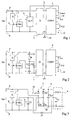
- Figure 1 shows, very schematically and in the form of blocks, a first classic example of supply a relatively low supply voltage to a circuit 1 control, in this example via a switch K, of a load 2 (Q) supplied by an alternating voltage relatively high Vac applied between terminals P and N.
- the terminals P and N correspond to alternative input terminals a double-wave rectification bridge 3, including rectified output terminals E and M supply a converter power 4 (CONV), for example of the switching power supply type.
- CONV converter power 4
- the converter 4 provides several DC voltages of different levels (for example, two voltages Vs1 and Vs2) referenced to a mass G which can be different from the output mass M of bridge 3.
- the supply voltage of the control circuit 1 is, for example, supplied by a power supply unit 6 itself supplied from a voltage Vsaux supplied by the converter 4 by means of an auxiliary winding.
- the auxiliary winding alters the coupling and increases the leakage inductances of the converter.
- Figure 2 shows a second classic example for supplying a supply voltage to a circuit 1 of control of a load 2 supplied by an alternating voltage Vac.
- a 4 ′ switching power supply type converter The essential difference from figure 1 is that the example of figure 2 uses a high voltage capacity CX upstream of the righting bridge 3 rather than a winding auxiliary converter 4 '.
- CX capacity is connected by one of its electrodes in phase P of the alternative power supply and by the other of these electrodes to a resistance R in series with a diode D and a capacitor C for supplying the supply voltage of circuit 1.
- a Zener diode DZ is connected between the midpoint of the serial association of the resistance R with diode D and neutral N of the power supply alternative.
- the Zener DZ diode fixes the value of the aux terminals of capacitor C, therefore of low voltage power supply for circuit 1.
- Diode D serves as a rectification, the capacitor C being charged alternately on two of the alternating voltage Vac, since the diode DZ leads directly via the CX capacitor.
- the present invention aims to propose a new solution for supplying a relatively low voltage to a control circuit of a load supplied by a voltage relatively high, generally alternative, which overcomes the disadvantages of known solutions.
- the invention aims more particularly at avoiding the use of a auxiliary winding specific to the converter and to be resolved isolation problems, while taking energy supply of the control circuit 1, placed upstream of the bridge recovery, downstream of the latter.
- the invention also aims to avoid the use of a high impedance upstream of the righting bridge.
- the second capacitor charges during a conduction period of the bridge where that of its elements rectification which connects the first respective electrodes of the capacitors leads, this element connecting the electrodes of most negative potential.
- the first capacitor is a low supply capacitor voltage of a circuit downstream of the bridge.
- the circuit includes a second high voltage diode, the anode is connected, via a switch logic control, at the second electrode of the first capacitor, and whose cathode is connected to an input terminal control circuit logic upstream of the bridge.
- the righting bridge is a full wave bridge or phase.
- the bridge is a mixed or controlled bridge.
- said charge consists of at least one of the elements of bridge straightening.
- the first capacitor is charged by an auxiliary winding of a transformer of a switching power supply downstream of the bridge.
- a feature of the present invention is to use a capacitor storing a relatively voltage bass downstream of the full wave rectifier bridge or three-phase to supply a capacitor, arranged upstream of the righting bridge and intended to supply power to the low voltage isolated control circuit. According to the invention, these two capacitors are connected by a high voltage diode providing isolation.
- Another feature of the present invention is to use one of the diodes (or more generally one of the rectifying elements) of the full-wave or three-phase bridge to close the charging circuit of the capacitor placed in upstream of the bridge.
- the invention uses this element of straightening integrated in the bridge, in direct conduction only when driving to transfer energy to destination of the power converter downstream from the bridge.
- FIG 3 shows schematically and under block form, an embodiment of an isolated circuit low voltage power supply 10 according to the present invention.
- This circuit 10 is intended to supply a supply voltage V a control circuit 1 (CTRL) of a high load 2 (Q) voltage.
- CTRL control circuit 1
- circuit 1 controls a switch K placed in series with load 2 between two terminals P and N of application of an alternating voltage Vac.
- a bridge of double alternation rectification 3 has its alternative inputs connected to terminals P and N and provides rectified high voltage to a 4 'CONV converter of the switching power supply type in a similar way to the classic example in Figure 2.
- a high voltage CHT capacitor has been shown in E and M terminals of rectified output of bridge 3. This capacitor CHT is used to store the converter supply voltage.
- bridge 3 is made up of four diodes D1 to D4, the diodes D1 and D3 being in series between the terminals E and M as well as the diodes D2 and D4.
- the anodes of diodes D1 and D2 are connected respectively to terminals P and N.
- the capacitors C1 and C2 are both low voltage capacitors.
- the diode Dr plays the role of insulation barrier on the second electrodes (positive) capacitors while a diode (here D4) of bridge 3 acts as an isolation barrier between the first capacitor electrodes (ground).
- the invention takes advantage of the presence in deck 3 diode D4. However, it is not used as in its normal operation within the bridge. Indeed, for the charge of the high voltage capacitor CHT between terminals E and M, we use for arbitrarily positive half-waves diodes D1 and D4 live and for negative halfwaves diodes D2 and D3 also while these are polarized live.
- the capacitor C2 for supplying the relatively low voltage V is charged only by direct transfer of energy from capacitor C1 by balancing the respective charges of the capacitors C1 and C2.
- the only condition on deck 3 is that this load balance takes place during the periods when the diode D4 conducts, that is to say in this example during the capacitor charge periods CHT on positive half-waves.
- this diode D4 is then not used for transfer energy in its direct direction.
- the diode D4 when the diode D4 conducts, the voltage at its terminals decreases and tends towards its junction voltage (for example of the order of 0.6 volts). So if the voltage across the capacitor C2 is less than the voltage across the capacitor C1, the diode Dr becomes conductive and the voltages across capacitors C2 and C1 are balanced. Indeed, the voltage drops in the diodes D4 and Dr compensate for so that the voltage V across the capacitor C2 corresponds at the voltage across the capacitor C1. In fact, the meaning of diodes Dr and D4 makes it the capacitor C1 which recharges the capacitor C2. In fact, the current ensuring the charge of the capacitor C2 subtracts from the current corresponding to the transfer of energy to the 4 'converter for its operation.
- capacitor C1 is dimensioned according to the application to continuously supply sufficient voltage.
- the capacitor C1 downstream of the bridge 3 corresponds to a capacitor used to supply a circuit control unit (not shown) of converter 2 (for example, the control circuit of the switching switch of this converter).
- the present invention takes advantage the existence of a low voltage capacitor downstream from the bridge to use the energy it stores in order to transfer this energy on the capacitor C2 upstream of the bridge.
- An advantage of the present invention is that it does not no additional auxiliary winding isolated by compared to the other windings of the 4 ′ converter.
- the coupling of the transformer supplying low voltages by the converter is therefore improved compared to the case where one of the windings must be referenced to neutral of the power supply alternative.
- the invention uses one of the existing windings (for example, the one supplying the supply voltage of the converter control circuit).
- Another advantage of the invention is that it does not no high voltage capacitor required, either upstream or downstream from the righting bridge.
- Another advantage of the invention is that its implementation work does not require, compared to a conventional circuit of the type from that of FIG. 2, that a slight oversizing of the capacitor C1 supplying the circuit of the switch to cutting to take account of the supply voltage necessary for circuit 1 upstream of the righting bridge.
- the diode Dr is a high voltage diode to respect the need for isolation, the diode D4 being it necessarily a high voltage diode insofar as it is already integrated in the bridge.
- FIG. 4 represents an alternative embodiment of the invention.
- This variant consists in adding to a circuit of the type described in relation to FIG. 3, a logical information transfer circuit between downstream of the bridge rectifier and control circuit 1 supplied by the capacitor C2.
- the circuit 1 control was intended to open a switch K supplying, by the capacitor C2, the trigger of a triac T in series with load 2 between terminals P and N.
- a resistance Rk (possibly confused with the switch K), is interposed between the latter and the trigger of the triac T.
- control circuit receives a logic setpoint LOG from a logic circuit 11 (MCU) of downstream of the righting bridge 3.
- MCU logic circuit 11
- circuit 11 is a microcontroller of which an output transistor B is mounted at open collector with its transmitter connected to the positive electrode of capacitor C1 and its base controlled by circuit 11 (of a not shown).
- the collector of transistor B or any equivalent element providing a logical level is linked, via an isolation di Di, at the input of the circuit 1 receiving the LOG signal, which is also connected to earth (neutral N of the alternative power supply) by a capacitor C3 in parallel with a resistor Ri.
- the role of capacitor C3 is to temporarily store the command state of the logic signal, the resistance Ri being there to make disappear this signal after a certain time (time constant defined by components C3 and Ri).
- the logical instruction is not transmitted from downstream to upstream of the bridge rectifier only when diode D4 conducts and the insulation between the upstream and downstream parts of the righting bridge is guaranteed, for the control signal, by diodes Di and D4.
- An advantage of the embodiment of Figure 4 is that it makes it possible to transfer an order instruction simply by adding a high voltage di di between downstream and upstream a rectifying bridge supplying a converter.
- FIG. 5 schematically represents and partial, another embodiment of the invention according to which the load to be controlled is precisely the rectifier bridge 13.
- the load to be controlled is precisely the rectifier bridge 13.
- it is a mixed bridge in which, for example compared to the previous figures, the diodes D3 and D4 have been replaced by two thyristors Th3 and Th4 with cathode trigger.
- the capacitor C1 is used to supply energy to circuits 11 (CT3) and 11 '(CT4) for thyristor control respectively Th3 and Th4, via two capacitors C2 and C2 'having an identical operation to the one described in the previous figures for the capacitor C2.
- CT3 circuits 11
- C2 ' is associated with a diode Dr, Dr' connected downstream of bridge 13 on the positive electrode of the capacitor C1.
- the circuits 11 and 11 ' are supplied by the respective voltages across capacitors C2 and C2 '.
- Such an embodiment allows power to be generated necessary to control thyristors of the composite bridge.
- the present invention is capable of various variations and modifications that will appear to humans art.
- the dimensions given to the different capacitors and in particular the low voltage capacitor (s) specific to the invention depend on the application and the expected consumption of control circuits.
- the invention has been described in connection with the exploitation a supply capacitor (C1) for the control circuit the switching switch of a power converter, this applies more generally as soon as one can have a low voltage source downstream of the rectifier bridge and that you want to order, with isolation or references from different voltage, a switch in the bridge or upstream of this one.
- the circuit adaptations for such operation are at the reach of the skilled person.
Landscapes
- Engineering & Computer Science (AREA)
- Power Engineering (AREA)
- Rectifiers (AREA)
Applications Claiming Priority (2)
| Application Number | Priority Date | Filing Date | Title |
|---|---|---|---|
| FR0216806 | 2002-12-27 | ||
| FR0216806A FR2849551A1 (fr) | 2002-12-27 | 2002-12-27 | Alimentation basse tension isolee |
Publications (3)
| Publication Number | Publication Date |
|---|---|
| EP1434340A2 true EP1434340A2 (de) | 2004-06-30 |
| EP1434340A3 EP1434340A3 (de) | 2005-11-02 |
| EP1434340B1 EP1434340B1 (de) | 2007-08-01 |
Family
ID=32406546
Family Applications (1)
| Application Number | Title | Priority Date | Filing Date |
|---|---|---|---|
| EP03300277A Expired - Lifetime EP1434340B1 (de) | 2002-12-27 | 2003-12-22 | Isolierte Niederspannungsversorgung |
Country Status (5)
| Country | Link |
|---|---|
| US (1) | US7072197B2 (de) |
| EP (1) | EP1434340B1 (de) |
| JP (1) | JP2004215498A (de) |
| DE (1) | DE60315248D1 (de) |
| FR (1) | FR2849551A1 (de) |
Families Citing this family (2)
| Publication number | Priority date | Publication date | Assignee | Title |
|---|---|---|---|---|
| US8598737B2 (en) | 2010-12-13 | 2013-12-03 | Light-Based Technologies Incorporated | Synchronous switching power supply |
| CN115599615B (zh) * | 2022-10-20 | 2023-07-04 | 长沙方维科技有限公司 | Cht技术处理器电源管理设计架构 |
Family Cites Families (4)
| Publication number | Priority date | Publication date | Assignee | Title |
|---|---|---|---|---|
| AT403103B (de) * | 1994-12-12 | 1997-11-25 | Siemens Ag Oesterreich | Netzgleichrichterschaltung |
| US6018472A (en) * | 1998-04-06 | 2000-01-25 | Intel Corporation | Method and apparatus for power factor correction |
| FR2783981B1 (fr) * | 1998-09-29 | 2000-12-08 | St Microelectronics Sa | Circuit de commande d'une charge a alimenter par une tension alternative |
| JP2001006890A (ja) * | 1999-06-21 | 2001-01-12 | Koito Mfg Co Ltd | 放電灯点灯回路 |
-
2002
- 2002-12-27 FR FR0216806A patent/FR2849551A1/fr not_active Withdrawn
-
2003
- 2003-12-22 DE DE60315248T patent/DE60315248D1/de not_active Expired - Lifetime
- 2003-12-22 EP EP03300277A patent/EP1434340B1/de not_active Expired - Lifetime
- 2003-12-24 JP JP2003427179A patent/JP2004215498A/ja not_active Abandoned
- 2003-12-29 US US10/747,969 patent/US7072197B2/en not_active Expired - Lifetime
Also Published As
| Publication number | Publication date |
|---|---|
| EP1434340B1 (de) | 2007-08-01 |
| US20040141344A1 (en) | 2004-07-22 |
| FR2849551A1 (fr) | 2004-07-02 |
| JP2004215498A (ja) | 2004-07-29 |
| EP1434340A3 (de) | 2005-11-02 |
| DE60315248D1 (de) | 2007-09-13 |
| US7072197B2 (en) | 2006-07-04 |
Similar Documents
| Publication | Publication Date | Title |
|---|---|---|
| EP3109988A1 (de) | Leistungswandler mit korrekturschaltkreis des leistungsfaktors | |
| FR3034924A1 (fr) | Convertisseur alternatif-continu a limitation du courant d'appel | |
| EP3010133B1 (de) | Anordnung zur kontrollierten gleichrichtung | |
| EP1368884A2 (de) | Kommutierungshilfsschaltung für ein schaltnetzteil | |
| EP0820141B1 (de) | Nullspannungsansteuerung einer hybriden Brückenschaltung | |
| EP0433144B1 (de) | Netzteil vom Typ AC-DC-Wandler | |
| EP3051681A1 (de) | Begrenzungsschaltkreis für den einschaltstrom | |
| EP0798838B1 (de) | Schaltung zur Verbesserung des Leistungsfaktors mit doppelter Entladung | |
| FR2936113A1 (fr) | Dispositif convertisseur et alimentation sans interruption equipee d'un tel dispositif | |
| EP0567408B1 (de) | Einrichtung zum Betrieb von Entladungslampen und Fahrzeugscheinwerfer mit solch einer Einrichtung | |
| EP3345456B1 (de) | Elektronischer wandler und beleuchtungssystem mit solch einem wandler | |
| EP0772280A1 (de) | Gleichgerichtete Doppelspannungsversorgungskreis | |
| EP1434340B1 (de) | Isolierte Niederspannungsversorgung | |
| FR2859580A1 (fr) | Gradateur pour charges resistives ou capacitives | |
| EP0967842B1 (de) | Sollwertsendung über ein Wechselstromversorgungsnetz | |
| EP3965299B1 (de) | Vorrichtung zur steuerung eines thyristors | |
| EP0743742B1 (de) | Leistungsfaktorverbesserung für eine gleichgerichtete Leistungsversorgung | |
| EP1493522B1 (de) | Funkenerosionsmaschine | |
| FR2778286A1 (fr) | Circuit convertisseur de tension | |
| FR3087596A1 (fr) | Systeme electrique et procede de charge d'une batterie, notamment pour vehicule | |
| EP0107539A1 (de) | Steuerschaltung für einen Synchronmotor mit zwei Ankerwicklungen | |
| EP1324478A2 (de) | Hochspannungswandler mit schneller Antwortzeit | |
| FR2730104A1 (fr) | Alimentation continue a correcteur de facteur de puissance et convertisseur a decoupage utilisable dans une telle alimentation | |
| FR2698499A1 (fr) | Circuit pour faire fonctionner une charge inductive. | |
| EP1073190A1 (de) | Nichtisolierter Wechselstrom-Gleichstromwandler |
Legal Events
| Date | Code | Title | Description |
|---|---|---|---|
| PUAI | Public reference made under article 153(3) epc to a published international application that has entered the european phase |
Free format text: ORIGINAL CODE: 0009012 |
|
| AK | Designated contracting states |
Kind code of ref document: A2 Designated state(s): AT BE BG CH CY CZ DE DK EE ES FI FR GB GR HU IE IT LI LU MC NL PT RO SE SI SK TR |
|
| AX | Request for extension of the european patent |
Extension state: AL LT LV MK |
|
| PUAL | Search report despatched |
Free format text: ORIGINAL CODE: 0009013 |
|
| AK | Designated contracting states |
Kind code of ref document: A3 Designated state(s): AT BE BG CH CY CZ DE DK EE ES FI FR GB GR HU IE IT LI LU MC NL PT RO SE SI SK TR |
|
| AX | Request for extension of the european patent |
Extension state: AL LT LV MK |
|
| RIC1 | Information provided on ipc code assigned before grant |
Ipc: 7H 02M 7/04 B Ipc: 7H 02M 5/22 B Ipc: 7H 02M 1/08 B Ipc: 7H 02M 5/42 A Ipc: 7H 02M 5/257 B |
|
| 17P | Request for examination filed |
Effective date: 20060421 |
|
| AKX | Designation fees paid |
Designated state(s): DE FR GB IT |
|
| GRAP | Despatch of communication of intention to grant a patent |
Free format text: ORIGINAL CODE: EPIDOSNIGR1 |
|
| GRAJ | Information related to disapproval of communication of intention to grant by the applicant or resumption of examination proceedings by the epo deleted |
Free format text: ORIGINAL CODE: EPIDOSDIGR1 |
|
| GRAP | Despatch of communication of intention to grant a patent |
Free format text: ORIGINAL CODE: EPIDOSNIGR1 |
|
| GRAS | Grant fee paid |
Free format text: ORIGINAL CODE: EPIDOSNIGR3 |
|
| GRAA | (expected) grant |
Free format text: ORIGINAL CODE: 0009210 |
|
| AK | Designated contracting states |
Kind code of ref document: B1 Designated state(s): DE FR GB IT |
|
| REG | Reference to a national code |
Ref country code: GB Ref legal event code: FG4D Free format text: NOT ENGLISH |
|
| REF | Corresponds to: |
Ref document number: 60315248 Country of ref document: DE Date of ref document: 20070913 Kind code of ref document: P |
|
| GBT | Gb: translation of ep patent filed (gb section 77(6)(a)/1977) |
Effective date: 20071003 |
|
| PGFP | Annual fee paid to national office [announced via postgrant information from national office to epo] |
Ref country code: GB Payment date: 20071129 Year of fee payment: 5 |
|
| PLBE | No opposition filed within time limit |
Free format text: ORIGINAL CODE: 0009261 |
|
| STAA | Information on the status of an ep patent application or granted ep patent |
Free format text: STATUS: NO OPPOSITION FILED WITHIN TIME LIMIT |
|
| 26N | No opposition filed |
Effective date: 20080506 |
|
| PG25 | Lapsed in a contracting state [announced via postgrant information from national office to epo] |
Ref country code: DE Free format text: LAPSE BECAUSE OF FAILURE TO SUBMIT A TRANSLATION OF THE DESCRIPTION OR TO PAY THE FEE WITHIN THE PRESCRIBED TIME-LIMIT Effective date: 20071103 |
|
| PGFP | Annual fee paid to national office [announced via postgrant information from national office to epo] |
Ref country code: FR Payment date: 20071228 Year of fee payment: 5 |
|
| GBPC | Gb: european patent ceased through non-payment of renewal fee |
Effective date: 20081222 |
|
| REG | Reference to a national code |
Ref country code: FR Ref legal event code: ST Effective date: 20090831 |
|
| PG25 | Lapsed in a contracting state [announced via postgrant information from national office to epo] |
Ref country code: GB Free format text: LAPSE BECAUSE OF NON-PAYMENT OF DUE FEES Effective date: 20081222 |
|
| PG25 | Lapsed in a contracting state [announced via postgrant information from national office to epo] |
Ref country code: FR Free format text: LAPSE BECAUSE OF NON-PAYMENT OF DUE FEES Effective date: 20081231 |
|
| PG25 | Lapsed in a contracting state [announced via postgrant information from national office to epo] |
Ref country code: IT Free format text: LAPSE BECAUSE OF NON-PAYMENT OF DUE FEES Effective date: 20071231 |