EP1434260A2 - Method to manufacture LDMOS transistors - Google Patents
Method to manufacture LDMOS transistors Download PDFInfo
- Publication number
- EP1434260A2 EP1434260A2 EP03104373A EP03104373A EP1434260A2 EP 1434260 A2 EP1434260 A2 EP 1434260A2 EP 03104373 A EP03104373 A EP 03104373A EP 03104373 A EP03104373 A EP 03104373A EP 1434260 A2 EP1434260 A2 EP 1434260A2
- Authority
- EP
- European Patent Office
- Prior art keywords
- forming
- semiconductor
- photoresist layer
- patterned photoresist
- species
- Prior art date
- Legal status (The legal status is an assumption and is not a legal conclusion. Google has not performed a legal analysis and makes no representation as to the accuracy of the status listed.)
- Granted
Links
Images
Classifications
-
- H—ELECTRICITY
- H10—SEMICONDUCTOR DEVICES; ELECTRIC SOLID-STATE DEVICES NOT OTHERWISE PROVIDED FOR
- H10P—GENERIC PROCESSES OR APPARATUS FOR THE MANUFACTURE OR TREATMENT OF DEVICES COVERED BY CLASS H10
- H10P30/00—Ion implantation into wafers, substrates or parts of devices
- H10P30/20—Ion implantation into wafers, substrates or parts of devices into semiconductor materials, e.g. for doping
- H10P30/22—Ion implantation into wafers, substrates or parts of devices into semiconductor materials, e.g. for doping using masks
-
- H—ELECTRICITY
- H10—SEMICONDUCTOR DEVICES; ELECTRIC SOLID-STATE DEVICES NOT OTHERWISE PROVIDED FOR
- H10D—INORGANIC ELECTRIC SEMICONDUCTOR DEVICES
- H10D30/00—Field-effect transistors [FET]
- H10D30/01—Manufacture or treatment
- H10D30/021—Manufacture or treatment of FETs having insulated gates [IGFET]
- H10D30/028—Manufacture or treatment of FETs having insulated gates [IGFET] of double-diffused metal oxide semiconductor [DMOS] FETs
- H10D30/0281—Manufacture or treatment of FETs having insulated gates [IGFET] of double-diffused metal oxide semiconductor [DMOS] FETs of lateral DMOS [LDMOS] FETs
-
- H—ELECTRICITY
- H10—SEMICONDUCTOR DEVICES; ELECTRIC SOLID-STATE DEVICES NOT OTHERWISE PROVIDED FOR
- H10D—INORGANIC ELECTRIC SEMICONDUCTOR DEVICES
- H10D30/00—Field-effect transistors [FET]
- H10D30/60—Insulated-gate field-effect transistors [IGFET]
- H10D30/64—Double-diffused metal-oxide semiconductor [DMOS] FETs
- H10D30/65—Lateral DMOS [LDMOS] FETs
-
- H—ELECTRICITY
- H10—SEMICONDUCTOR DEVICES; ELECTRIC SOLID-STATE DEVICES NOT OTHERWISE PROVIDED FOR
- H10D—INORGANIC ELECTRIC SEMICONDUCTOR DEVICES
- H10D62/00—Semiconductor bodies, or regions thereof, of devices having potential barriers
- H10D62/10—Shapes, relative sizes or dispositions of the regions of the semiconductor bodies; Shapes of the semiconductor bodies
- H10D62/17—Semiconductor regions connected to electrodes not carrying current to be rectified, amplified or switched, e.g. channel regions
- H10D62/393—Body regions of DMOS transistors or IGBTs
-
- H—ELECTRICITY
- H10—SEMICONDUCTOR DEVICES; ELECTRIC SOLID-STATE DEVICES NOT OTHERWISE PROVIDED FOR
- H10D—INORGANIC ELECTRIC SEMICONDUCTOR DEVICES
- H10D64/00—Electrodes of devices having potential barriers
- H10D64/20—Electrodes characterised by their shapes, relative sizes or dispositions
- H10D64/27—Electrodes not carrying the current to be rectified, amplified, oscillated or switched, e.g. gates
- H10D64/311—Gate electrodes for field-effect devices
- H10D64/411—Gate electrodes for field-effect devices for FETs
- H10D64/511—Gate electrodes for field-effect devices for FETs for IGFETs
- H10D64/514—Gate electrodes for field-effect devices for FETs for IGFETs characterised by the insulating layers
- H10D64/516—Gate electrodes for field-effect devices for FETs for IGFETs characterised by the insulating layers the thicknesses being non-uniform
-
- H—ELECTRICITY
- H10—SEMICONDUCTOR DEVICES; ELECTRIC SOLID-STATE DEVICES NOT OTHERWISE PROVIDED FOR
- H10P—GENERIC PROCESSES OR APPARATUS FOR THE MANUFACTURE OR TREATMENT OF DEVICES COVERED BY CLASS H10
- H10P30/00—Ion implantation into wafers, substrates or parts of devices
- H10P30/20—Ion implantation into wafers, substrates or parts of devices into semiconductor materials, e.g. for doping
- H10P30/202—Ion implantation into wafers, substrates or parts of devices into semiconductor materials, e.g. for doping characterised by the semiconductor materials
- H10P30/204—Ion implantation into wafers, substrates or parts of devices into semiconductor materials, e.g. for doping characterised by the semiconductor materials into Group IV semiconductors
-
- H—ELECTRICITY
- H10—SEMICONDUCTOR DEVICES; ELECTRIC SOLID-STATE DEVICES NOT OTHERWISE PROVIDED FOR
- H10P—GENERIC PROCESSES OR APPARATUS FOR THE MANUFACTURE OR TREATMENT OF DEVICES COVERED BY CLASS H10
- H10P30/00—Ion implantation into wafers, substrates or parts of devices
- H10P30/20—Ion implantation into wafers, substrates or parts of devices into semiconductor materials, e.g. for doping
- H10P30/21—Ion implantation into wafers, substrates or parts of devices into semiconductor materials, e.g. for doping of electrically active species
- H10P30/212—Through-implantation
-
- H—ELECTRICITY
- H10—SEMICONDUCTOR DEVICES; ELECTRIC SOLID-STATE DEVICES NOT OTHERWISE PROVIDED FOR
- H10P—GENERIC PROCESSES OR APPARATUS FOR THE MANUFACTURE OR TREATMENT OF DEVICES COVERED BY CLASS H10
- H10P30/00—Ion implantation into wafers, substrates or parts of devices
- H10P30/20—Ion implantation into wafers, substrates or parts of devices into semiconductor materials, e.g. for doping
- H10P30/28—Ion implantation into wafers, substrates or parts of devices into semiconductor materials, e.g. for doping characterised by an annealing step, e.g. for activation of dopants
Definitions
- the present invention relates to a method for forming a lateral double diffused metal oxide semiconductor transistor using multiple ion implantation processes.
- LDMOS transistors are used in integrated circuits for high voltage applications. High voltage applications require that the LDMOS transistors have a low on resistance, a high off resistance, and a large electrical safe operating area. To increase the current handling capability of the LDMOS transistors on an integrated circuit a number of LDMOS transistors are often tied together. With the LDMOS transistors connected in parallel the current flow will be shared among the various LDMOS transistors.
- One scheme for forming multiple LDMOS transistors involves forming a multi-fingered structure. To ensure the proper distribution of current among the transistors in a multi-fingered structure it is important that the threshold voltages of the individual LDMOS transistor structures be closely matched.
- the threshold voltage of the LDMOS transistor is set by the multiple ion implantation processes used to form the transistor channel region. During this multiple ion implantation process a patterned photoresist masking layer is formed over the substrate and the dopant species implanted through patterned openings formed in the photoresist masking layer.
- a major limitation to obtaining closely matched threshold voltages is the variation in the resist angle of the various openings through which the dopants are implanted.
- the instant invention is a method for forming multi-fingered LDMOS transistors with closely matched threshold voltages.
- the instant invention is a method for forming a LDMOS with improved threshold voltage.
- the improvement in the threshold comes from a tightly controlled double diffused junction formation process.
- the method comprises forming an epitaxial layer on a semiconductor substrate.
- a deep n-well region is formed in the epitaxial region in which the LDMOS transistor will be formed.
- the double diffused region is formed by first forming a patterned photoresist layer over the deep n-well region with the patterned photoresist layer comprises at least one opening.
- Light implant specie such as boron is implanted into the deep n-well region.
- a hard bake process is then performed and heavy implant specie such as arsenic is then implanted through the opening and into the deep n-well region.
- the hard bake process comprises heating said patterned photoresist layer to temperatures between 75°C and 200°C.
- forming the LOCOS isolation structures comprises performing thermal oxidation processes at temperatures greater than 800°C.
- an epitaxial layer 20 is formed on a semiconductor substrate 10.
- the epitaxial layer 20 can be formed using known semiconductor manufacturing methods. The formation of an epitaxial layer on a semiconductor substrate is optional and the method of the instant invention can be used to form devices on any suitable semiconductor substrate.
- a pad oxide layer 40 is formed on the epitaxial layer 20. The pad oxide layer 40 is necessary to reduce the damage caused by the subsequent implantation processes. For the case where no epitaxial layer is formed the pad oxide layer will be formed on the surface of the semiconductor substrate 10.
- an oppositely doped deep well region 30 is formed in the epitaxial layer 30.
- the deep well region 30 will be n-type.
- an n-type epitaxial layer 20 will require the formation of a p-type deep well region 30.
- an n-type deep well region is formed in a p-type epitaxial layer or a p-type semiconductor substrate.
- a patterned photoresist layer 50 is formed over the pad oxide layer 40.
- the patterned photoresist layer will be on the order of 1.8 ⁇ m to 4 ⁇ m thick.
- the photoresist layer 50 will be 2 ⁇ m to 3 ⁇ m thick.
- Illustrated in Figure 1(a) is a patterned photoresist layer 50 with a single opening that will be used to form a LDMOS transistor with a single finger.
- the method of the instant invention should not be limited to photoresist layers with a single opening. If LDMOS transistors with multiple fingers are required then the deep n-well region 30 and patterned photoresist layer 50 shown in Figure 1(a) can be repeated multiple times along a line in the epitaxial layer 20.
- a blanket layer of photoresist is first formed.
- the photoresist layer is formed using Sumitomo PFI-37 photoresist.
- a soft bake of the photoresist is performed.
- the soft bake process comprises a 75°C to 160°C heat treatment of the blanket layer of photoresist for 60 to 200 seconds.
- the blanket layer of photoresist is exposed.
- a post exposure bake can be performed and in an embodiment the post exposure bake comprises annealing the photoresist layer at temperatures between 60°C to 210°C.
- the photoresist layer is developed to form the opening 55 shown in Figure 1(a).
- Boron species are then implanted through the opening 55 and into the deep well region 30 using multiple ion implantation processes to form the p-type regions 60 and 70 in the deep well region 30 as shown in Figure 1(a).
- the deep p-type region 60 can be formed by implanting a boron containing species at energies of 300KeV to 500Kev and doses of 5 x 10 13 cm -2 to 5 x 10 14 cm -2 .
- the shallower p-type region 70 can also be formed by implanting a boron containing species but at reduced energies of 40KeV to 60KeV and doses of 5 x 10 12 cm -2 to 5 X 10 13 cm -2 .
- the multiple ion implantations of the boron species used to form regions 60 and 70 can be performed in the same implant tool in a continuous sequence or chain process.
- a hard bake process is applied to the patterned photoresist layer 50.
- a hard bake process comprises thermally annealing the patterned photoresist layer 50.
- the hard bake process comprises heating the patterned resist layer 50 to temperatures of 75°C to 200°C for 60 to 200 seconds.
- the hard bake process improves the stability of the patterned photoresist layer 50 to effectively withstand the high power and damage of the arsenic implant.
- arsenic species are implanted through the opening 55 to form the n-type region 80. It should be noted that performing the hard bake process after the multiple boron implantation processes is an important aspect of the instant invention.
- the angle 57 that the edge of the patterned photoresist layer 50 makes with the surface pad oxide layer 40 is reduced. The reduction in the angle 57 leads to penetration of high-energy boron species (i.e.
- the p-type regions 60 and 70 be formed by implanting high-energy boron species before any photoresist hard bake process is performed.
- any light mass implant specie can be implanted before any hard bake photoresist process is performed.
- light mass specie refers to elements in the periodic table below the element silicon.
- any heavy implant specie can be implanted using the hard baked photoresist as a mask.
- heavy implant specie refers to elements in the periodic table above the element silicon.
- LOCOS local oxide isolation structures
- the isolation regions 90 are formed as shown in Figure 1(b).
- LOCOS local oxide isolation structures
- the patterned silicon nitride layers are formed in those areas where no LOCOS isolation structures 90 are desired.
- the LOCOS structures 90 are formed using thermal oxidation.
- the patterned silicon nitride layers will block the oxidation process in those regions of the epitaxial layer 20 that underlie the layers.
- the thermal oxidation process used to form the LOCOS structures 90 takes place at temperatures above 800°C.
- the implanted boron and arsenic species will diffuse forming the double diffused regions 65, 75, and 85 shown in Figure 1(b).
- the boron species have a temperature dependent intrinsic diffusivity constant that is almost an order of magnitude greater than that of the arsenic species and so the lateral diffusion of the boron species that occurs during the LOCOS oxidation process will be greater than that of the arsenic species.
- the difference in lateral diffusion of the boron and arsenic species that occurs during LOCOS oxidation results in the formation of the double diffused regions 65, 75, and 85.
- the thermal annealing required to form the double diffused regions 65, 75, and 85 occur during the LOCOS formation process.
- an independent thermal annealing cycle or cycles
- the temperature of the thermal annealing cycle (or cycles) should be between 800°C and 1200°C.
- the n-type diffused region 85 will form the source of the transistor and the inversion channel of the transistor will be formed in the p-type diffused regions 65 and 75.
- a patterned photoresist layer 100 is formed and used as an ion implantation mask during the implantation of suitable n-type dopant species to form the n-type regions 110 and 115 that function as the drain regions of the LDMOS transistor. During this implantation process n-type dopant species are also implanted into the source region 85 to further increase the n-doping concentration.
- a gate dielectric layer 120 is formed above the double diffused regions 65, 75, and 85.
- the gate dielectric layer comprises silicon oxide but nitrogen containing silicon oxide materials can also be used to form the dielectric layer 120.
- the doped polysilicon structures 130 and 135 can be formed using known processing methods and function as the gate electrodes for the LDMOS transistors 140 and 150 respectively. Therefore the single finger structure illustrated in Figure 1(c) results in the formation of two LDMOS transistors 140 and 150.
- the LDMOS transistors 140 and 150 share a common source region 85.
- the LDMOS transistor 140 also comprises the gate electrode region 130 and the drain region 110.
- the LDMOS transistor 150 also comprises the gate electrode 135 and the drain region 115.
Landscapes
- Insulated Gate Type Field-Effect Transistor (AREA)
Abstract
Description
- The present invention relates to a method for forming a lateral double diffused metal oxide semiconductor transistor using multiple ion implantation processes.
- Lateral double-diffused metal oxide semiconductor (LDMOS) transistors are used in integrated circuits for high voltage applications. High voltage applications require that the LDMOS transistors have a low on resistance, a high off resistance, and a large electrical safe operating area. To increase the current handling capability of the LDMOS transistors on an integrated circuit a number of LDMOS transistors are often tied together. With the LDMOS transistors connected in parallel the current flow will be shared among the various LDMOS transistors. One scheme for forming multiple LDMOS transistors involves forming a multi-fingered structure. To ensure the proper distribution of current among the transistors in a multi-fingered structure it is important that the threshold voltages of the individual LDMOS transistor structures be closely matched. The threshold voltage of the LDMOS transistor is set by the multiple ion implantation processes used to form the transistor channel region. During this multiple ion implantation process a patterned photoresist masking layer is formed over the substrate and the dopant species implanted through patterned openings formed in the photoresist masking layer. In forming the multi-fingered LDMOS transistors required for high current applications a major limitation to obtaining closely matched threshold voltages is the variation in the resist angle of the various openings through which the dopants are implanted. The instant invention is a method for forming multi-fingered LDMOS transistors with closely matched threshold voltages.
- The instant invention is a method for forming a LDMOS with improved threshold voltage. The improvement in the threshold comes from a tightly controlled double diffused junction formation process. In particular the method comprises forming an epitaxial layer on a semiconductor substrate. A deep n-well region is formed in the epitaxial region in which the LDMOS transistor will be formed. The double diffused region is formed by first forming a patterned photoresist layer over the deep n-well region with the patterned photoresist layer comprises at least one opening. Light implant specie such as boron is implanted into the deep n-well region. A hard bake process is then performed and heavy implant specie such as arsenic is then implanted through the opening and into the deep n-well region. During the subsequent formation of the LOCOS isolation structures in the deep n-well region the heavy and light implant specie will diffuse at different rates resulting in the formation of the double diffused region. A dielectric layer is then formed on the epitaxial layer and a LDMOS transistor gate structure formed on the dielectric layer. Drain regions are then formed in the epitaxial layer to complete the LDMOS transistor formation. In an embodiment of the instant invention the hard bake process comprises heating said patterned photoresist layer to temperatures between 75°C and 200°C. In a further embodiment of the instant invention forming the LOCOS isolation structures comprises performing thermal oxidation processes at temperatures greater than 800°C.
- For a more complete understanding of the present invention and the advantages thereof, reference is now made to the following description taken in conjunction with the accompanying drawings, wherein like reference numerals represent like features, in which:
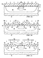
- FIGUREs 1(a) - 1(c) are cross-sectional diagrams showing an embodiment of the instant invention.
-
- Referring to Figure 1(a) an
epitaxial layer 20 is formed on asemiconductor substrate 10. Theepitaxial layer 20 can be formed using known semiconductor manufacturing methods. The formation of an epitaxial layer on a semiconductor substrate is optional and the method of the instant invention can be used to form devices on any suitable semiconductor substrate. Following the formation of the epitaxial layer, apad oxide layer 40 is formed on theepitaxial layer 20. Thepad oxide layer 40 is necessary to reduce the damage caused by the subsequent implantation processes. For the case where no epitaxial layer is formed the pad oxide layer will be formed on the surface of thesemiconductor substrate 10. - In an embodiment where an
epitaxial layer 20 is formed an oppositely dopeddeep well region 30 is formed in theepitaxial layer 30. For the case where theepitaxial layer 20 is p-type thedeep well region 30 will be n-type. Similarly an n-typeepitaxial layer 20 will require the formation of a p-typedeep well region 30. In a preferred embodiment an n-type deep well region is formed in a p-type epitaxial layer or a p-type semiconductor substrate. Following the formation of the deep n-well region a patternedphotoresist layer 50 is formed over thepad oxide layer 40. To effectively mask the dopant species that will be subsequently implanted into the deep well region the patterned photoresist layer will be on the order of 1.8µm to 4µm thick. In a preferred embodiment thephotoresist layer 50 will be 2µm to 3µm thick. Illustrated in Figure 1(a) is a patternedphotoresist layer 50 with a single opening that will be used to form a LDMOS transistor with a single finger. The method of the instant invention should not be limited to photoresist layers with a single opening. If LDMOS transistors with multiple fingers are required then the deep n-well region 30 and patternedphotoresist layer 50 shown in Figure 1(a) can be repeated multiple times along a line in theepitaxial layer 20. - In forming the patterned photoresist layer 50 a blanket layer of photoresist is first formed. In an embodiment of the instant invention the photoresist layer is formed using Sumitomo PFI-37 photoresist. Following the formation of the blanket layer of photoresist, and before the exposure process, a soft bake of the photoresist is performed. In an embodiment the soft bake process comprises a 75°C to 160°C heat treatment of the blanket layer of photoresist for 60 to 200 seconds. Following the soft bake process the blanket layer of photoresist is exposed. Following exposure a post exposure bake can be performed and in an embodiment the post exposure bake comprises annealing the photoresist layer at temperatures between 60°C to 210°C. Following the post exposure bake process the photoresist layer is developed to form the
opening 55 shown in Figure 1(a). Boron species are then implanted through theopening 55 and into thedeep well region 30 using multiple ion implantation processes to form the p-type regions deep well region 30 as shown in Figure 1(a). In a preferred embodiment the deep p-type region 60 can be formed by implanting a boron containing species at energies of 300KeV to 500Kev and doses of 5 x 1013cm-2 to 5 x 1014cm-2. The shallower p-type region 70 can also be formed by implanting a boron containing species but at reduced energies of 40KeV to 60KeV and doses of 5 x 1012cm-2 to 5X 1013cm-2. The multiple ion implantations of the boron species used to formregions type regions type region 80, a hard bake process is applied to the patternedphotoresist layer 50. In general a hard bake process comprises thermally annealing the patternedphotoresist layer 50. In a preferred embodiment the hard bake process comprises heating the patternedresist layer 50 to temperatures of 75°C to 200°C for 60 to 200 seconds. The hard bake process improves the stability of the patternedphotoresist layer 50 to effectively withstand the high power and damage of the arsenic implant. Following the hard bake of the patternedphotoresist layer 50, arsenic species are implanted through the opening 55 to form the n-type region 80. It should be noted that performing the hard bake process after the multiple boron implantation processes is an important aspect of the instant invention. During the hard bake process theangle 57 that the edge of the patternedphotoresist layer 50 makes with the surfacepad oxide layer 40 is reduced. The reduction in theangle 57 leads to penetration of high-energy boron species (i.e. from the 300KeV to 500KeV implant process) into masked regions of thedeep well region 30 beneath the patternedphotoresist layer 50. Because the change in theangle 57 is different across the different fingers for LDMOS transistors with multiple fingers, large variations in LDMOS threshold voltages will result. It is important therefore that the p-type regions - Following the multiple ion implantation processes the
isolation regions 90 are formed as shown in Figure 1(b). In a preferred embodiment local oxide isolation structures (LOCOS) are formed by first forming patterned silicon nitride layers on the pad oxide 40 (following the removal of the patternedphotoresist layer 50 and any addition processes). The patterned silicon nitride layers are formed in those areas where noLOCOS isolation structures 90 are desired. Following the formation of the patterned silicon nitride layers, theLOCOS structures 90 are formed using thermal oxidation. The patterned silicon nitride layers will block the oxidation process in those regions of theepitaxial layer 20 that underlie the layers. The thermal oxidation process used to form theLOCOS structures 90 takes place at temperatures above 800°C. During the LOCOS thermal oxidation process the implanted boron and arsenic species will diffuse forming the double diffusedregions regions regions regions region 85 will form the source of the transistor and the inversion channel of the transistor will be formed in the p-type diffusedregions - Following the formation of the silicon
oxide isolation structures 90 and the double diffusedregions photoresist layer 100 is formed and used as an ion implantation mask during the implantation of suitable n-type dopant species to form the n-type regions source region 85 to further increase the n-doping concentration. - As shown in Figure 1(c) a
gate dielectric layer 120 is formed above the double diffusedregions dielectric layer 120. The dopedpolysilicon structures LDMOS transistors LDMOS transistors LDMOS transistors common source region 85. TheLDMOS transistor 140 also comprises thegate electrode region 130 and thedrain region 110. Similarly in addition to thecommon source region 85 theLDMOS transistor 150 also comprises thegate electrode 135 and thedrain region 115. - Thus while this invention has been described with reference to illustrative embodiments, this description is not intended to be construed in a limiting sense. Various modifications and combinations of the illustrative embodiments, as well as other embodiments of the invention will be apparent to persons skilled in the art upon reference to the description. It is therefore intended that the appended claims encompass any such modifications or embodiments.
Claims (10)
Applications Claiming Priority (2)
| Application Number | Priority Date | Filing Date | Title |
|---|---|---|---|
| US42882102P | 2002-11-25 | 2002-11-25 | |
| US428821 | 2002-11-25 |
Publications (3)
| Publication Number | Publication Date |
|---|---|
| EP1434260A2 true EP1434260A2 (en) | 2004-06-30 |
| EP1434260A3 EP1434260A3 (en) | 2008-01-09 |
| EP1434260B1 EP1434260B1 (en) | 2012-04-04 |
Family
ID=32469304
Family Applications (1)
| Application Number | Title | Priority Date | Filing Date |
|---|---|---|---|
| EP03104373A Expired - Lifetime EP1434260B1 (en) | 2002-11-25 | 2003-11-25 | Method for forming a doped region in a semiconductor substrate |
Country Status (2)
| Country | Link |
|---|---|
| US (2) | US7141455B2 (en) |
| EP (1) | EP1434260B1 (en) |
Cited By (1)
| Publication number | Priority date | Publication date | Assignee | Title |
|---|---|---|---|---|
| CN101295540B (en) * | 2007-04-27 | 2011-11-23 | 旺宏电子股份有限公司 | Method for enhancing retention characteristics of memory devices |
Families Citing this family (21)
| Publication number | Priority date | Publication date | Assignee | Title |
|---|---|---|---|---|
| US7141455B2 (en) * | 2002-11-25 | 2006-11-28 | Texas Instruments Incorporated | Method to manufacture LDMOS transistors with improved threshold voltage control |
| US7638841B2 (en) * | 2003-05-20 | 2009-12-29 | Fairchild Semiconductor Corporation | Power semiconductor devices and methods of manufacture |
| US8188539B2 (en) * | 2005-08-10 | 2012-05-29 | Freescale Semiconductor, Inc. | Field-effect semiconductor device and method of forming the same |
| US20070228463A1 (en) * | 2006-04-03 | 2007-10-04 | Jun Cai | Self-aligned complementary ldmos |
| US20080248640A1 (en) * | 2007-04-05 | 2008-10-09 | Texas Instruments Inc. | Method for reducing polysilicon gate defects in semiconductor devices |
| US7713825B2 (en) * | 2007-05-25 | 2010-05-11 | Texas Instruments Incorporated | LDMOS transistor double diffused region formation process |
| US8174071B2 (en) * | 2008-05-02 | 2012-05-08 | Taiwan Semiconductor Manufacturing Co., Ltd. | High voltage LDMOS transistor |
| US8159029B2 (en) * | 2008-10-22 | 2012-04-17 | Taiwan Semiconductor Manufacturing Company, Ltd. | High voltage device having reduced on-state resistance |
| SG10201503482QA (en) * | 2012-06-11 | 2015-06-29 | Ultratech Inc | Laser annealing systems and methods with ultra-short dwell times |
| US9059278B2 (en) | 2013-08-06 | 2015-06-16 | International Business Machines Corporation | High voltage lateral double-diffused metal oxide semiconductor field effect transistor (LDMOSFET) having a deep fully depleted drain drift region |
| US9245996B2 (en) | 2014-01-02 | 2016-01-26 | United Microelectronics Corp. | Lateral double-diffused metal-oxide-semiconudctor transistor device and layout pattern for LDMOS transistor device |
| CN104319289A (en) * | 2014-09-30 | 2015-01-28 | 上海华虹宏力半导体制造有限公司 | NLDMOS device and manufacture method thereof |
| US10083843B2 (en) | 2014-12-17 | 2018-09-25 | Ultratech, Inc. | Laser annealing systems and methods with ultra-short dwell times |
| FR3056340B1 (en) | 2016-09-19 | 2021-06-04 | Commissariat Energie Atomique | PROCESS FOR THE REALIZATION OF AN ELECTROCHEMICAL DEVICE AND ELECTROCHEMICAL DEVICE. |
| JP7325167B2 (en) * | 2017-03-16 | 2023-08-14 | 富士電機株式会社 | Semiconductor device manufacturing method |
| CN108807156A (en) * | 2018-06-08 | 2018-11-13 | 上海华虹宏力半导体制造有限公司 | The method of ion implanting and the forming method of semiconductor structure |
| US10461182B1 (en) | 2018-06-28 | 2019-10-29 | Texas Instruments Incorporated | Drain centered LDMOS transistor with integrated dummy patterns |
| US11374124B2 (en) | 2018-06-28 | 2022-06-28 | Texas Instruments Incorporated | Protection of drain extended transistor field oxide |
| US11152505B2 (en) * | 2018-06-28 | 2021-10-19 | Texas Instruments Incorporated | Drain extended transistor |
| US20250113591A1 (en) * | 2023-09-30 | 2025-04-03 | Texas Instruments Incorporated | Integrated circuit device with laterally diffused metal oxide semiconductor and zener diode |
| CN122205903B (en) * | 2026-05-15 | 2026-07-24 | 晶芯成(北京)科技有限公司 | APC method, system, dielectric and products for threshold voltage of LDMOS devices |
Citations (1)
| Publication number | Priority date | Publication date | Assignee | Title |
|---|---|---|---|---|
| US5825065A (en) | 1997-01-14 | 1998-10-20 | Texas Instruments Incorporated | Low voltage DMOS transistor |
Family Cites Families (23)
| Publication number | Priority date | Publication date | Assignee | Title |
|---|---|---|---|---|
| JPH06204162A (en) * | 1992-12-28 | 1994-07-22 | Mitsubishi Electric Corp | Method of manufacturing semiconductor device and resist composition used in the method |
| US5554552A (en) * | 1995-04-03 | 1996-09-10 | Taiwan Semiconductor Manufacturing Company | PN junction floating gate EEPROM, flash EPROM device and method of manufacture thereof |
| US5869371A (en) * | 1995-06-07 | 1999-02-09 | Stmicroelectronics, Inc. | Structure and process for reducing the on-resistance of mos-gated power devices |
| US5821146A (en) * | 1995-06-07 | 1998-10-13 | Advanced Micro Devices, Inc. | Method of fabricating FET or CMOS transistors using MeV implantation |
| US6153451A (en) * | 1997-01-06 | 2000-11-28 | Texas Instruments Incorporated | Transistor with increased operating voltage and method of fabrication |
| US5930634A (en) * | 1997-04-21 | 1999-07-27 | Advanced Micro Devices, Inc. | Method of making an IGFET with a multilevel gate |
| JP3461277B2 (en) * | 1998-01-23 | 2003-10-27 | 株式会社東芝 | Semiconductor device and manufacturing method thereof |
| US6287922B1 (en) * | 1998-09-28 | 2001-09-11 | Advanced Micro Devices, Inc. | Method for fabricating graded LDD transistor using controlled polysilicon gate profile |
| US6274443B1 (en) * | 1998-09-28 | 2001-08-14 | Advanced Micro Devices, Inc. | Simplified graded LDD transistor using controlled polysilicon gate profile |
| US6153455A (en) * | 1998-10-13 | 2000-11-28 | Advanced Micro Devices | Method of fabricating ultra shallow junction CMOS transistors with nitride disposable spacer |
| US6162689A (en) * | 1998-11-06 | 2000-12-19 | Advanced Micro Devices, Inc. | Multi-depth junction formation tailored to silicide formation |
| US6436776B2 (en) * | 1999-03-16 | 2002-08-20 | Kabushiki Kaisha Toshiba | Process for fabricating a aligned LDD transistor |
| US6413822B2 (en) * | 1999-04-22 | 2002-07-02 | Advanced Analogic Technologies, Inc. | Super-self-aligned fabrication process of trench-gate DMOS with overlying device layer |
| US6479350B1 (en) * | 1999-08-18 | 2002-11-12 | Advanced Micro Devices, Inc. | Reduced masking step CMOS transistor formation using removable amorphous silicon sidewall spacers |
| GB9924987D0 (en) * | 1999-10-21 | 1999-12-22 | Geco As | Seismic data acquisition and processing method |
| JP2002043567A (en) * | 2000-07-27 | 2002-02-08 | Mitsubishi Electric Corp | Semiconductor device and method of manufacturing the same |
| JP3431909B2 (en) * | 2001-08-21 | 2003-07-28 | 沖電気工業株式会社 | LDMOS transistor manufacturing method |
| KR100492727B1 (en) * | 2001-11-15 | 2005-06-07 | 엘지.필립스 엘시디 주식회사 | A method of doping semiconductor without remaining inferiority of photoresist and a liquid crystal display device fabricating method using thereof |
| JP3487844B1 (en) * | 2002-06-14 | 2004-01-19 | 沖電気工業株式会社 | LDMOS type semiconductor device manufacturing method |
| US7195965B2 (en) * | 2002-10-25 | 2007-03-27 | Texas Instruments Incorporated | Premature breakdown in submicron device geometries |
| US7141455B2 (en) * | 2002-11-25 | 2006-11-28 | Texas Instruments Incorporated | Method to manufacture LDMOS transistors with improved threshold voltage control |
| US7274076B2 (en) * | 2003-10-20 | 2007-09-25 | Micron Technology, Inc. | Threshold voltage adjustment for long channel transistors |
| US7713825B2 (en) * | 2007-05-25 | 2010-05-11 | Texas Instruments Incorporated | LDMOS transistor double diffused region formation process |
-
2003
- 2003-11-12 US US10/712,455 patent/US7141455B2/en not_active Expired - Lifetime
- 2003-11-25 EP EP03104373A patent/EP1434260B1/en not_active Expired - Lifetime
-
2006
- 2006-10-24 US US11/552,198 patent/US7696049B2/en not_active Expired - Lifetime
Patent Citations (1)
| Publication number | Priority date | Publication date | Assignee | Title |
|---|---|---|---|---|
| US5825065A (en) | 1997-01-14 | 1998-10-20 | Texas Instruments Incorporated | Low voltage DMOS transistor |
Cited By (1)
| Publication number | Priority date | Publication date | Assignee | Title |
|---|---|---|---|---|
| CN101295540B (en) * | 2007-04-27 | 2011-11-23 | 旺宏电子股份有限公司 | Method for enhancing retention characteristics of memory devices |
Also Published As
| Publication number | Publication date |
|---|---|
| US7141455B2 (en) | 2006-11-28 |
| US7696049B2 (en) | 2010-04-13 |
| EP1434260A3 (en) | 2008-01-09 |
| US20040106236A1 (en) | 2004-06-03 |
| EP1434260B1 (en) | 2012-04-04 |
| US20070048952A1 (en) | 2007-03-01 |
Similar Documents
| Publication | Publication Date | Title |
|---|---|---|
| EP1434260B1 (en) | Method for forming a doped region in a semiconductor substrate | |
| KR930010121B1 (en) | Process for forming high and low voltage CMOS transistors on a single integrated circuit chip | |
| US6614075B2 (en) | Semiconductor device and method of manufacturing the same | |
| US7713825B2 (en) | LDMOS transistor double diffused region formation process | |
| JPH0244155B2 (en) | ||
| US5108940A (en) | MOS transistor with a charge induced drain extension | |
| JPH1050997A (en) | LDMOS device and manufacturing method | |
| JPH09186173A (en) | Method of manufacturing semiconductor device and termination structure | |
| JPH10189475A (en) | Method for forming retrograde well structure and punch-through barrier using low energy implantation | |
| US7126197B2 (en) | Power MOSFET and methods of making same | |
| US6362062B1 (en) | Disposable sidewall spacer process for integrated circuits | |
| JP3356629B2 (en) | Method of manufacturing lateral MOS transistor | |
| KR950008257B1 (en) | MOS transistor and its manufacturing method | |
| JP2001291678A (en) | Method for manufacturing semiconductor device | |
| JPH08204021A (en) | Semiconductor device and manufacturing method thereof | |
| KR100281397B1 (en) | A method of forming an ultra-thin soi electrostatic discharge protection device | |
| JPH0318064A (en) | Aluminum-boron p well | |
| US6773977B1 (en) | Method of forming a diode for integration with a semiconductor device and method of forming a transistor device having an integrated diode | |
| JP2001298187A (en) | Method for manufacturing high voltage transistor | |
| JP4026934B2 (en) | Method of manufacturing field transistor for semiconductor device for electrostatic discharge protection | |
| JPH04251939A (en) | Semiconductor device and manufacture thereof | |
| US12408352B2 (en) | Advanced poly resistor and CMOS transistor | |
| JPH0434942A (en) | Manufacture of semiconductor device | |
| JP2848274B2 (en) | Method for manufacturing semiconductor device | |
| JPS63161660A (en) | Semiconductor device |
Legal Events
| Date | Code | Title | Description |
|---|---|---|---|
| PUAI | Public reference made under article 153(3) epc to a published international application that has entered the european phase |
Free format text: ORIGINAL CODE: 0009012 |
|
| AK | Designated contracting states |
Kind code of ref document: A2 Designated state(s): AT BE BG CH CY CZ DE DK EE ES FI FR GB GR HU IE IT LI LU MC NL PT RO SE SI SK TR |
|
| AX | Request for extension of the european patent |
Extension state: AL LT LV MK |
|
| PUAL | Search report despatched |
Free format text: ORIGINAL CODE: 0009013 |
|
| AK | Designated contracting states |
Kind code of ref document: A3 Designated state(s): AT BE BG CH CY CZ DE DK EE ES FI FR GB GR HU IE IT LI LU MC NL PT RO SE SI SK TR |
|
| AX | Request for extension of the european patent |
Extension state: AL LT LV MK |
|
| RIC1 | Information provided on ipc code assigned before grant |
Ipc: H01L 21/336 20060101AFI20040422BHEP Ipc: H01L 29/78 20060101ALI20071205BHEP |
|
| 17P | Request for examination filed |
Effective date: 20080709 |
|
| AKX | Designation fees paid |
Designated state(s): DE FR GB |
|
| RBV | Designated contracting states (corrected) |
Designated state(s): DE FR GB NL |
|
| 17Q | First examination report despatched |
Effective date: 20090205 |
|
| RTI1 | Title (correction) |
Free format text: METHOD FOR FORMING A DOPED REGION IN A SEMICONDUCTOR SUBSTRATE |
|
| GRAP | Despatch of communication of intention to grant a patent |
Free format text: ORIGINAL CODE: EPIDOSNIGR1 |
|
| GRAS | Grant fee paid |
Free format text: ORIGINAL CODE: EPIDOSNIGR3 |
|
| GRAA | (expected) grant |
Free format text: ORIGINAL CODE: 0009210 |
|
| AK | Designated contracting states |
Kind code of ref document: B1 Designated state(s): DE FR GB NL |
|
| REG | Reference to a national code |
Ref country code: GB Ref legal event code: FG4D |
|
| REG | Reference to a national code |
Ref country code: DE Ref legal event code: R096 Ref document number: 60340464 Country of ref document: DE Effective date: 20120524 |
|
| REG | Reference to a national code |
Ref country code: NL Ref legal event code: VDEP Effective date: 20120404 |
|
| PG25 | Lapsed in a contracting state [announced via postgrant information from national office to epo] |
Ref country code: NL Free format text: LAPSE BECAUSE OF FAILURE TO SUBMIT A TRANSLATION OF THE DESCRIPTION OR TO PAY THE FEE WITHIN THE PRESCRIBED TIME-LIMIT Effective date: 20120404 |
|
| PLBE | No opposition filed within time limit |
Free format text: ORIGINAL CODE: 0009261 |
|
| STAA | Information on the status of an ep patent application or granted ep patent |
Free format text: STATUS: NO OPPOSITION FILED WITHIN TIME LIMIT |
|
| 26N | No opposition filed |
Effective date: 20130107 |
|
| REG | Reference to a national code |
Ref country code: DE Ref legal event code: R097 Ref document number: 60340464 Country of ref document: DE Effective date: 20130107 |
|
| REG | Reference to a national code |
Ref country code: FR Ref legal event code: PLFP Year of fee payment: 13 |
|
| REG | Reference to a national code |
Ref country code: FR Ref legal event code: PLFP Year of fee payment: 14 |
|
| REG | Reference to a national code |
Ref country code: FR Ref legal event code: PLFP Year of fee payment: 15 |
|
| REG | Reference to a national code |
Ref country code: FR Ref legal event code: PLFP Year of fee payment: 16 |
|
| PGFP | Annual fee paid to national office [announced via postgrant information from national office to epo] |
Ref country code: DE Payment date: 20181015 Year of fee payment: 16 |
|
| PGFP | Annual fee paid to national office [announced via postgrant information from national office to epo] |
Ref country code: GB Payment date: 20181025 Year of fee payment: 16 Ref country code: FR Payment date: 20181017 Year of fee payment: 16 |
|
| REG | Reference to a national code |
Ref country code: DE Ref legal event code: R119 Ref document number: 60340464 Country of ref document: DE |
|
| GBPC | Gb: european patent ceased through non-payment of renewal fee |
Effective date: 20191125 |
|
| PG25 | Lapsed in a contracting state [announced via postgrant information from national office to epo] |
Ref country code: GB Free format text: LAPSE BECAUSE OF NON-PAYMENT OF DUE FEES Effective date: 20191125 Ref country code: DE Free format text: LAPSE BECAUSE OF NON-PAYMENT OF DUE FEES Effective date: 20200603 Ref country code: FR Free format text: LAPSE BECAUSE OF NON-PAYMENT OF DUE FEES Effective date: 20191130 |