EP1431981A2 - Dispositif à semiconducteurs avec un détecteur de transition et procédé d'activation d'un tel dispositif - Google Patents
Dispositif à semiconducteurs avec un détecteur de transition et procédé d'activation d'un tel dispositif Download PDFInfo
- Publication number
- EP1431981A2 EP1431981A2 EP03028728A EP03028728A EP1431981A2 EP 1431981 A2 EP1431981 A2 EP 1431981A2 EP 03028728 A EP03028728 A EP 03028728A EP 03028728 A EP03028728 A EP 03028728A EP 1431981 A2 EP1431981 A2 EP 1431981A2
- Authority
- EP
- European Patent Office
- Prior art keywords
- circuit
- semiconductor
- signal
- power supply
- input
- Prior art date
- Legal status (The legal status is an assumption and is not a legal conclusion. Google has not performed a legal analysis and makes no representation as to the accuracy of the status listed.)
- Withdrawn
Links
Images


Classifications
-
- G—PHYSICS
- G11—INFORMATION STORAGE
- G11C—STATIC STORES
- G11C7/00—Arrangements for writing information into, or reading information out from, a digital store
- G11C7/20—Memory cell initialisation circuits, e.g. when powering up or down, memory clear, latent image memory
Definitions
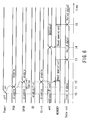
- FIG. 2 is a timing chart for various signals in the semiconductor device shown in FIG. 1, showing a state observed immediately after power-on.
- the semiconductor device 100 is powered on at a time t0 as shown in the figure. Further, as described at the beginning of this section, it is assumed that a chip enable signal and an address signal are input to the semiconductor device 100 before power-on. Then, at a time t1, when the internal power supply is completely initialized, the power-on reset signal POR is enabled. Subsequently, data should be read from the semiconductor storage device 200 according to the input address signal add.
- the transition detecting circuit does not output a transition detection signal TDS. Thus, the semiconductor storage device 200 cannot start operations. As a result, data cannot be read from the semiconductor storage device 200.
- a method of activating a semiconductor device comprises:
- a delay circuit 40 delays the power-on reset signal POR a specified time, which is provided to the logic circuit 50 through the different wire as described above.
- the "specified time” is the time required to transmit the power-on reset signal POR at least from the internal power supply 30 to the semiconductor storage device 20 and the transition detecting circuit 60.
- FIG. 4A is a circuit diagram showing an example of a configuration of the delay circuit 40. As shown in the figure, the delay circuit 40 comprises a plurality of inverters 41-1 to 41-m (m is an even number) connected together in series. The power-on reset signal POR delayed by the delay circuit is supplied to the logic circuit 50 as a delayed power-on reset signal DPOR.
- the transition detecting circuit 60 monitors the transition of the address signal add and internal chip enable signal CEint. Upon detecting a transition in at least one of these signals, the transition detecting circuit 60 outputs a transition detection signal TDS.
- the transition detection signal TDS is an operation start command intended for the semiconductor storage device 20 and supplied to the control circuit 28 of the semiconductor storage device 20.
- the semiconductor storage device 20 After receiving the power-on reset signal POR (an enabled state), the semiconductor storage device 20 starts operations upon receiving the transition detection signal TDS. That is, the semiconductor storage device 20 does not start operations before a transition occurs in either the address signal add or the internal chip enable signal CEint.
- FIG. 4B is a circuit diagram showing an example of a configuration of the transition detecting circuit 60.
- the transition'detecting circuit 60 comprises exclusive OR (XOR) gates 61-1 to 61-n (n is an integer) and 62, delay circuits 63-1 to 63-n and 64, an OR gate 65, and an AND gate 66.
- the XOR gates 61-1 to 61-n correspond to bits add(1) to add(n) of an n-bit address signal.
- the XOR gates 61-1 to 61-n perform an exclusive OR operation on the respective bits add(1) to add(n) and a signal obtained by using the delay circuits 63-1 to 63-n to delay the bits add(1) to add(n).
- the XOR gate 62 performs an exclusive OR operation on the internal chip enable signal CEint and a signal obtained by using the delay circuit 64 to delay the internal chip enable signal CEint.
- the OR gate 65 performs an OR operation on the results of the operations performed by the XOR gates 61-1 to 61-n.
- the AND gate 66 performs an AND operation on the power-on reset signal and the result of the operation performed by the OR gate 65. Of course, the power-on reset signal POR input to the AND gate 66 is not delayed by the delay circuit 40. Then, the result of the operation performed by the AND gate 66 is output as a transition detection signal TDS.
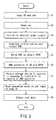
- a chip enable signal CE and an address signal add are externally input to the semiconductor device 10 (step S1).
- the address signal add indicates the address of a memory cell in which the data to be read immediately after power-on is recorded.
- the semiconductor device 10 is externally powered on (step S2).
- the internal power supply 30 is initialized (step S3).
- Initialization of the internal power supply means that the internal power supply 30 is enabled to supply a stable internal voltage on the basis of an externally provided voltage.
- the internal power supply 30 is completely initialized. Then, the internal power supply 30 enables the power-on reset signal POR (step S4).
- the power-on reset signal POR is supplied to the semiconductor storage device 20 and the transition detecting circuit 60 and is delayed by the delay circuit 40 (step S5).
- the delay circuit 40 delays the power-on reset signal POR a period Tdelay.
- the delay circuit 40 delays the power-on reset signal POR a period Tdelay.
- the delay circuit 40 delays the power-on reset signal POR a period Tdelay.
- the delay circuit 40 delays the power-on reset signal POR a period Tdelay.
- the delay circuit 40 delays the power-on reset signal POR a period Tdelay.
- the period Tdelay is required by the power-on reset signal POR to reach the semiconductor storage device 20 and the transition detecting circuit 60.
- the semiconductor storage device 20 and the transition detecting circuit 60 are returned from initialization. Returning from initialization of the semiconductor storage device 20 and the transition detecting circuit 60 means that the circuit blocks become active. Accordingly, at the time t2, when the delayed power-on reset signal DPOR is enabled, the semiconductor storage device 20 and the transition detecting circuit 60 have been returned from initialization.
- the transition detecting circuit 60 detects a transition in the internal chip enable signal CEint to output a transition detection signal TDS (step S7). That is, the transition detecting circuit 60 commands the semiconductor storage device 20 to start operations. Although already described, the transition detecting circuit 60 has already been returned from initialization and is thus active. Then, the power-on reset signal POR is enabled, and the transition detection signal TDS is output. As a result, the semiconductor storage device 20 starts operations.
- the semiconductor storage device 20 starts operations and performs a read operation on the basis of the address signal add input at step S1 (step S8). At a time t3, the semiconductor storage device outputs read data to external equipment.
- the logic circuit 50 performs an AND operation on the delayed power-on reset signal DPOR and the chip enable signal CE.
- the delay time for the power-on reset signal DPOR equals the time required by the power-on reset signal POR to reach the transition detecting circuit 60 and the semiconductor storage device 20. In other words, this is the time elapsing from power-on of the semiconductor device 10 until the transition detecting circuit 60 and the semiconductor storage device 20 are completely returned from initialization. Accordingly, when the internal chip enable signal CEint is enabled, the transition detecting circuit 60 and the semiconductor storage device 20 have already been completely returned from initialization. As a result, the transition detecting circuit 60 can accurately detect a transition in the internal chip enable signal CEint to output a transition detection signal TDS. Further, the semiconductor storage device 20 can precisely perform a read operation.
- a semiconductor device and its activation method are provided which serve to improve the reliability of a read operation performed immediately after power-on.
- the configuration according to the present embodiment allows the direct use of the conventional transition detecting circuit.
- the present embodiment can be implemented simply by adding the logic circuit 50 and the delay circuit 40 to the configuration. Therefore, the present embodiment is very simple and convenient.
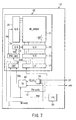
- FIG. 7 is a block diagram showing an example of a configuration of a system LSI including a semiconductor storage device.
- the LSI 10 comprises the semiconductor storage device 20, the internal power supply 30, the logic circuit 50, and the transition detecting circuit 60.
- the transition detecting circuit 60 monitors the transition of the address signal add and internal chip enable signal CEint. Upon detecting a transition in at least one of these signals, the transition detecting circuit 60 outputs a transition detection signal TDS.
- the transition detecting circuit 60 differs from the first embodiment, in that it outputs an initialization completion signal TDready to a signal line 12 when the transition detecting circuit is returned from initialization by an input power-on reset signal POR.
- FIG. 8 is a circuit diagram showing an example of a configuration of the transition detecting circuit 60 according to the present embodiment.
- the configuration of the transition detecting circuit 60 is substantially similar to that in the first embodiment, shown in FIG. 4B.
- a power-on reset signal POR provided by the internal power supply 30 is output to the signal line 12 by the transition detecting circuit 60 as an initialization completion signal TDready. That is, the initialization completion signal TDready corresponds to the power-on reset signal POR that has passed through the transition detecting circuit 60.
- the logic circuit 50 performs an AND operation on the chip enable signal CE and the initialization completion signals TDready and Mready. The result of this operation is the internal chip enable signal CEint.
- FIG. 9 is a flow chart of operations performed by the semiconductor device immediately after power-on.
- FIG. 10 is a timing chart for various signals.
- step S1 the flow from step S1 to step S4 is similar to that in the first embodiment. That is, a chip enable signal CE and an address signal add are input (step S1). Then, at the time t0, the device is powered on (step S2). Then, at the time t1, the internal power supply 30 is completely initialized (step S3). The internal power supply 30 then enables the power-on reset signal POR (step S4).
- the transition detecting circuit 60 detects a transition in the chip enable signal CEint to output a transition detection signal TDS (step S7). Then, the semiconductor storage device 20 performs a read operation on the basis of the address signal add input at step S1 (step S8). At the time t4, the semiconductor storage device 20 outputs read data to the external equipment. Description of the following operations is omitted.
- the transition detection signal TDS is enabled provided that a transition occurs in the power-on reset signal POR. Therefore, an operation of reading data from a memory cell can be performed correctly immediately after power-on.
- the transition detecting circuit 60 and the semiconductor storage device 20 outputs initialization completion signals TDready and Mready, respectively, after being returned from initialization. That is, when the internal chip enable signal CEint is enabled, the transition detecting circuit 60 and the semiconductor storage device 20 have already been returned from initialization. As a result, the transition detecting circuit 60 can accurately detect a transition in the internal chip enable signal CEint. Further, the semiconductor storage device 20 can precisely perform a read operation.
- FIG. 11C is a circuit diagram of memory cell arrays of a DRAM and a ferroelectric memory.
- a ferroelectric memory may be a series connected TC unit type ferroelectric RAM, which consists of series connected memory cells each having a transistor having a source terminal and a drain terminal and a ferroelectric capacitor arranged inbetween said two terminals, as shown in FIG. 11D.
- an MRAM Magnetic-resistive Random Access memory
- FIG. 11E can be used.
- FIG. 12 is a block diagram of a semiconductor device according to a variation of the first embodiment.
- the transition detecting circuit 60 and the semiconductor storage device 20 have been described as circuit blocks returned from initialization in response to the power-on reset signal POR. This variation indicates the case in which the device has more circuit blocks.
- the semiconductor device comprises the EEPROM 20-1, the DRAM 20-2, the SRAM 20-3, the CPU 70, the internal power supply 30, the delay circuit 40, the logic circuit 50, and the transition detecting circuit 60. It is assumed that the EEPROM 20-1, the DRAM 20-2, the SRAM 20-3, the CPU 70, and the transition detecting circuit 60 are returned from initialization upon receiving the power-on reset signal. When returned from initialization by the power-on reset signal POR, the EEPROM 20-1, the DRAM 20-2, the SRAM 20-3, the CPU 70, and the transition detecting circuit 60 output initialization completion signals Mready1, Mready2, Mready3, CPUready, and TDready.
- the logic circuit 50 performs an AND operation on the chip enable signal CE and the initialization completion signals Mready1 to Mready3, TDready, and CPUready. Then, the result of the AND operation performed by the logic circuit 50 becomes an internal chip enable signal CEint.
Applications Claiming Priority (2)
| Application Number | Priority Date | Filing Date | Title |
|---|---|---|---|
| JP2002364902A JP3990269B2 (ja) | 2002-12-17 | 2002-12-17 | 半導体装置及びその起動方法 |
| JP2002364902 | 2002-12-17 |
Publications (2)
| Publication Number | Publication Date |
|---|---|
| EP1431981A2 true EP1431981A2 (fr) | 2004-06-23 |
| EP1431981A3 EP1431981A3 (fr) | 2005-04-06 |
Family
ID=32376234
Family Applications (1)
| Application Number | Title | Priority Date | Filing Date |
|---|---|---|---|
| EP03028728A Withdrawn EP1431981A3 (fr) | 2002-12-17 | 2003-12-12 | Dispositif à semiconducteurs avec un détecteur de transition et procédé d'activation d'un tel dispositif |
Country Status (3)
| Country | Link |
|---|---|
| EP (1) | EP1431981A3 (fr) |
| JP (1) | JP3990269B2 (fr) |
| CN (1) | CN1328646C (fr) |
Families Citing this family (5)
| Publication number | Priority date | Publication date | Assignee | Title |
|---|---|---|---|---|
| US8103805B2 (en) * | 2005-04-29 | 2012-01-24 | Micron Technology, Inc. | Configuration finalization on first valid NAND command |
| KR100771140B1 (ko) | 2006-06-30 | 2007-10-29 | 엠텍비젼 주식회사 | 전원 전압 제어를 위한 동작 판별 장치 및 이를 포함하는회로 시스템 |
| JP5587156B2 (ja) * | 2010-12-13 | 2014-09-10 | ルネサスエレクトロニクス株式会社 | 不揮発性メモリを備える半導体装置及び不揮発性メモリに対するアクセス制御方法 |
| JP2012128769A (ja) * | 2010-12-17 | 2012-07-05 | Toshiba Corp | メモリシステム |
| CN106680752B (zh) * | 2012-12-18 | 2019-07-19 | 上海联影医疗科技有限公司 | 线圈测试装置、磁共振系统及其输出校正方法和装置 |
Citations (2)
| Publication number | Priority date | Publication date | Assignee | Title |
|---|---|---|---|---|
| EP0887801A2 (fr) * | 1997-06-27 | 1998-12-30 | Siemens Aktiengesellschaft | Appareil pour commander le réaction d'un circuit pendant la mise sous tension |
| US6201751B1 (en) * | 1999-03-08 | 2001-03-13 | Micron Technology, Inc. | Integrated circuit power-up controllers, integrated circuit power-up circuits, and integrated circuit power-up methods |
Family Cites Families (4)
| Publication number | Priority date | Publication date | Assignee | Title |
|---|---|---|---|---|
| KR970003810B1 (ko) * | 1993-04-14 | 1997-03-22 | 삼성전자 주식회사 | 어드레스 천이 검출회로를 내장하는 불휘발성 반도체 집적회로 |
| JPH0863264A (ja) * | 1994-08-25 | 1996-03-08 | Fujitsu Ltd | パワーオンリセット回路 |
| JP3630877B2 (ja) * | 1996-10-07 | 2005-03-23 | 株式会社リコー | インタフェース回路 |
| JPH11136109A (ja) * | 1997-11-04 | 1999-05-21 | Denso Corp | パワーオンリセット回路 |
-
2002
- 2002-12-17 JP JP2002364902A patent/JP3990269B2/ja not_active Expired - Fee Related
-
2003
- 2003-12-12 EP EP03028728A patent/EP1431981A3/fr not_active Withdrawn
- 2003-12-17 CN CNB2003101231202A patent/CN1328646C/zh not_active Expired - Fee Related
Patent Citations (2)
| Publication number | Priority date | Publication date | Assignee | Title |
|---|---|---|---|---|
| EP0887801A2 (fr) * | 1997-06-27 | 1998-12-30 | Siemens Aktiengesellschaft | Appareil pour commander le réaction d'un circuit pendant la mise sous tension |
| US6201751B1 (en) * | 1999-03-08 | 2001-03-13 | Micron Technology, Inc. | Integrated circuit power-up controllers, integrated circuit power-up circuits, and integrated circuit power-up methods |
Also Published As
| Publication number | Publication date |
|---|---|
| JP2004199238A (ja) | 2004-07-15 |
| JP3990269B2 (ja) | 2007-10-10 |
| CN1328646C (zh) | 2007-07-25 |
| EP1431981A3 (fr) | 2005-04-06 |
| CN1534781A (zh) | 2004-10-06 |
Similar Documents
| Publication | Publication Date | Title |
|---|---|---|
| US10090038B2 (en) | Semiconductor memory device for deconcentrating refresh commands and system including the same | |
| US7466623B2 (en) | Pseudo SRAM capable of operating in continuous burst mode and method of controlling burst mode operation thereof | |
| US8743644B2 (en) | Semiconductor integrated circuit having array E-fuse and driving method thereof | |
| CN111581131B (zh) | 存储装置及包括其的数据处理系统 | |
| US7778107B2 (en) | Decoding control with address transition detection in page erase function | |
| JPH09147551A (ja) | メモリデバイス回路及びマルチバンクメモリアレイのマルチバンク列の同時アドレス方法 | |
| CN102467971A (zh) | 包括熔丝阵列的半导体器件和操作其的方法 | |
| US8437209B2 (en) | Integrated circuit | |
| US9627095B1 (en) | Memory module, memory system including the same and operation method thereof | |
| US20190121720A1 (en) | Nonvolatile memory device and operation method thereof | |
| US9483193B1 (en) | Data storage device | |
| US8127069B2 (en) | Memory device including self-ID information | |
| US20060133126A1 (en) | Semiconductor memory device capable of switching from multiplex method to non-multiplex method | |
| US9251917B2 (en) | Memory device and defective address repair methods thereof | |
| US6868020B2 (en) | Synchronous semiconductor memory device having a desired-speed test mode | |
| US6636443B2 (en) | Semiconductor memory device having row buffers | |
| KR20210069514A (ko) | 메모리 시스템 및 메모리 시스템의 트레이닝 방법 | |
| US7127598B2 (en) | Semiconductor device comprising transition detecting circuit and method of activating the same | |
| EP1431981A2 (fr) | Dispositif à semiconducteurs avec un détecteur de transition et procédé d'activation d'un tel dispositif | |
| KR100434513B1 (ko) | 클럭 인에이블 신호를 이용한 데이터 경로의 리셋 회로,리셋 방법 및 이를 구비하는 반도체 메모리 장치 | |
| CN107527649B (zh) | 具有提高的延迟的存储器器件及其操作方法 | |
| CN109119122B (zh) | 地址控制电路及半导体装置 | |
| US6765831B2 (en) | Semiconductor integrated circuit device | |
| US7900099B2 (en) | Enabling test modes of individual integrated circuit devices out of a plurality of integrated circuit devices | |
| US20210391015A1 (en) | Non-volatile memory device including high voltage switching circuit, and operation method of the non-volatile memory device |
Legal Events
| Date | Code | Title | Description |
|---|---|---|---|
| PUAI | Public reference made under article 153(3) epc to a published international application that has entered the european phase |
Free format text: ORIGINAL CODE: 0009012 |
|
| 17P | Request for examination filed |
Effective date: 20031212 |
|
| AK | Designated contracting states |
Kind code of ref document: A2 Designated state(s): AT BE BG CH CY CZ DE DK EE ES FI FR GB GR HU IE IT LI LU MC NL PT RO SE SI SK TR |
|
| AX | Request for extension of the european patent |
Extension state: AL LT LV MK |
|
| PUAL | Search report despatched |
Free format text: ORIGINAL CODE: 0009013 |
|
| AK | Designated contracting states |
Kind code of ref document: A3 Designated state(s): AT BE BG CH CY CZ DE DK EE ES FI FR GB GR HU IE IT LI LU MC NL PT RO SE SI SK TR |
|
| AX | Request for extension of the european patent |
Extension state: AL LT LV MK |
|
| RIC1 | Information provided on ipc code assigned before grant |
Ipc: 7G 11C 11/4072 B Ipc: 7G 11C 5/14 B Ipc: 7G 11C 7/20 A |
|
| AKX | Designation fees paid |
Designated state(s): DE |
|
| 17Q | First examination report despatched |
Effective date: 20071129 |
|
| RAP1 | Party data changed (applicant data changed or rights of an application transferred) |
Owner name: INFINEON TECHNOLOGIES AG Owner name: KABUSHIKI KAISHA TOSHIBA |
|
| STAA | Information on the status of an ep patent application or granted ep patent |
Free format text: STATUS: THE APPLICATION IS DEEMED TO BE WITHDRAWN |
|
| 18D | Application deemed to be withdrawn |
Effective date: 20100701 |