EP1430833A1 - Fingerabdrucksensor - Google Patents
Fingerabdrucksensor Download PDFInfo
- Publication number
- EP1430833A1 EP1430833A1 EP02767950A EP02767950A EP1430833A1 EP 1430833 A1 EP1430833 A1 EP 1430833A1 EP 02767950 A EP02767950 A EP 02767950A EP 02767950 A EP02767950 A EP 02767950A EP 1430833 A1 EP1430833 A1 EP 1430833A1
- Authority
- EP
- European Patent Office
- Prior art keywords
- fingerprints
- detection
- detection electrodes
- protection film
- refractory metal
- Prior art date
- Legal status (The legal status is an assumption and is not a legal conclusion. Google has not performed a legal analysis and makes no representation as to the accuracy of the status listed.)
- Withdrawn
Links
Images

Classifications
-
- A—HUMAN NECESSITIES
- A61—MEDICAL OR VETERINARY SCIENCE; HYGIENE
- A61B—DIAGNOSIS; SURGERY; IDENTIFICATION
- A61B5/00—Measuring for diagnostic purposes; Identification of persons
- A61B5/117—Identification of persons
-
- G—PHYSICS
- G06—COMPUTING OR CALCULATING; COUNTING
- G06V—IMAGE OR VIDEO RECOGNITION OR UNDERSTANDING
- G06V40/00—Recognition of biometric, human-related or animal-related patterns in image or video data
- G06V40/10—Human or animal bodies, e.g. vehicle occupants or pedestrians; Body parts, e.g. hands
- G06V40/12—Fingerprints or palmprints
- G06V40/13—Sensors therefor
- G06V40/1306—Sensors therefor non-optical, e.g. ultrasonic or capacitive sensing
Definitions
- the present invention relates to a fingerprints detection apparatus by a capacitance detection method, particularly to detection electrodes and the wiring in a sensor portion of the apparatus.
- a fingerprints detection apparatus by a capacitance detection method as shown in FIG.7 is known (see, for example, Gazette of US Patent NO.5325442).
- the fingerprints detection apparatus includes a sensor portion, what is called a fingerprints sensor chip 2 in which a plurality of detection electrodes 4 are arranged like an array on the surface of a semiconductor substrate 3 through an insulation film 5, and an insulating protection film (surface protection film) 6 is formed so as to cover those detection electrodes 4.
- the capacitance C s formed between the detection electrodes 4 and the surface of finger 1 becomes larger in its value at a protuberance of the fingerprints because of a shorter distance between the protuberance and detection electrodes 4, whereas it becomes smaller in its value at a recess of the fingerprints because of a longer distance between the recess and detection electrodes 4. Therefore, by detecting the capacitance C s , the fingerprints detection apparatus can lift the fingerprints pattern 7.
- the surface of the fingerprints sensor chip 2 described above is exposed because of its structure in which the surface of the chip is touched by a finger. Accordingly, a ball-point pen, a coin and the like may bump against the chip surface. For this reason, the protection film 6 needs to have a sufficient mechanical strength. Besides, the protection film 6 is required to have a high dielectric constant and also have a stopping performance against mobile ions for preventing the invasion of those ions.
- An example of the mobile ions is Na ions contained in sweat on the surface of finger.
- the protection film of silicon nitride, polyimide and the like are generally used in the semiconductor process.
- these films are used for the protection film 6 of the fingerprints sensor chip 2 described above, a problem is raised that a crack will occur by, for example, an act of pricking the surface of the film with a pen point. If a crack occurs in the protection film 6, the mobile ions can not be prevented from invading, so that characteristics of a semiconductor device connected to each detection electrode 4, namely, a switching device (e.g. MOS transistor) formed on the semiconductor substrate 3 will change.
- a switching device e.g. MOS transistor
- wiring materials of aluminum or copper are generally used in the semiconductor process, but they are small in the Vickers hardness as compared with the protection film of silicon nitride, etc. If aluminum or copper is used in the detection electrodes, when an external stress F is applied thereto as shown in FIG.5, then the detection electrodes 4 will bend first. Depending on the bending amount of the detection electrodes 4, the protection film 6 also bends and cracks 8 will occur in the protection film 6, further in the insulation film 5 thereunder.
- a tolerance to crack of the protection film 6 depends on the Vickers hardness of detection electrodes 4 rather than on the mechanical strength of protection film 6 itself, and thus the tolerance goes smaller than the ability of protection film 6. This raises another problem.
- the same is applicable to the wiring 9 beneath the detection electrodes 4. As is shown in FIG.6, even if materials of high Vickers hardness is employed in the detection electrodes 4, when the Vickers hardness of wiring 9 is small, the wiring 9 will bend first if an external force F is applied. Depending on the bending amount of wiring 9, the detection electrodes 4 and also the protection film 6 will bend, thereby causing cracks 8 to be occurred in the protection film 6 and insulation film 5.
- the present invention provides a fingerprints detection apparatus in which the Vickers hardness of the detection electrodes in a sensor portion as well as the wiring beneath detection electrodes is increased, and the occurrence of cracks in a protection film and the like is restrained.
- the fingerprints detection apparatus has the structure of capacitance detection type, including the sensor portion which has an insulation film formed so as to cover a plurality of detection electrodes arranged like an array, the detection electrodes being formed of a refractory metal or a compound of refractory metal. More preferably, the detection electrodes as well as the wiring beneath the detection electrodes are formed of a refractory metal or a compound of refractory metal.
- the refractory metal includes Ti, Ta, W, and Mo, any one of which can be employed as such.
- the compound of refractory metal includes compounds of Ti, Ta, W, and Mo, any one of which can be employed as such.
- the detection electrodes or the detection electrodes as well as the wiring just thereunder in the sensor portion are formed of a refractory metal or a compound of refractory metal, the Vickers hardness of detection electrodes and wiring increases. For this reason, the mechanical strength of insulating protection film improves and the occurrence of cracks in insulating protection film is restrained even if a stress is applied from the outside.
- the fingerprints detection apparatus of the present invention by forming the detection electrodes, more preferably the detection electrodes and wiring just thereunder, of a refractory metal with high Vickers hardness or a compound of the refractory metal, particularly any one of Ti, Ta, W, and Mo, or any one of compounds of Ti, Ta, W, and Mo, a tolerance to cracks of the insulating protection film can be improved. Therefore, it is possible to provide a highly reliable fingerprints detection apparatus capable of restraining the occurrence of cracks in insulation film due to, for example, an inadvertent external stress and preventing the change of characteristics of the cell selection switching element.
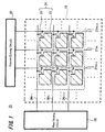
- FIG.1 shows a whole schematic structure of a fingerprints detection apparatus by the capacitance detection method according to the present invention.
- the fingerprints detection apparatus 21 includes a sensor portion ( a so-called fingerprints sensor chip ) 25 in which unitary cells 24 are arranged like an array, which cell 24 is made up of a detection electrode 22 and a cell selection switching device (e.g. a MOS transistor) 23 connected to the detection electrode 22.
- a cell selection switching device e.g. a MOS transistor
- a gate of each cell selection switching device 23 is connected to the respective row selecting lines 26 [ 26 n-1 , 26 n , 26 n+1 ..].
- a drain of each cell selection switching device 23 is connected to the respective column sensing lines 27 [ 27 m-1 , 27 m+1 ..].
- a source of each cell selection switching device 23 is connected to each detection electrode 22.
- Each one end of the row selecting lines 26 [26 n-1 , 26 n , 26 n+1 ..] is connected to a row driving circuit 28.
- Each one end of the column sensing lines 27 [ 27 m-1 , 27 m , 27 m+1 ..] is connected to a column driving circuit 29 through capacitance detecting means(not shown) including an output line, etc. depending on the kind of capacitance detection method (a current charge method, a voltage charge method).
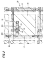
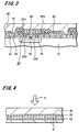
- FIG. 2 and FIG. 3 are a plan and a vertical section for showing the structure of the unitary cell 24 made up of the detection electrode 22 and cell selection switching device 23, respectively.
- the unitary cell 24 is formed on a semiconductor substrate 31 of a first conductivity type constituting the sensor portion 25.
- a semiconductor well area 32 of a second conductivity type In this semiconductor well area 32 are formed a source area 33S and a drain area 33D of the first conductivity type.
- a gate electrode 35 made of, e.g. polycrystalline silicon through a gate insulation film 34.
- a source electrode 36S and a drain electrode 36D respectively connected to the source area 33S and drain area 36D are formed, thus making a MOS transistor (e.g. n-channel MOS transistor)23 to be formed, which serves as the cell selection switching device.
- MOS transistor e.g. n-channel MOS transistor
- the drain electrode 33D of the MOS transistor 23 is formed integrated with the column sensing lines 27. Additionally, a part of the column sensing lines 27 is formed of polycrystalline silicon 38 in this example. Insulation films41 serving as interlayer films are formed so as to cover the MOS transistor 23. On the insulation film 41 is formed the detection electrode 22 connected to the source electrode 36S through a contact hole. Further, an insulating protection film 42 is formed over all surface of the sensor portion 25 so as to cover the detection electrodes 22. The insulating protection film 42 is formed of silicon nitride, silicon oxide and so on. In this example, it is formed of a silicon nitride film. In this way, the unitary cell 24 is constructed.
- the detection electrodes 22 are formed of a refractory metal with large Vickers hardness, or a compound of the refractory metal. More preferably, the detection electrodes 22 and the wiring just thereunder, namely, the wiring including the row selecting lines 26, the column sensing lines 27 (in this example, polycrystalline silicon portions 38 are excluded.), source electrodes 36S and drain electrodes 36D are formed of the refractory metal with large Vickers hardness, or the compound of the refractory metal.
- Ti, Ta, W, Mo may be employed as the refractory metal.
- Vickers hardness that of Ti is 260kg/mm 2 ; That of W is 430kg/mm 2 ; That of Mo is 290kg/mm 2 .
- Al 35kg/mm 2
- Co 85kg/mm 2 .
- Any one of compounds of Ti, Ta, W, Mo may be employed as the compound of refractory metal.
- TiC, TiN, WC, W 2 C, MoC, Mo 2 C and the like can be employed.
- the most preferable material is W. The reason is that it has the highest melting point, low resistance and the largest hardness.
- the fingerprints detection apparatus 21 operates as follows.
- the row driving circuit 28 gives row driving signals in order of the row selecting lines 26 [ 26 n-1 , 26 n , 26 n+1 ..] by scanning in a column direction, thus causing the cell selection switching devices 23 in each row to be on from row to row and the relevant detection electrodes 22 to be selected. This makes the electric charges accumulated in each detection electrode 22 of selected rows to be supplied to the capacitance detecting means through each cell selection switching device 23 and the column sensing lines 27 [ 27 m-1 , 27 m , 27 m+1 ..].
- the column driving circuit 29 outputs column driving signals sequentially by scanning in a row direction, and electric voltage into which the electric charge of detection electrodes 22 is inverted is outputted sequentially from the capacitance detecting means through the output line. This makes it possible to detect the fingerprints pattern.
- the detection electrodes 22 of its sensor portion 25 more preferably the detection electrodes 22 and the wiring 43 thereunder (row selecting lines 26, column sensing lines 27, electrodes 36S, 36D and the like: see FIG.4) of the refractory metal of Ti, Ta, W, Mo or compounds of those metals, the Vickers hardness of the detection electrodes 22 and the wiring beneath the detection electrodes 22 is made larger. Therefore, even if a stress F is applied to the surface of sensor portion 25, i.e. insulating protection film 42 from the outside, the bending amount of the detection electrodes 22 and the wiring thereunder greatly decreases and in turn the bending amount of the insulating protection film 42 is greatly reduced.
- a tolerance to cracks of the insulating protection film 42 can be improved by reducing the bending amount of insulating protection film 42.
- cracks will be hard to occur in the insulating protection film 42, further in the interlayer insulation film 41 against the external stress F. Therefore, it is possible to provide a highly reliable fingerprints detection apparatus 21 capable of restraining the occurrence of cracks due to, for example, an inadvertent external stress and preventing the change of the characteristic of cell selection switching device 23.
Landscapes
- Engineering & Computer Science (AREA)
- Physics & Mathematics (AREA)
- Health & Medical Sciences (AREA)
- Life Sciences & Earth Sciences (AREA)
- Human Computer Interaction (AREA)
- General Physics & Mathematics (AREA)
- Multimedia (AREA)
- Theoretical Computer Science (AREA)
- Biomedical Technology (AREA)
- Animal Behavior & Ethology (AREA)
- Biophysics (AREA)
- Heart & Thoracic Surgery (AREA)
- Medical Informatics (AREA)
- Molecular Biology (AREA)
- Surgery (AREA)
- Pathology (AREA)
- General Health & Medical Sciences (AREA)
- Public Health (AREA)
- Veterinary Medicine (AREA)
- Measurement Of Length, Angles, Or The Like Using Electric Or Magnetic Means (AREA)
- Image Input (AREA)
- Measurement Of The Respiration, Hearing Ability, Form, And Blood Characteristics Of Living Organisms (AREA)
- Internal Circuitry In Semiconductor Integrated Circuit Devices (AREA)
Applications Claiming Priority (3)
| Application Number | Priority Date | Filing Date | Title |
|---|---|---|---|
| JP2001294253 | 2001-09-26 | ||
| JP2001294253A JP2003093370A (ja) | 2001-09-26 | 2001-09-26 | 指紋検出装置 |
| PCT/JP2002/009283 WO2003028553A1 (fr) | 2001-09-26 | 2002-09-11 | Detecteur d'empreinte |
Publications (1)
| Publication Number | Publication Date |
|---|---|
| EP1430833A1 true EP1430833A1 (de) | 2004-06-23 |
Family
ID=19115894
Family Applications (1)
| Application Number | Title | Priority Date | Filing Date |
|---|---|---|---|
| EP02767950A Withdrawn EP1430833A1 (de) | 2001-09-26 | 2002-09-11 | Fingerabdrucksensor |
Country Status (7)
| Country | Link |
|---|---|
| US (1) | US7250774B2 (de) |
| EP (1) | EP1430833A1 (de) |
| JP (1) | JP2003093370A (de) |
| KR (1) | KR20040040398A (de) |
| CN (2) | CN101482918B (de) |
| TW (1) | TWI259407B (de) |
| WO (1) | WO2003028553A1 (de) |
Families Citing this family (17)
| Publication number | Priority date | Publication date | Assignee | Title |
|---|---|---|---|---|
| JP2004301554A (ja) * | 2003-03-28 | 2004-10-28 | Canon Inc | 電位測定装置及び画像形成装置 |
| JP4036798B2 (ja) * | 2003-07-29 | 2008-01-23 | アルプス電気株式会社 | 容量検出回路および検出方法並びに指紋センサ |
| US7075316B2 (en) * | 2003-10-02 | 2006-07-11 | Alps Electric Co., Ltd. | Capacitance detector circuit, capacitance detection method, and fingerprint sensor using the same |
| JP4447952B2 (ja) * | 2004-04-07 | 2010-04-07 | アルプス電気株式会社 | 電荷検出回路及びそれを用いた指紋センサ |
| WO2006009110A1 (ja) * | 2004-07-23 | 2006-01-26 | Nippon Telegraph And Telephone Corporation | 表面形状認識センサ装置 |
| JP4441927B2 (ja) * | 2004-10-12 | 2010-03-31 | セイコーエプソン株式会社 | 静電容量検出装置 |
| US8253696B2 (en) * | 2006-10-23 | 2012-08-28 | Patrick R. Antaki | Flexible fingerprint sensor |
| TWI341020B (en) * | 2007-08-10 | 2011-04-21 | Egis Technology Inc | Fingerprint sensing chip having a flexible circuit board serving as a signal transmission structure and method of manufacturing the same |
| FR2948602B1 (fr) * | 2009-07-30 | 2011-08-26 | Markem Imaje | Dispositif de detection de directivite de trajectoires de gouttes issues de jet de liquide, capteur electrostatique, tete d'impression et imprimante a jet d'encre continu devie associes |
| FR2971451B1 (fr) | 2011-02-11 | 2013-03-15 | Markem Imaje | Detection de plage de stimulation dans une imprimante a jet d'encre continu |
| TWI464788B (zh) * | 2011-12-22 | 2014-12-11 | Ind Tech Res Inst | 感測元件陣列及其製作方法 |
| US10203816B2 (en) * | 2013-05-07 | 2019-02-12 | Egis Technology Inc. | Apparatus and method for TFT fingerprint sensor |
| SE1351489A1 (sv) * | 2013-12-12 | 2015-06-13 | Fingerprint Cards Ab | Fingeravtrycksavkänningssystem och -metod |
| CN104051367A (zh) * | 2014-07-01 | 2014-09-17 | 苏州晶方半导体科技股份有限公司 | 指纹识别芯片封装结构和封装方法 |
| TWM493712U (zh) * | 2014-08-01 | 2015-01-11 | Superc Touch Corp | 具有遮罩功能的感應電極之生物辨識裝置 |
| TWI596716B (zh) | 2016-06-27 | 2017-08-21 | 速博思股份有限公司 | 指紋辨識裝置 |
| KR101894029B1 (ko) * | 2017-07-21 | 2018-10-04 | 울산과학기술원 | 지문 압력 듀얼 센서 및 그 제조 방법 |
Family Cites Families (16)
| Publication number | Priority date | Publication date | Assignee | Title |
|---|---|---|---|---|
| FR2568593B1 (fr) * | 1984-08-06 | 1986-09-05 | Arnaud Davitaya Francois | Procede et dispositif de croissance de couches de siliciures de metaux refractaires et couches obtenues par ce procede |
| GB2244164A (en) * | 1990-05-18 | 1991-11-20 | Philips Electronic Associated | Fingerprint sensing |
| JP3443219B2 (ja) * | 1995-11-14 | 2003-09-02 | 株式会社日立製作所 | 半導体集積回路装置およびその製造方法 |
| US5956415A (en) * | 1996-01-26 | 1999-09-21 | Harris Corporation | Enhanced security fingerprint sensor package and related methods |
| AU8379398A (en) * | 1997-06-30 | 1999-01-19 | Wisconsin Alumni Research Foundation | Nanocrystal dispersed amorphous alloys and method of preparation thereof |
| AU747878B2 (en) * | 1998-04-09 | 2002-05-30 | California Institute Of Technology | Electronic techniques for analyte detection |
| JP2000260863A (ja) * | 1999-03-10 | 2000-09-22 | Toshiba Corp | 半導体装置及びその製造方法 |
| JP3371095B2 (ja) * | 1999-03-16 | 2003-01-27 | 日本電信電話株式会社 | 表面形状認識用センサ |
| JP2001120519A (ja) * | 1999-10-22 | 2001-05-08 | Sony Corp | 指紋認識用半導体装置およびその製造方法 |
| JP2001133213A (ja) | 1999-11-08 | 2001-05-18 | Sony Corp | 半導体装置およびその製造方法 |
| KR100503581B1 (ko) * | 2001-05-18 | 2005-07-25 | 산요덴키가부시키가이샤 | 박막 트랜지스터 및 액티브 매트릭스형 표시 장치 및이들의 제조 방법 |
| US6693441B2 (en) * | 2001-11-30 | 2004-02-17 | Stmicroelectronics, Inc. | Capacitive fingerprint sensor with protective coating containing a conductive suspension |
| US7348236B2 (en) * | 2004-06-28 | 2008-03-25 | Micron Technology, Inc. | Formation of memory cells and select gates of NAND memory arrays |
| JP2006138675A (ja) * | 2004-11-10 | 2006-06-01 | Seiko Epson Corp | 静電容量検出装置 |
| JP4481806B2 (ja) * | 2004-12-03 | 2010-06-16 | アルプス電気株式会社 | 容量検出型センサ |
| KR101133758B1 (ko) * | 2005-01-19 | 2012-04-09 | 삼성전자주식회사 | 센서 및 이를 구비한 박막 트랜지스터 표시판 |
-
2001
- 2001-09-26 JP JP2001294253A patent/JP2003093370A/ja active Pending
-
2002
- 2002-09-11 CN CN200810165685XA patent/CN101482918B/zh not_active Expired - Fee Related
- 2002-09-11 EP EP02767950A patent/EP1430833A1/de not_active Withdrawn
- 2002-09-11 US US10/450,146 patent/US7250774B2/en not_active Expired - Fee Related
- 2002-09-11 CN CNA028034635A patent/CN1484512A/zh active Pending
- 2002-09-11 KR KR10-2003-7006989A patent/KR20040040398A/ko not_active Withdrawn
- 2002-09-11 WO PCT/JP2002/009283 patent/WO2003028553A1/ja not_active Ceased
- 2002-09-23 TW TW091121743A patent/TWI259407B/zh not_active IP Right Cessation
Non-Patent Citations (1)
| Title |
|---|
| See references of WO03028553A1 * |
Also Published As
| Publication number | Publication date |
|---|---|
| WO2003028553A1 (fr) | 2003-04-10 |
| CN101482918A (zh) | 2009-07-15 |
| US7250774B2 (en) | 2007-07-31 |
| TWI259407B (en) | 2006-08-01 |
| KR20040040398A (ko) | 2004-05-12 |
| US20040051155A1 (en) | 2004-03-18 |
| JP2003093370A (ja) | 2003-04-02 |
| CN101482918B (zh) | 2011-10-19 |
| CN1484512A (zh) | 2004-03-24 |
Similar Documents
| Publication | Publication Date | Title |
|---|---|---|
| EP1430833A1 (de) | Fingerabdrucksensor | |
| JP3858728B2 (ja) | 静電容量検出装置 | |
| US6399994B2 (en) | Semiconductor device for surface-shape recognition | |
| EP1138044B1 (de) | Kapazitive Sensormatrix | |
| US7205778B2 (en) | Electrostatic capacitance detecting device | |
| JP4441927B2 (ja) | 静電容量検出装置 | |
| US20060119369A1 (en) | Capacity detecting sensor | |
| KR100758516B1 (ko) | 지문 인식용 반도체 장치 | |
| KR100371115B1 (ko) | 요철 검출 센서, 지문 조합 장치 및 개인 판별 장치 | |
| US7759628B2 (en) | Detection device and electronic apparatus having plural scanning lines, detection lines, power supply lines and plural unit circuits arranged on a substrate | |
| CN107527032B (zh) | 光感测单元及光学感测阵列结构 | |
| CN1266494A (zh) | 测定极小电容的方法以及用此方法设计的传感器 | |
| KR101728627B1 (ko) | 터치 센서 | |
| EP3651208B1 (de) | Spannungssensor zur messung von mechanischer spannung in einer geschichteten metallisierungsstruktur einer mikroelektronischen komponente | |
| JP2001120519A (ja) | 指紋認識用半導体装置およびその製造方法 | |
| JP4517599B2 (ja) | 静電容量検出装置 | |
| KR20020016671A (ko) | 지문 센서 | |
| WO2004070843A1 (en) | Thin film type image sensor of high aperture ratio and a method for manufacturing thereof |
Legal Events
| Date | Code | Title | Description |
|---|---|---|---|
| PUAI | Public reference made under article 153(3) epc to a published international application that has entered the european phase |
Free format text: ORIGINAL CODE: 0009012 |
|
| 17P | Request for examination filed |
Effective date: 20030612 |
|
| AK | Designated contracting states |
Kind code of ref document: A1 Designated state(s): AT BE BG CH CY CZ DE DK EE ES FI FR GB GR IE IT LI LU MC NL PT SE SK TR |
|
| STAA | Information on the status of an ep patent application or granted ep patent |
Free format text: STATUS: THE APPLICATION HAS BEEN WITHDRAWN |
|
| 18W | Application withdrawn |
Effective date: 20050921 |