EP1428079B1 - Schaltung zur messung der ankunftszeit eines asynchronen signals - Google Patents
Schaltung zur messung der ankunftszeit eines asynchronen signals Download PDFInfo
- Publication number
- EP1428079B1 EP1428079B1 EP02757437A EP02757437A EP1428079B1 EP 1428079 B1 EP1428079 B1 EP 1428079B1 EP 02757437 A EP02757437 A EP 02757437A EP 02757437 A EP02757437 A EP 02757437A EP 1428079 B1 EP1428079 B1 EP 1428079B1
- Authority
- EP
- European Patent Office
- Prior art keywords
- circuit
- event
- register
- counter
- flip
- Prior art date
- Legal status (The legal status is an assumption and is not a legal conclusion. Google has not performed a legal analysis and makes no representation as to the accuracy of the status listed.)
- Expired - Lifetime
Links
- 230000004044 response Effects 0.000 claims abstract description 5
- 239000003990 capacitor Substances 0.000 claims description 3
- 230000008859 change Effects 0.000 claims description 3
- 230000003111 delayed effect Effects 0.000 claims description 3
- 238000000034 method Methods 0.000 claims description 2
- 230000001360 synchronised effect Effects 0.000 claims 2
- 230000001934 delay Effects 0.000 claims 1
- 238000010586 diagram Methods 0.000 description 6
- 238000005259 measurement Methods 0.000 description 5
- 230000007704 transition Effects 0.000 description 3
- 238000001514 detection method Methods 0.000 description 2
- 230000000630 rising effect Effects 0.000 description 2
- 230000004913 activation Effects 0.000 description 1
- 230000000739 chaotic effect Effects 0.000 description 1
- 230000003750 conditioning effect Effects 0.000 description 1
- 239000006185 dispersion Substances 0.000 description 1
- 230000008569 process Effects 0.000 description 1
Images
Classifications
-
- G—PHYSICS
- G04—HOROLOGY
- G04F—TIME-INTERVAL MEASURING
- G04F10/00—Apparatus for measuring unknown time intervals by electric means
- G04F10/04—Apparatus for measuring unknown time intervals by electric means by counting pulses or half-cycles of an AC
Definitions
- the present invention relates to a digital timing circuit for measuring time of arrival of an asynchronous event.
- Certain applications require a determination of the arrival time of an asynchronous event. For example, the precise distance between a laser source and a target can be ascertained by determining the time of flight for a laser light to travel from the laser source to the target. The time when the laser light hits the target is considered as an asynchronous event.
- Other applications include locating a vessel by measuring the time of flight of an electromagnetic signal from three reference transponders to the vessel that carries a fourth transponder.
- the interval between first and second events is determined with a square wave clock source started in response to the first event.
- the source derives a square wave having a first transition when started and equally spaced succeeding transitions spaced from each other by T/2, where T is the square wave period.
- a delay network having N taps is responsive to the square wave, whereby (N+1) square waves are derived.
- the taps are spaced from each other so the clock source square wave is delayed at tap k by kT/n, where n is a predetermined integer greater than 1 and k is selectively every integer from 1 to N.
- (N+1) memory elements respectively respond to the (N+1) square waves to generate a signal indicative of which half cycle of each of the (N+1) square wave is being derived when the second event occurs.
- a timing circuit is provided according to claim 1.
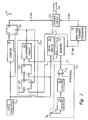
- pulse detecting circuit 17 includes an antenna 19 and a receiver 11 for receiving a signal.
- the signal can be, for example, an electromagnetic or acoustic signal.
- receiver 11 After amplifying and conditioning the signal received by antenna 19 , receiver 11 sends the received signal to a detector 12 .
- Detector 12 which is preferably formed by a series of operational amplifiers and diode detectors, then sends the received signal to a comparator 13 that includes a threshold input for eliminating spurious signals. Any signal occurs at the output of comparator 13 ( i.e., the output of pulse detecting circuit 17 ) can be treated as a trigger signal that denotes an arrival of an asynchronous event.
- the actual time of arrival of the trigger signal is measured by a counter 16 and a register 14 that is coupled to a delay circuit 15 .
- counter 16 is an m -bit counter and register 14 is a 2 n -bit register.
- a stable reference clock signal is provided to counter 16 by a clock oscillator 20 .
- Counter 16 measures the "coarse" value of the time of arrival of the trigger signal. For example, m bits of counter 16 may yield the minute or second portion for the time of arrival of the trigger signal.
- the resolution of counter 16 is dictated by the period ( i.e ., 1/frequency) of a clock signal from clock oscillator 20 .
- the number of bits within counter 16 dictates the unambiguous measurement interval for timing circuit 10 .
- the unambiguous measurement interval is the time in which a clock measurement becomes unambiguous.
- the unambiguous measurement interval for an analog clock is 12 hours, and the unambiguous measurement interval for counter 16 is preferably in the range of a few seconds.
- the bits of counter 16 are captured by a latch 24 (such as a D-type flip-flop circuit).
- the capture of m bits from counter 16 is activated by a trigger signal from the output of comparator 13 , which is the same trigger signal received by register 14 .
- the trigger signal from the output of comparator 13 activates an event circuit 29 that subsequently activates latch 24 via an enable input of latch 24 to capture m bits from counter 16 .
- the activation of latch 24 must occur synchronously with the clock cycle of a clock signal from clock oscillator 20 in order to achieve reliable operations.
- Event circuit 29 preferably includes an event flip-flop circuit 21 , a synchronizing flip-flop circuit 22 , and an adjustment circuit 23 .
- the output of event flip-flop circuit 21 is coupled to the input of synchronizing flip-flop circuit 22 that preferably changes state on a rising edge of a clock signal from clock oscillator 20 .
- the output of synchronizing flip-flop circuit 22 is coupled to a first input of adjustment circuit 23 .
- the second input of adjustment circuit 23 receives 2" output bits from register 14 .
- Register 14 is coupled to delay circuit 15 via multiple delay lines (or tap lines) 27a-27n .
- a trigger signal from the output of comparator 13
- the state of delay circuit 15 is instantaneously captured by register 14 .
- the detail of the capturing process is further explained infra.
- the 2" bits output from register 14 which are in gray code form, are sent to a gray code-to-binary converter 18 that is well-known to those skilled in the art. Gray code-to-binary converter 18 then converts the 2" gray code bits to n binary bits that represent the fraction of a clock period for the time of arrival of the trigger signal.
- the resolution of register 14 and also the resolution of gray code-to-binary converter 18 are dictated by the number of delay lines 27a-27n from delay circuit 15 .
- Delay circuit 15 is also provided with a stable reference clock signal by clock oscillator 20 .
- Delay circuit 15 which preferably includes multiple delay elements (not shown), produces a delayed fraction of a clock signal from clock oscillator 20 at the output of each delay element. For example, if delay circuit 15 has 8 delay elements, then each of the delay lines provides a delay time equal to the fraction of the period of the clock signal from clock oscillator 20 divided by 8.
- adjustment circuit 23 is to compensate for any error resulting from multiple trigger signals (i.e ., multiple asynchronous events) being captured.
- a trigger signal is captured by a D-type flip-flop circuit
- the interpretation of the resultant output from the D-type flip-flop circuit can be chaotic.
- multiple trigger signal capturings may occur in synchronizing flip-flop circuit 22 and each of the D-type flip-flop circuits within register 14 during a period of uncertainty.
- the output from register 14 is preferably taken as the correct answer, and if there is a disagreement between the information contained in the output from register 14 and the output state of synchronizing flip-flop circuit 22 .
- An Enable signal from adjustment circuit 23 is advanced or retarded as necessary to correct the output of synchronizing flip-flop circuit 22 .
- adjustment circuit 23 will logically select the last true output of register 14 , and upon a rising edge of a signal from synchronizing flip-flop circuit 22 will output an Enable signal to an enable input of latch 24 .
- the Enable signal is also used to reset event flip-flop circuit 21 via a reset input of event flip-flop circuit 21 to its quiescent state.
- the m bits from latch 24 and the n bits from gray code-to binary converter 18 are subsequently concatenated by a cascade circuit 25 to become an output having m+n bits.
- the m+n bits output is then sent to an output line 28 .
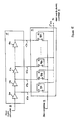
- delay circuit 15 includes delay elements 31a-31n
- register 14 includes D-type flip-flop circuits 32a-32n .
- Each of delay elements 31a-31n may be formed by two inverters connected in series, but preferably, each of delay elements 31a-31n is formed with a lumped inductor-capacitor circuit with the capacitor connected to ground.
- the output of each of delay elements 31a-31n is connected to the input (D) of each of flip-flop circuits 32a-32n via a respective one of delay lines 27a-27n .
- the outputs (Q) of flip-flop circuits 32a-32n are all coupled to gray code-to-binary converter 18 (from Figure 1 ).
- the clock inputs of flip-flop circuits 32a-32n are provided by the output of comparator 13 (from Figure 1 ).
- the total number of delay elements 31a-31n , and accordingly flip-flop circuits 32a-32n is preferably in the power of 2.
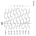
- FIG. 3 there is illustrated a timing diagram depicting the waveforms generated by various delay lines from delay circuit 15 (from Figure 2 ), in accordance with a preferred embodiment of the present invention.
- the clock signal from clock oscillator 20 is the reference clock signal for delay circuit 15 .
- delay circuit 15 has eight delay elements, and each of the eight delay elements provides a respective delay line, namely, delay lines 27a-27h .
- a trigger signal arrives at the clock input of register 14 (from Figure 2 )
- a snapshot of the state of each delay lines 27a-27h at that instant is captured by a respective flip-flop circuit within register 14 .
- a positive pulse on a delay line is captured as a logical "1," and a negative pulse on a delay line is captured as a logical "0.”
- the states of delay lines 27a-27h shown in Figure 3 are captured as "11000011.”
- the captured bits (2" bits) are preferably in gray code form. Gray code is an ordering of binary numbers such that only one bit changes from one entry to the next.
- the captured bits are not gray code bits because one bit changes from a logical "1" to a logical "0” while another bit changes from a logical "0" to a logical “1.” However, the transition from a logical "0" to a logical "1” is ignored in translating the captured bits, so the captured bits can be treated as gray code bits.
- the 2" captured bits are then converted by gray code-to-binary converter 18 (from Figure 1 ) to a binary number of n bits.
- the n bits represent the fraction of the interval between m clock periods.
- Timing circuit 10 can be implemented by sending the trigger signal to the input of delay lines 27a-27n , and capturing the state of delay element 31a-31n at the instant of a clock edge to determine the fraction of a clock period before the trigger signal.
- Event flip-flop circuit 21 , synchronizing flip-flop circuit 22 , and adjustment circuit 23 are still required for the alternative embodiment.
- the length of one complete clock signal from clock oscillator 20 is divided by the total number of delay lines within delay circuit 15 , thereby matching the delay to the period of a clock signal.
- An asynchronous event in the form of a trigger signal, triggers the capture of the elapsed time of the clock in counter 16 , and the point in the clock cycle of the receipt of the asynchronous event.
- the state of the delay lines within delay circuit 15 is captured by register 14 to provide a set of bits in gray code form.
- the gray code bits are then converted to binary bits to represent a precise fraction of one clock cycle.
- a precise time of arrival of the asynchronous event can be generated by concatenating the binary bits to the bits from counter 16 .
- the present invention provides an improved digital timing circuit for measuring time of arrival of an asynchronous event.
- the accuracy of the timing circuit of the present invention is limited only by the aperture jitter or the dispersion that can be held to fractions of a nanosecond.
Landscapes
- Engineering & Computer Science (AREA)
- Power Engineering (AREA)
- Physics & Mathematics (AREA)
- General Physics & Mathematics (AREA)
- Measurement Of Unknown Time Intervals (AREA)
- Manipulation Of Pulses (AREA)
Claims (13)
- Zeitsteuerungsschaltung (10) zum Messen der Ankunftszeit eines asynchronen Ereignisses, wobei die Zeitsteuerungsschaltung (10) Folgendes umfasst: einen Zähler (16) zum Bereitstellen einer Vielzahl von höherwertigen Binärbits als Antwort auf eine Ankunftszeit eines Triggersignals, das ein Auftreten eines asynchronen Ereignisses bezeichnet; ein Register (14) zum Bereitstellen einer Vielzahl von Gray-Codebits als Antwort auf die Ankunftszeit des Triggersignals, einen Gray-Code zu Binärcode-Umsetzer (18), der an das Register (14) gekoppelt ist zum Umsetzen der Vielzahl von Gray-Codebits in eine Vielzahl von niederwertigen Binärbits, wobei die Zeitsteuerungsschaltung (10) außerdem gekennzeichnet ist durch:eine Ereignisschaltung (29), um zwischen Ergebnissen des Zählers (16) und des Registers (14) zu entscheiden: undeine Kaskadenschaltung, die an den Gray-Code zu Binärcode-Umsetzer (18) gekoppelt ist zum Verketten der Vielzahl von höherwertigen Binärbits und niederwertigen Binärbits, um die Ankunftszeit des asynchronen Ereignisses zu formen.
- Zeitsteuerungsschaltung (10) nach Anspruch 1, außerdem einen mit dem Zähler (16) verbundenen Latch (24) umfassend, um die vom Zähler (16) empfangene Vielzahl von höherwertigen Binärbits zu latchen, und einen Taktgeber (20) mit einem Taktsignal, worin die Vielzahl von Gray-Codebits einen Ausgabezustand des Registers (14) definiert, und worin die Ereignisschaltung (29) eine Ereignis-Flipflopschaltung (21) umfasst, die für das Auftreten des Ereignistriggersignals ansprechempfindlich ist, um einen Ausgabezustand bereitzustellen, der das Auftreten des asynchronen Ereignisses anzeigt; eine mit der Ereignis-Flipflopschaltung (21) verbundene synchronisierende Flipflopschaltung (22), die für den Ausgabezustand der Ereignis-Flipflopschaltung und für das Taktsignal ansprechempfindlich ist, um einen synchronisierten Ausgabezustand bereitzustellen, der das Auftreten des asynchronen Ereignisses synchronisiert mit dem Taktsignal anzeigt, und eine Einstellschaltung (23), die mit der synchronisierenden Flipflopschaltung (22), dem Register (14) und dem Latch (24) verbunden ist und für den Ausgabezustand der synchronisierenden Flipflopschaltung (22) und den Ausgabezustand des Registers (14) ansprechempfindlich ist, um den Ausgabezustand der synchronisierenden Flipflopschaltung (22) mit dem Ausgabezustand des Registers (14) zu vergleichen, um dadurch eine Diskrepanz zwischen dem Ausgabezustand der synchronisierenden Flipflopschaltung (22) und dem Ausgabezustand des Registers (14) aufzulösen, falls die Diskrepanz auftritt.
- Zeilsteuerungsschaltung (10) nach Anspruch 1, worin die Zeitsteuerungsschaltung (10) außerdem eine Verzögerungsschaltung (15) umfasst, die für ein Referenztaktsignal ansprechempfindlich ist und eine Vielzahl von Abgriffleitungen (27a-27n) hat, um einen verzögerten Bruchteil des Referenztaktsignals bereitzustellen, wodurch ein Zustand der Verzögerungsschaltung (15) definiert wird und worin das Register (14) eine Vielzahl von Flipflopschaltungen (32a-32n) enthält, wobei jede Flipflopschaltung (32a-32n) mit einer der Abgriffleitungen (27a-27n) verbunden ist, ansprechempfindlich für das Ereignistriggersignal und zum Erfassen des Zustands der Vetzögerungsschaltung (15) positioniert.
- Zeitsteuerungsschaltung (10) nach Anspruch 3, worin die Zeitsteuerungsschaltung (10) außerdem einen Latch (24) umfasst, der mit dem Zähler (16) verbunden ist, um die vom Zähler (16) empfangene Vielzahl von höherwertigen Binärbits zu latchen (24), und einen mit dem Zähler (16) und der Verzögerungsschaltung (15) verbundenen Taktgeber (20), um dem Zähler (16) und der Verzögertungsschaltung (15) ein stabiles Taktsignal zu liefern, und worin der Latch (24) synchron mit einem Taktzyklus des Taktsignals aktiviert wird.
- Zeitsteuerungsschaltung (10) nach Anspruch 3, worin die Verzögerungsschaltung (15) eine Vielzahl von Verzögerungselementen (31a-31n) enthält und worin jedes Verzögerungselement (31a-31n) mit einer der Vielzahl von mit dem Register (14) verbundenen Abgriffleitungen (27a-27n) verbunden ist.
- Zeitsteuerungsschaltung (10) nach Anspruch 5, worin eines der Verzögerungselemente (31a-31n) eine konzentrierte Induktor-Kondensator-Schaltung enthält.
- Zeitsteuerungsschaltung (10) nach Anspruch 1, worin die Zeitsteuerungsschaltung (10) außerdem einen Latch (24) enthält, der mit dem Zähler (16) verbunden ist, um die vom Zähler (16) empfangene Vielzahl von höherwertigen Binärbits zu latchen (24), und worin die Ereignisschaltung (29) zwischen Ergebnissen des Zählers (16) und des Registers (14) durch selektives Verzögern der Aktivierung des Latches (24) der höherwertigen Binärbits entscheidet, um dadurch das Erhöhen des Zählerwerts zu ermöglichen, bevor er gelatcht wird.
- Zeitsteuerungsschaltung (10) nach Anspruch 2, worin die Unsicherheitsperiode eine Zeitperiode unmittelbar vor einer Taktflanke enthält, wenn eine von der Ausgabe des Ereignis-Flipflops (21) erhaltene Eingabe in die synchronisierende Flipflopschaltung (22) verändert werden kann, ohne eine entsprechende Verränderung im Ausgabezustand der synchronisierenden Flipflopschaltung (22) zu verursachen.
- Zeitsteuerungsschaltung (10) nach Anspruch 1, worin ein Wert der Gray-Codebits einen Bruchteil einer Taktperiode repräsentiert, die als Antwort auf die Ankunftszeit des Ereignistriggersignals abgelaufen ist.
- Zeitsteuerungsschaltung (10) nach Anspruch 1, worin die Vielzahl von höherwertigen Binärbits die Ankunftszeit des asynchronen Ereignisses repräsentiert.
- Zeitsteuerungsschaltung (10) nach Anspruch 1, worin die Vielzahl von niederwertigen Binärbits einen Bruchteil einer Taktperiode innerhalb der Ankunftszeit des asynchronen Ereignisses repräsentiert.
- Zeitsteuerungsschaltung (10) nach Anspruch 2, worin die Einstellschaltung (23) das Aktivieren des Latches (24) beschleunigt oder verzögert, wenn der Ausgabezustand des synchronisierenden Flipflops (22) mit dem Ausgabezustand des Registers (14) nicht übereinstimmt.
- Verfahren zum Messen der Ankunftszeit eines asynchronen Ereignisses unter Verwendung einer Zeitsteuerungsschaltung (10) gemäß einem vorhergehenden Anspruch.
Applications Claiming Priority (5)
| Application Number | Priority Date | Filing Date | Title |
|---|---|---|---|
| US32208501P | 2001-09-12 | 2001-09-12 | |
| US322085P | 2001-09-12 | ||
| US62938 | 2002-02-01 | ||
| US10/062,938 US6894953B2 (en) | 2001-09-12 | 2002-02-01 | Circuit for measuring time of arrival of an asynchronous event |
| PCT/US2002/027410 WO2003023524A1 (en) | 2001-09-12 | 2002-08-28 | Circuit for measuring time of arrival of an asynchronous event |
Publications (2)
| Publication Number | Publication Date |
|---|---|
| EP1428079A1 EP1428079A1 (de) | 2004-06-16 |
| EP1428079B1 true EP1428079B1 (de) | 2009-02-25 |
Family
ID=26742888
Family Applications (1)
| Application Number | Title | Priority Date | Filing Date |
|---|---|---|---|
| EP02757437A Expired - Lifetime EP1428079B1 (de) | 2001-09-12 | 2002-08-28 | Schaltung zur messung der ankunftszeit eines asynchronen signals |
Country Status (5)
| Country | Link |
|---|---|
| US (1) | US6894953B2 (de) |
| EP (1) | EP1428079B1 (de) |
| AT (1) | ATE423995T1 (de) |
| DE (1) | DE60231313D1 (de) |
| WO (1) | WO2003023524A1 (de) |
Families Citing this family (6)
| Publication number | Priority date | Publication date | Assignee | Title |
|---|---|---|---|---|
| US7043710B2 (en) * | 2003-02-13 | 2006-05-09 | Mississippi State University | Method for early evaluation in micropipeline processors |
| US8930579B2 (en) * | 2004-09-13 | 2015-01-06 | Keysight Technologies, Inc. | System and method for synchronizing operations of a plurality of devices via messages over a communication network |
| US7916048B2 (en) * | 2008-05-27 | 2011-03-29 | International Business Machines Corporation | Encoding a gray code sequence for an odd length sequence |
| CN105653238B (zh) | 2015-12-08 | 2018-10-02 | 沈阳东软医疗系统有限公司 | 一种计时方法及装置 |
| JP6386513B2 (ja) * | 2016-10-31 | 2018-09-05 | ファナック株式会社 | 測定システム |
| CN113376999B (zh) * | 2021-06-08 | 2023-01-06 | 西安电子科技大学 | 一种用于高时间分辨率时间数字转换器的特殊加法器 |
Family Cites Families (11)
| Publication number | Priority date | Publication date | Assignee | Title |
|---|---|---|---|---|
| US3631343A (en) | 1970-08-27 | 1971-12-28 | Hewlett Packard Co | Time interval averaging circuit |
| US3984815A (en) | 1975-05-02 | 1976-10-05 | Sperry Rand Corporation | Time of event recorder |
| US4651232A (en) * | 1980-02-01 | 1987-03-17 | Ampex Corporation | Method of controlling apparatus for recording and/or reproducing on a record medium |
| US4468746A (en) | 1981-12-01 | 1984-08-28 | Cincinnati Electronics Corporation | Apparatus for determining interval between two events |
| US5045854A (en) * | 1990-03-01 | 1991-09-03 | Hewlett-Packard Company | Integrated high speed synchronous counter with asynchronous read-out |
| US5199008A (en) | 1990-03-14 | 1993-03-30 | Southwest Research Institute | Device for digitally measuring intervals of time |
| US5166959A (en) * | 1991-12-19 | 1992-11-24 | Hewlett-Packard Company | Picosecond event timer |
| GB2296142B (en) | 1994-12-16 | 1998-03-18 | Plessey Semiconductors Ltd | Circuit arrangement for measuring a time interval |
| US5784599A (en) * | 1995-12-15 | 1998-07-21 | Compaq Computer Corporation | Method and apparatus for establishing host bus clock frequency and processor core clock ratios in a multi-processor computer system |
| US5703838A (en) * | 1996-02-16 | 1997-12-30 | Lecroy Corporation | Vernier delay line interpolator and coarse counter realignment |
| US5978113A (en) * | 1997-08-29 | 1999-11-02 | Kight; William Dorsey | Apparatus for remote loopback testing and isolation of loss of signal failures within synchronous optical networks |
-
2002
- 2002-02-01 US US10/062,938 patent/US6894953B2/en not_active Expired - Fee Related
- 2002-08-28 EP EP02757437A patent/EP1428079B1/de not_active Expired - Lifetime
- 2002-08-28 AT AT02757437T patent/ATE423995T1/de not_active IP Right Cessation
- 2002-08-28 WO PCT/US2002/027410 patent/WO2003023524A1/en not_active Ceased
- 2002-08-28 DE DE60231313T patent/DE60231313D1/de not_active Expired - Fee Related
Also Published As
| Publication number | Publication date |
|---|---|
| US20030048699A1 (en) | 2003-03-13 |
| US6894953B2 (en) | 2005-05-17 |
| DE60231313D1 (de) | 2009-04-09 |
| ATE423995T1 (de) | 2009-03-15 |
| WO2003023524A1 (en) | 2003-03-20 |
| EP1428079A1 (de) | 2004-06-16 |
Similar Documents
| Publication | Publication Date | Title |
|---|---|---|
| EP3647884B1 (de) | Schaltung, verfahren und zugehöriger chip zur zeitmessung, system und vorrichtung | |
| CN110887992A (zh) | 一种时钟频率检测电路 | |
| CN112968690B (zh) | 一种高精度低抖动延时脉冲发生器 | |
| JP3196254B2 (ja) | 微小時間計測方法及び微小時間計測装置 | |
| EP1428079B1 (de) | Schaltung zur messung der ankunftszeit eines asynchronen signals | |
| US6252445B1 (en) | Method and apparatus for extending a resolution of a clock | |
| JPS63190425A (ja) | カウンタ回路 | |
| EP1596219A1 (de) | Signalprozessor um eine Zeitverzögerung zu bestimmen | |
| US3473130A (en) | Pulse pair measurement | |
| EP2172787A1 (de) | Vorrichtung und Verfahren zur Erfassung eines Ziels mithilfe einer Hochgeschwindigkeits-Probennahmevorrichtung | |
| US5367543A (en) | Circuit for detecting synchronizing signal in frame synchronization data transmission | |
| GB2152778A (en) | Comparator circuit | |
| US5867125A (en) | Incremental phase and distance measurement through digital phase signature comparison | |
| US3407356A (en) | Digital synchronizer for pulses of known repetition interval but unknown phase | |
| RU2007742C1 (ru) | Устройство дискретного измерения временного интервала радиолокационной станции | |
| US4392749A (en) | Instrument for determining coincidence and elapse time between independent sources of random sequential events | |
| CN118858724B (zh) | 一种数字示波器高精度触发定位方法 | |
| US4017740A (en) | Synchronization of digital circuits by bus triggering | |
| SU262959A1 (ru) | Преобразователь временных интервалов в^цшш'-'^ | |
| RU2231228C1 (ru) | Устройство для синхронизации по циклам | |
| SU1285458A1 (ru) | Устройство дл ввода информации | |
| US5483648A (en) | Circuit for determining the arrival times of control signals supplied to microprocessors | |
| SU790218A1 (ru) | Устройство дл синхронизации сигналов тактовой последовательности | |
| SU834848A1 (ru) | Генератор серии импульсов | |
| SU961119A1 (ru) | Генератор запаздывающих и опережающих импульсов |
Legal Events
| Date | Code | Title | Description |
|---|---|---|---|
| PUAI | Public reference made under article 153(3) epc to a published international application that has entered the european phase |
Free format text: ORIGINAL CODE: 0009012 |
|
| AK | Designated contracting states |
Kind code of ref document: A1 Designated state(s): AT BE BG CH CY CZ DE DK EE ES FI FR GB GR IE IT LI LU MC NL PT SE SK TR |
|
| AX | Request for extension of the european patent |
Extension state: AL LT LV MK RO SI |
|
| 17P | Request for examination filed |
Effective date: 20040405 |
|
| 17Q | First examination report despatched |
Effective date: 20051213 |
|
| GRAP | Despatch of communication of intention to grant a patent |
Free format text: ORIGINAL CODE: EPIDOSNIGR1 |
|
| GRAS | Grant fee paid |
Free format text: ORIGINAL CODE: EPIDOSNIGR3 |
|
| GRAA | (expected) grant |
Free format text: ORIGINAL CODE: 0009210 |
|
| AK | Designated contracting states |
Kind code of ref document: B1 Designated state(s): AT BE BG CH CY CZ DE DK EE ES FI FR GB GR IE IT LI LU MC NL PT SE SK TR |
|
| REG | Reference to a national code |
Ref country code: GB Ref legal event code: FG4D |
|
| REG | Reference to a national code |
Ref country code: CH Ref legal event code: EP |
|
| REG | Reference to a national code |
Ref country code: IE Ref legal event code: FG4D |
|
| REF | Corresponds to: |
Ref document number: 60231313 Country of ref document: DE Date of ref document: 20090409 Kind code of ref document: P |
|
| PG25 | Lapsed in a contracting state [announced via postgrant information from national office to epo] |
Ref country code: FI Free format text: LAPSE BECAUSE OF FAILURE TO SUBMIT A TRANSLATION OF THE DESCRIPTION OR TO PAY THE FEE WITHIN THE PRESCRIBED TIME-LIMIT Effective date: 20090225 Ref country code: NL Free format text: LAPSE BECAUSE OF FAILURE TO SUBMIT A TRANSLATION OF THE DESCRIPTION OR TO PAY THE FEE WITHIN THE PRESCRIBED TIME-LIMIT Effective date: 20090225 |
|
| NLV1 | Nl: lapsed or annulled due to failure to fulfill the requirements of art. 29p and 29m of the patents act | ||
| PG25 | Lapsed in a contracting state [announced via postgrant information from national office to epo] |
Ref country code: SE Free format text: LAPSE BECAUSE OF FAILURE TO SUBMIT A TRANSLATION OF THE DESCRIPTION OR TO PAY THE FEE WITHIN THE PRESCRIBED TIME-LIMIT Effective date: 20090525 Ref country code: AT Free format text: LAPSE BECAUSE OF FAILURE TO SUBMIT A TRANSLATION OF THE DESCRIPTION OR TO PAY THE FEE WITHIN THE PRESCRIBED TIME-LIMIT Effective date: 20090225 |
|
| PG25 | Lapsed in a contracting state [announced via postgrant information from national office to epo] |
Ref country code: BE Free format text: LAPSE BECAUSE OF FAILURE TO SUBMIT A TRANSLATION OF THE DESCRIPTION OR TO PAY THE FEE WITHIN THE PRESCRIBED TIME-LIMIT Effective date: 20090225 |
|
| PG25 | Lapsed in a contracting state [announced via postgrant information from national office to epo] |
Ref country code: ES Free format text: LAPSE BECAUSE OF FAILURE TO SUBMIT A TRANSLATION OF THE DESCRIPTION OR TO PAY THE FEE WITHIN THE PRESCRIBED TIME-LIMIT Effective date: 20090605 Ref country code: EE Free format text: LAPSE BECAUSE OF FAILURE TO SUBMIT A TRANSLATION OF THE DESCRIPTION OR TO PAY THE FEE WITHIN THE PRESCRIBED TIME-LIMIT Effective date: 20090225 Ref country code: PT Free format text: LAPSE BECAUSE OF FAILURE TO SUBMIT A TRANSLATION OF THE DESCRIPTION OR TO PAY THE FEE WITHIN THE PRESCRIBED TIME-LIMIT Effective date: 20090812 Ref country code: DK Free format text: LAPSE BECAUSE OF FAILURE TO SUBMIT A TRANSLATION OF THE DESCRIPTION OR TO PAY THE FEE WITHIN THE PRESCRIBED TIME-LIMIT Effective date: 20090225 Ref country code: CZ Free format text: LAPSE BECAUSE OF FAILURE TO SUBMIT A TRANSLATION OF THE DESCRIPTION OR TO PAY THE FEE WITHIN THE PRESCRIBED TIME-LIMIT Effective date: 20090225 |
|
| PG25 | Lapsed in a contracting state [announced via postgrant information from national office to epo] |
Ref country code: SK Free format text: LAPSE BECAUSE OF FAILURE TO SUBMIT A TRANSLATION OF THE DESCRIPTION OR TO PAY THE FEE WITHIN THE PRESCRIBED TIME-LIMIT Effective date: 20090225 |
|
| PLBE | No opposition filed within time limit |
Free format text: ORIGINAL CODE: 0009261 |
|
| STAA | Information on the status of an ep patent application or granted ep patent |
Free format text: STATUS: NO OPPOSITION FILED WITHIN TIME LIMIT |
|
| PG25 | Lapsed in a contracting state [announced via postgrant information from national office to epo] |
Ref country code: BG Free format text: LAPSE BECAUSE OF FAILURE TO SUBMIT A TRANSLATION OF THE DESCRIPTION OR TO PAY THE FEE WITHIN THE PRESCRIBED TIME-LIMIT Effective date: 20090525 |
|
| 26N | No opposition filed |
Effective date: 20091126 |
|
| PG25 | Lapsed in a contracting state [announced via postgrant information from national office to epo] |
Ref country code: MC Free format text: LAPSE BECAUSE OF NON-PAYMENT OF DUE FEES Effective date: 20090831 |
|
| REG | Reference to a national code |
Ref country code: CH Ref legal event code: PL |
|
| GBPC | Gb: european patent ceased through non-payment of renewal fee |
Effective date: 20090828 |
|
| PG25 | Lapsed in a contracting state [announced via postgrant information from national office to epo] |
Ref country code: LI Free format text: LAPSE BECAUSE OF NON-PAYMENT OF DUE FEES Effective date: 20090831 Ref country code: CH Free format text: LAPSE BECAUSE OF NON-PAYMENT OF DUE FEES Effective date: 20090831 |
|
| REG | Reference to a national code |
Ref country code: FR Ref legal event code: ST Effective date: 20100430 |
|
| REG | Reference to a national code |
Ref country code: IE Ref legal event code: MM4A |
|
| PG25 | Lapsed in a contracting state [announced via postgrant information from national office to epo] |
Ref country code: DE Free format text: LAPSE BECAUSE OF NON-PAYMENT OF DUE FEES Effective date: 20100302 Ref country code: IE Free format text: LAPSE BECAUSE OF NON-PAYMENT OF DUE FEES Effective date: 20090828 Ref country code: FR Free format text: LAPSE BECAUSE OF NON-PAYMENT OF DUE FEES Effective date: 20090831 |
|
| PG25 | Lapsed in a contracting state [announced via postgrant information from national office to epo] |
Ref country code: GR Free format text: LAPSE BECAUSE OF FAILURE TO SUBMIT A TRANSLATION OF THE DESCRIPTION OR TO PAY THE FEE WITHIN THE PRESCRIBED TIME-LIMIT Effective date: 20090526 |
|
| PG25 | Lapsed in a contracting state [announced via postgrant information from national office to epo] |
Ref country code: GB Free format text: LAPSE BECAUSE OF NON-PAYMENT OF DUE FEES Effective date: 20090828 |
|
| PG25 | Lapsed in a contracting state [announced via postgrant information from national office to epo] |
Ref country code: IT Free format text: LAPSE BECAUSE OF NON-PAYMENT OF DUE FEES Effective date: 20090828 |
|
| PG25 | Lapsed in a contracting state [announced via postgrant information from national office to epo] |
Ref country code: LU Free format text: LAPSE BECAUSE OF NON-PAYMENT OF DUE FEES Effective date: 20090828 |
|
| PG25 | Lapsed in a contracting state [announced via postgrant information from national office to epo] |
Ref country code: TR Free format text: LAPSE BECAUSE OF FAILURE TO SUBMIT A TRANSLATION OF THE DESCRIPTION OR TO PAY THE FEE WITHIN THE PRESCRIBED TIME-LIMIT Effective date: 20090225 |
|
| PG25 | Lapsed in a contracting state [announced via postgrant information from national office to epo] |
Ref country code: CY Free format text: LAPSE BECAUSE OF FAILURE TO SUBMIT A TRANSLATION OF THE DESCRIPTION OR TO PAY THE FEE WITHIN THE PRESCRIBED TIME-LIMIT Effective date: 20090225 |