EP1426992A2 - Interrupteur électrostatique et microeléctromécanique - Google Patents
Interrupteur électrostatique et microeléctromécanique Download PDFInfo
- Publication number
- EP1426992A2 EP1426992A2 EP03104514A EP03104514A EP1426992A2 EP 1426992 A2 EP1426992 A2 EP 1426992A2 EP 03104514 A EP03104514 A EP 03104514A EP 03104514 A EP03104514 A EP 03104514A EP 1426992 A2 EP1426992 A2 EP 1426992A2
- Authority
- EP
- European Patent Office
- Prior art keywords
- contact
- substrate
- movable
- contacts
- fixed
- Prior art date
- Legal status (The legal status is an assumption and is not a legal conclusion. Google has not performed a legal analysis and makes no representation as to the accuracy of the status listed.)
- Withdrawn
Links
Images


Classifications
-
- H—ELECTRICITY
- H01—ELECTRIC ELEMENTS
- H01P—WAVEGUIDES; RESONATORS, LINES, OR OTHER DEVICES OF THE WAVEGUIDE TYPE
- H01P1/00—Auxiliary devices
- H01P1/10—Auxiliary devices for switching or interrupting
- H01P1/12—Auxiliary devices for switching or interrupting by mechanical chopper
- H01P1/127—Strip line switches
-
- H—ELECTRICITY
- H01—ELECTRIC ELEMENTS
- H01H—ELECTRIC SWITCHES; RELAYS; SELECTORS; EMERGENCY PROTECTIVE DEVICES
- H01H59/00—Electrostatic relays; Electro-adhesion relays
- H01H59/0009—Electrostatic relays; Electro-adhesion relays making use of micromechanics
-
- H—ELECTRICITY
- H01—ELECTRIC ELEMENTS
- H01H—ELECTRIC SWITCHES; RELAYS; SELECTORS; EMERGENCY PROTECTIVE DEVICES
- H01H1/00—Contacts
- H01H1/0036—Switches making use of microelectromechanical systems [MEMS]
- H01H2001/0084—Switches making use of microelectromechanical systems [MEMS] with perpendicular movement of the movable contact relative to the substrate
-
- H—ELECTRICITY
- H01—ELECTRIC ELEMENTS
- H01H—ELECTRIC SWITCHES; RELAYS; SELECTORS; EMERGENCY PROTECTIVE DEVICES
- H01H59/00—Electrostatic relays; Electro-adhesion relays
- H01H59/0009—Electrostatic relays; Electro-adhesion relays making use of micromechanics
- H01H2059/0054—Rocking contacts or actuating members
Definitions
- the present invention relates to a contact switch and an apparatus comprising the contact switch.
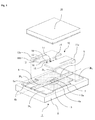
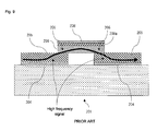
- FIG. 8 An electrostatic microrelay which is a form of the conventional contact switch is shown in Fig. 8.
- Fig. 8A a perspective view of the electrostatic microrelay is shown in Fig. 8A and its sectional view taken along line b-b is shown in Fig. 8B.
- the electrostatic microrelay mainly consists of a fixed substrate 201 comprising a glass substrate or an insulator substrate, and a movable substrate 202 comprising a semiconductor such as silicon (Si).
- a fixed electrode 204 coated with an insulating film 203, and two signal lines 205 through which a high frequency signal passes are mainly provided on the one fixed substrate 201.
- the signal lines 205 are provided so as to be spaced at a predetermined distance and ends of the signal lines provide a couple of fixed contacts 206.
- the other movable substrate 202 is fixed through an anchor 207 to be bonded to the fixed substrate 201 so as to be opposed to the fixed substrate 201.
- a movable electrode 208 positioned so as to correspond to the fixed electrode 204 is provided and a movable contact 209 which is electrically insulated from the movable electrode 208 is positioned so as to correspond to the fixed contacts 206.
- a first elastic support portion 211 constituted by a notch is formed between the anchor 207 and the movable electrode 208 to elastically support the movable electrode 208
- a second elastic support portion 212 constituted by a notch is formed between the movable electrode 208 and the movable contact 209.
- the first elastic support portion 211 and the second elastic support portion 212 are not elastically deformed and a state in which they horizontally extend from the anchors 207 is maintained while a voltage is not applied between the fixed electrode 204 and the movable electrode 208 and electrostatic attraction force is not generated.
- the electrostatic attraction force acts on the movable electrode 208
- the first elastic support portion 211 having elastic force smaller than that of the second elastic support portion 212 is elastically deformed first, and the movable electrode 208 and the movable contact 209 come close to the fixed electrode 204 and the fixed contacts 206, respectively while they keep parallel state thereof.
- the movable contact 209 comes in contact with the fixed contacts 206 and the two signal lines 205 are electrically connected.
- the movable electrode 208 is drawn by the electrostatic attraction force and sticks to the fixed electrode 204.
- the second elastic support portion 212 is elastically deformed.
- the movable contact 209 is pushed to the fixed contacts 206 by spring elasticity caused by the deformation of the second elastic support portion 212.
- the electrostatic microrelay when it is closed, the movable contact 209 and the fixed contacts 206 are closed by two-stage elastic deformation in which the first elastic support portion 211 is elastically deformed first and then, the second elastic support portion 212 is elastically deformed.
- the electrostatic attraction force disappears.
- the movable substrate 202 is separated from the fixed substrate 201 by force of restitution of the first elastic support portion 211 and the second elastic support portion 212 and returned to the original position. Accordingly, the movable contact 209 is vertically lifted by this restitution force to be separated from the fixed contacts 206 and electrical connection between the two signal lines 205 is cut off.
- a cap 210 formed of glass is bonded on the upper surface of the fixed substrate 201 through a bonding layer (not shown) in order to protect the movable substrate 202 from an outside foreign substance such as dust.
- the gap amount between the contacts is influenced by film thickness variation in the film of the fixed contacts 206 in the device manufacturing process of the contact switch, thickness variation of an insulator for insulating the movable contact 209 from the movable electrode 208 and a conductor for constituting the movable contact 209, and processing precision at the time of processing the contacts.
- the precision variation in the above described variations is largest at the portion of the fixed contacts 206 (in the circle designated by a dotted line in Fig. 8) formed by the thickest film.
- the thickness of the wiring has to be a skin depth or more in consideration of a skin effect.
- a distance between the movable electrode 208 and the fixed electrode 204 (distance between electrode gaps) when the movable contact 209 and the fixed contacts 206 are closed and come in contact with each other is smaller than the design value.
- a displacement amount of the movable electrode 208 from the state in which the contacts are closed until the state in which the fixed electrode 204 and the movable electrode 208 come in contact with each other by electrostatic attraction force becomes small
- a displacement amount of the second elastic support portion 212 which starts spring deformation from the state in which the contacts are closed becomes small also.
- force acting on the movable contact 209 from the second elastic support portion 212 is designated by the above described spring design based on the displacement amount set on the basis of the state in which the contacts are closed.
- the elastic force acting on the second movable contact 209 is decreased because the displacement amount of themovable electrode 208 is decreased. Consequently, the movable contact 209 cannot be sufficiently pushed toward the fixed contacts 206 so that contact reliability cannot be secured.
- the distance gap between the movable electrode 208 and the fixed electrode 204 when the movable contact 209 and the fixed contacts 206 are closed to be in contact with each other is more than the design value.
- electrostatic attraction force acting on the movable electrode 208 toward the fixed electrode 204 is reduced.
- the electrostatic attraction force becomes smaller than the sum of the elastic force of the first elastic support portion 211 and the second elastic support portion 212 a phenomenon in which the fixed electrode 204 and the movable electrode 208 do not contact with each other could occur.
- One or more embodiments of the present invention provide a contact switch and an apparatus provided with the contact switch, in which variation of the gap amount between contacts is reduced by reducing film thickness variation at the part of the contacts by a simple change of a structure and contact reliability between the contacts when they are closed is secured, and operations can be stabilized.
- one or more embodiments of the present invention provide a contact switch in which high frequency characteristics can be improved and loss in transmission of a high frequency signal can be reduced.
- a contact switch comprises a first contact provided on a substrate, a second contact to be closed or opened with the first contact, and a plurality of signal lines provided on the substrate, insulated with each other, and connected when the first contact and the second contact are closed, and it is characterized in that a film thickness of the first contact is smaller than that of the signal lines.
- the wiring film thickness can be set at a desired film thickness without influencing contact force, variation in film thickness at the portion of contacts having film thickness smaller than that of the signal lines can be the minimum, the variation of the gap between the contacts can be reduced, the contact reliability between the contacts when they are closed is secured, and operations can be stabilized.
- a skin depth required for flowing a current can be secured in the film thickness of the signal lines, the high frequency characteristics can be improved and the loss in transmission of the high frequency signal can be reduced.
- the contact switch comprises a first contact provided on a substrate, a second contact to be closed or opened with the first contacts, and a plurality of signal lines provided on the substrate, insulated with each other, and connected when the first contacts and the second contact are closed, and it is characterized in that the contact switch in which a film thickness of the first contacts is smaller than that of the signal lines opens and closes a signal.
- the apparatus using the contact switch comprises an apparatus such as a wireless communication equipment or a measuring equipment, which opens and closes the high frequency signal.
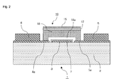
- Fig. 1 shows an exploded perspective view showing a microrelay as a contact switch according to a first embodiment of the present invention.
- Fig. 2 shows sectional views showing the microrelay as the contact switch when it is closed according to the first embodiment of the present invention.
- Fig. 3 shows sectional views showing operations of the microrelay as the contact switch according to the first embodiment of the present invention.
- Fig. 4 shows sectional views showing manufacturing processes of the microrelay as the contact switch according to the first embodiment of the present invention.
- Fig. 5 shows a sectional view and a plan view showing a contact portion of the microrelay as the contact switch when it is closed and a transmitting state of a high frequency signal according to the second embodiment of the present invention.
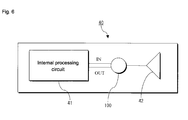
- Fig. 6 shows a bock diagram showing a wireless communication equipment as an example of an apparatus provided with the contact switch of the present invention, according to a third embodiment of the present invention.
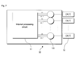
- Fig. 7 shows a bock diagram showing a measuring equipment as an example of an apparatus provided with the contact switch of the present invention, according to the third embodiment of the present invention.
- Fig. 8 shows a perspective view showing a structure of a microrelay as a contact switch and sectional views showing its operations according to the prior art.
- Fig. 9 shows a sectional view for explaining a problem referring to transmission of a high frequency signal in the contact switch according to the prior art.
- Fig. 1 shows a microrelay as the contact switch according to the first embodiment.
- the electrostatic microrelay according to the first embodiment has a constitution in which a movable substrate 10 is integrated on a surface of a fixed substrate 1 at a predetermined distance, and a cap 20 is provided so as to cover the movable substrate 10.
- At least one fixed electrode 3 and two signal lines 4 and 5 are provided on an upper surface of a glass substrate 2.
- the signal lines 4 and 5 are disposed on the same line (two-dot chain line in Fig 1).
- the fixed electrode 3 is provided in a vicinity of the signal lines 4 and 5 at a predetermined distance so as to surround them and its surface is coated by an insulating film 7.
- the fixed electrode 3 is used also as a GND electrode (earth electrode) of a high frequency signal transmitting through the signal lines 4 and 5 to constitute Coplanar structure.
- isolation characteristics can be improved.
- the isolation characteristics show how much leakage of the high frequency signal exists between the signals when the contacts are opened.
- improvement in the isolation characteristics means reduction of the leakage of the high frequency signal.
- connection pads 3b 1 and 3b 2 External ends of the signal lines 4 and 5 are electrically connected to connection pads 3b 1 and 3b 2 , and connection pads 3b 3 and 3b 4 , respectively.
- one end of the signal lines 4 and 5 in the vicinity of the center (inside a circle designated by a dotted line) of the fixed substrate 1 constitute fixed contacts 4a and 5a disposed at a predetermined distance.
- the fixed contacts 4a and 5a are formed so as to have a film thickness smaller than that of the signal lines 4 and 5. More specifically, the signal lines 4 and 5 and the fixed contacts 4a and 5a have a stepped configuration so as to form a concave portion in the center of the fixed substrate 1.
- the film thickness variation of the fixed contacts 4a and 5a can be reduced by reducing the film thickness of the fixed contacts 4a and 5a.
- an error amount is determined by a ratio to a process amount (basic dimension), when the film thickness issmall and the basic dimension becomes small, the absolute value of the error amount can be reduced and the film thickness variation can be reduced.
- a first electrically conductive layer formed in the same manufacturing process as the fixed electrode 3 is patterned so as to protrude from the signal lines 4 and 5 by the fixed contacts 4a and 5a.
- the signal lines 4 and 5 are formed by laminating a second electrically conductive layer on the first electrically conductive layer.
- the second conductive layer is formed of silver (Ag), copper (Cu), gold (Au), aluminum (Al) or the like so that the second conductive layer can be conductive with the first conductive layer and the first conductive layer is exposed only at the fixed contacts 4a and 5a at the one ends of the signal lines 4 and 5.
- the exposed portions have a configuration in which they can be closed with a movable contact 18 on the movable substrate 10 to be described later.
- the fixed contacts 4a and 5a are formed of the same electrically conductive thin film as the fixed electrode 3, and the signal lines 4 and 5 in which the second conductive layer is laminated thereon are formed so as to have a skin depth ⁇ ( ⁇ m) or more which is determined by the following equation (1) from electric conductivity ⁇ (s/m) of a conductive material (a material of the second conductive layer) mainly constituting the signal lines 4 and 5, and a frequency ⁇ (GHz) of an electric signal passing through the signal lines 4 and 5.
- ⁇ 10 5 2 ⁇ 1 ⁇ ( ⁇ m )
- the skin depths required for transmitting the predetermined frequency signal are shown in Table 1.
- Table 1 shows that the skin depth depends on the material of the signal lines and the frequency of the electric signal passing through the signal lines.
- Frequency(GHz) 0.1 0.3 0.5 1 3 5 10
- Skin Depth ( ⁇ m) Silver 6.44 3.72 2.88 2.04 1.18 0.91 0.64 Copper 6.61 3.82 2.96 2.09 1.21 0.93 0.66 Gold 7.86 4.54 3.52 2.49 1.44 1.11 0.79 Aluminum 7.96 4.59 3.56 2.52 1.45 1.13 0.80
- the film thickness of the signal lines 4 and 5 is determined so as to be the skin depth or more, which is determined depending on the wiring material mainly constituting the signal lines 4 and 5 and the frequency of the signal used in an apparatus provided with the contact switch, the high frequency signal can be transmitted with low loss. Furthermore, even when the film thickness of the fixed contacts 4a and 5a is not more than the skin depth, if the sum of the film thicknesses of the fixed contacts 4a and 5a and the movable contact 18 is the skin depth or more when they are closed with the movable contact 18 to be described later, the high frequency signal can be transmitted with low loss.
- the film thickness of the fixed contacts 4a and 5a can be set small without receiving limitation of the skin depth by forming the fixed contacts 4a and 5a of the signal lines 4 and 5 into the stepped configuration, its variation amount can be reduced as compared to the prior art.
- the multilayer constitution for securing the film thickness of the other signal lines 4 and 5, the wiring portion 6a and the connection pads 3b 1 to 3b 4 and 6b since there is no influence on the gap amount between the contacts, the degree of freedom is increased for film thickness. Therefore, when their conductive layers are formed, a general film forming method can be employed and a sufficient film thickness considering a skin effect can be obtained.
- the conductive materials shown in Table 1 have low adhesiveness with the insulating material such as the glass substrate 2 in many cases. Therefore, when the substrate formed of the insulating material such as the glass substrate 2 like in the first embodiment is used, it is preferable that the first conductive layer is an adhesive layer formed of a conductive material such as chrome (Cr), titanium (Ti), or a conductive compound and then the conductive material constituting the second conductive layer is disposed on this adhesive layer.
- a conductive material such as chrome (Cr), titanium (Ti), or a conductive compound
- a diffusion prevention layer formed of nickel (Ni), ruthenium (Ru), tungsten (W), tantalum (Ta), or the like is provided between the second conductive layer and the adhesive layer.
- the adhesive layer, or the laminated film consisting of the adhesive layer and diffusion prevention layer forms the first conductive layer, and the first conductive layer is used for the fixed electrode 3 and the fixed contacts 4a and 5a.
- the fixed electrode 3 and the fixed contacts 4a and 5a can be formed at the same manufacturing process. Therefore, after the signal lines 4 and 5 are formed, the fixed contacts 4a and 5a can be formed only by changing a mask configuration of patterning such as wiring without newly adding a process for forming the stepped configuration.
- a silicon (Si) substrate is processed to form the movable substrate 10, on which anchors 11a and 11b, a first elastic support portion 12, a movable electrode 13, a second elastic support portion 14, and the movable contact portion 15 are formed.
- the movable electrodes 13 are supported by the first elastic support portions 12 as two first beam portions which extend sideward from the anchors 11a and 11b which are to be bonded on the upper face edge of the fixed substrate 1.
- the anchors 11a and 11b are positioned so as to be almost point symmetrical about the movable contact portion 15 with each other and constituted so as to be set in two portions in the upper face of the fixed substrate 1.
- one anchor 11b is electrically connected to the connection pad 6b through the wiring portion 6a provided on an upper face of the fixed substrate 1.
- the first elastic support portions 12 are constituted by slits 12a formed into a configuration in which upper end portions of the anchors 11a and 11b are extended.
- the first elastic support portions 12 have a thickness smaller than that of the anchors 11a and 11b and spaced from the fixed substrate 1 at a predetermined distance.
- the movable electrode 13 is supported by an end portion on the opposite side of the first elastic support portion 12 to the anchors 11a and 11b, and positioned so as to be opposed to the fixed electrode 3 at a predetermined distance.
- the movable electrode 13 is constituted so as to be drawn to the side of the fixed electrode 3 by electrostatic attraction force generated when a voltage is applied between the fixed electrode 3 and the movable electrode 13.
- the second elastic support portion 14 serving as a second beam consisting of a pair of connection portions are formed in the center of the movable electrode 13.
- the movable substrate 10 is constituted such that the movable contact portion 15 is elastically supported in the center of the elastically supported movable electrode 13 through the second elastic support portion 14.
- the second elastic support portion 14 and the movable contact portion 15 are formed by a portion remained after a notched portion 16 is notched from both edges of the movable substrate 10 toward the center thereof.
- the second elastic support portion 14 is a beam having a narrow width which connects the movable electrode 13 to the movable contact portion 15, which is formed so as to be able to secure elastic force stronger than that of the first elastic support portion 12 when the contacts are closed.
- the movable contact portion 15 protrudes toward the anchors 11a and 11b so as to be thicker than the second elastic support portion 14 by a reduced film thickness of the fixed contacts 4a and 5a.
- a movable contact 18 is provided in the center of the movable contact portion 15 on the side of the fixed substrate 1 through the insulating film 17.
- the movable contact 18 is provided so as to be opposed to the fixed contacts 4a and 5a so that they can be in contact with each other or separated from each other.
- the movable contact 18 is formed to electrically connect the signal lines 4 and 5 with each other when it is closed with the isolated respective fixed contacts 4a and 5a.
- a concave portion 18a formed of a cavity in which a predetermined clearance is added to a height of the insulating film 7 is provided in a part of the movable contact 18 opposed to the fixed electrode 3 (that is, a part could be in contact with the fixed electrode 3) on the side of the fixed substrate 1.
- the double-break movable contact 18 is constituted so as to have at least two stepped heights and positioned at a space between the signal lines 4 and 5 when the movable contact 18 and the fixed contacts 4a and 5a are closed.
- the movable contact 18 and the fixed contacts 4a and 5a are closed or opened, the movable contact 18 can be prevented from coming in contact with the fixed electrode 3, and an influence such as an increase in noise in the high frequency signal can be avoided.
- At least a portion opposed to the signal lines 4 and 5 is removed by the notched portion 16 in the movable elect rode 13. Therefore, since capacity coupling is reduced between the movable electrode 13 and the signal lines 4 and 5, the isolation characteristics can be improved.
- the movable substrate 10 is sealed by the cap 20 in a state in which the movable substrate 10 is fixed to the fixed substrate 1 to constitute the microrelay according to the first embodiment.
- FIG. 3 shows operating states of the microrelay according to the first embodiment.
- the first elastic support portions 12 is not elastically deformed in a state in which a voltage is not applied between the fixed electrode 3 and the movable electrode 13 and electrostatic attraction force is not generated, and maintains a state in which they extend from the anchors 11a and 11b horizontally.
- the movable substrate 10 is opposed to the fixed substrate 1 at a predetermined distance.
- the movablecontact 18 is separated from the fixed contacts 4a and 5a.
- the first elastic support portion 12 having elastic force smaller than that of the second elastic support portion 14 is elastically deformed first as shown in Fig. 3B, and the movable electrode 13 comes close to the fixed electrode 3.
- the movable contact 18 comes in contact with the fixed contacts 4a and 5a because the movable electrode 13 around it is drawn toward the fixed electrode 3.
- the movable electrode 13 sticks to the insulating film 7 which coats the fixed electrode 3 as shown in Fig. 3C.
- the second elastic support portion 14 is elasticallydeformedandthemovable contact 18 is pressedtoward the fixed contacts 4a and 5a by the spring elasticity of the second elastic support portion 14.
- the signal is cut off in the state shown in Fig. 3A and the signal is transmitted in the states shown in Figs. 3B and 3C.
- the signal is opened and closed.
- FIG. 4 shows manufacturingprocesses of the microrelay according to the first embodiment.
- an electrically conductive layer serving as an adhesive layer and a diffusion prevention layer is formed on the glass substrate 2 shown in Fig. 4A and patterned to form a lower conductive layer (the first conductive layer) of the signal lines 4 and 5 including the fixed electrode 3 and the fixed contacts 4a and 5a as shown in Fig. 4B. Then, a print wiring, a connection pad, and an upper layer of the signal lines (the second conductive layer) are formed thereon (not shown in Fig. 4).
- the insulating film 7 is formed on the fixed electrode 3.
- the fixed substrate 1 shown in Fig. 4C is formed.
- the insulating film 7 silicon oxide (SiO 2 ) film having a dielectric constant of 3 to 4
- Great electrostatic attraction force can be obtained by using these insulating materials when the contacts and the electrodes are opened and closed, whereby the contacting force can be increased.
- an etching mask 22 formed of an SiO 2 film and having a configuration of a predetermined pattern is formed on a surface of an SOI (Silicon On Insulator) wafer on which a silicon (Si) layer 21a, a silicon oxide (SiO 2 ) layer 21b and Si layer 21c are sequentially formed from the upper side.
- SOI Silicon On Insulator
- the Si layer 21c is etched away using the etching mask 22 as amask. Then, as shown in Fig. 4E, the anchors 11a and 11b protruding downward are formed. In addition, a convex portion 21d is formed by reducing an etching amount at the portion, where the movable contact portion 15 is formed, in the Si layer 21c.
- the insulating film 17 is selectively formed at a region of the convex portion 21d on the surface of the SOI substrate 21 at a predetermined distance between the contacts.
- the movable contact 18 is formed on the insulting film 17. Since the convex portion 21d is formed at the movable contact 18, the gap amount between the contacts is the same while the film thickness of the movable contact can be equally maintained like in the prior art.
- the upper surface of the SOI substrate 21 is etched away using the SiO 2 layer 21b as an etching stop layer, by a wet etching method using alkali etching solution such as potassium hydroxide so that the film is thinned.
- the SiO 2 layer 21b is removed using fluorine etching solution and the movable substrate 10 formed of the Si layer 21c, on which the movable electrode 13 is formed is exposed as shown in Fig. 3I.
- die-cut etching is performed by a dry etching method such as a reactive ion etching (RIE) method, for example.
- RIE reactive ion etching
- dicing is performed using a laser or a cutter and a microrelay is cut out and the microrelay according to the first embodiment is provided.
- the film thickness of the portion of the fixed contacts 4a and 5a of the signal lines 4 and 5 is thinned by forming the stepped configuration, variation of the gap amount between the contacts can be reduced as compared to with the prior art. Furthermore, since the film thickness of the signal transmitting portion such as other signal lines 4 and 5, the wiring portion 6a, the connection pad 3b 1 to 3b 4 or the like can be determined regardless of the gap amount between the contacts, the degree of freedom regarding the film thickness variation can be increased and a sufficient film thickness considering a skin effect can be obtained.
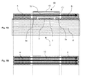
- Fig. 5 shows a sectional view of a microrelay according to the second embodiment when it is closed.
- the microrelay according to the second embodiment is constituted such that a height of an upper face of a movable contact 18 and heights of the signal lines 4 and 5 may be the same when the movable contact 18 and the fixed contacts 4a and 5a are closed.
- a width of the movable contact 18 in the direction perpendicular to the longitudinal direction of the signal lines 4 and 5 may be almost the same as that of the signal lines 4 and 5.
- mismatching can be considerably controlled as compared to the prior art.
- the second embodiment since the same effect as in the first embodiment can be provided.
- the transmission of the high frequency signal is bent at the contact portion, so that mismatching of impedance is generated and the high frequency signal is lost when the conventional contact switch is used in opening and closing the high frequency signal as shown in Fig. 9, according to the contact switch of this second embodiment, the loss of the high frequency signal when the fixed contacts 4a and 5a and the movable contact 18 are closed can be reduced even in the case of the further high frequency signal. Consequently, the mismatching of impedance at the contact portion can be further improved and the loss of the high frequency signal can be further reduced.
- Fig. 6 shows a wireless communication equipment
- Fig. 7 shows a measuring equipment.
- the microrelay according to the present invention provides characteristics capable of favorably transmitting the high frequency signal especially with low loss because of its structure characteristics.
- a microrelay 100 according to the present invention is provided so as to be connected between an internal processing circuit 41 and a two-way antenna 42 in a wireless communication equipment 40.
- the microrelay 100 according to the present invention can be used as an antenna switch which is used at a place where the high frequency signal is received from the two-way antenna 42 or the signal is supplied from the internal processing circuit 41 to the two-way antenna 42.
- the loss of the high frequency signal especially can be reduced by employing the microrelay 100 according to the present invention as the antenna switch as compared to the prior art, a load of an amplifier or the like which is used in an internal circuit can be reduced and high efficiency can be implemented because of low loss, miniaturization and low power consumption.
- a microrelay 100 is connected in the middle of the signal line extending from an internal processing circuit 51 to a measurement object 52.
- the microrelay 100 of the present invention is used as an output and supply relay between the measurement object 52 and the internal processing circuit 51 of the measuring equipment 50, the signal can be transmitted with high precision because of the characteristics of low loss transmission as compared to the switching device in the prior art.
- the first conductive layer constituting the fixed electrode 3 and the fixed contacts 4a and 5a may be formed of the conductive layer of a single layer, or the conductive layer constituting the fixed electrode 3 and the fixed contacts 4a and 5a may have a multilayer constitution in which different conductive layers are laminated.
- the signal lines 4 and 5 are not always constituted by the single material and they can be constituted by a multilayer film in which the plural kinds of materials are laminated.
- the used wiring material is not limited to the above metal material.
- the movable substrate 10 is constituted by processing the Si substrate so that the movable substrate 10 itself becomes a conductor so as to serve as the movable electrode also in the above first embodiment
- the movable electrode 13 may be constituted by providing a conductor on the base substrate.
- the present invention is not always limited to the electrostatic actuator and can be applied to a piezoelectric actuator or a thermal actuator.
Landscapes
- Contacts (AREA)
- Micromachines (AREA)
Applications Claiming Priority (2)
| Application Number | Priority Date | Filing Date | Title |
|---|---|---|---|
| JP2002354041 | 2002-12-05 | ||
| JP2002354041 | 2002-12-05 |
Publications (2)
| Publication Number | Publication Date |
|---|---|
| EP1426992A2 true EP1426992A2 (fr) | 2004-06-09 |
| EP1426992A3 EP1426992A3 (fr) | 2005-11-30 |
Family
ID=32310743
Family Applications (1)
| Application Number | Title | Priority Date | Filing Date |
|---|---|---|---|
| EP03104514A Withdrawn EP1426992A3 (fr) | 2002-12-05 | 2003-12-03 | Interrupteur électrostatique et microeléctromécanique |
Country Status (1)
| Country | Link |
|---|---|
| EP (1) | EP1426992A3 (fr) |
Cited By (6)
| Publication number | Priority date | Publication date | Assignee | Title |
|---|---|---|---|---|
| EP1703531A2 (fr) * | 2005-03-18 | 2006-09-20 | Omron Corporation | Microinterrupteur électrostatique, procédé de production correspondant et appareil comprotant le même. |
| WO2007007206A3 (fr) * | 2005-03-18 | 2007-06-14 | Simpler Networks Inc | Actionneurs et commutateurs mems |
| DE102006001321B3 (de) * | 2006-01-09 | 2007-07-26 | Protron Mikrotechnik Gmbh | Mikromechanischer Hochfrequenz-Schalter für koplanare Wellenleiter |
| DE102007035633A1 (de) | 2007-07-28 | 2009-02-19 | Protron Mikrotechnik Gmbh | Verfahren zur Herstellung mikromechanischer Strukturen sowie mikromechanische Struktur |
| EP2073237A3 (fr) * | 2007-12-20 | 2013-01-02 | General Electric Company | Microrupteur MEMS disposant d'un double actionneur et porte partagée |
| WO2015200307A3 (fr) * | 2014-06-25 | 2016-02-25 | General Electric Company | Micro-commutateurs électromécaniques intégrés et procédé associé |
Family Cites Families (3)
| Publication number | Priority date | Publication date | Assignee | Title |
|---|---|---|---|---|
| DE10080131D2 (de) * | 1999-01-25 | 2002-04-25 | Gfd Ges Fuer Diamantprodukte M | Mikroschaltkontakt |
| US6496351B2 (en) * | 1999-12-15 | 2002-12-17 | Jds Uniphase Inc. | MEMS device members having portions that contact a substrate and associated methods of operating |
| WO2001082323A1 (fr) * | 2000-04-21 | 2001-11-01 | Omron Corporation | Relais statique et dispositif de communication utilisant ledit relais statique |
-
2003
- 2003-12-03 EP EP03104514A patent/EP1426992A3/fr not_active Withdrawn
Non-Patent Citations (1)
| Title |
|---|
| None |
Cited By (11)
| Publication number | Priority date | Publication date | Assignee | Title |
|---|---|---|---|---|
| EP1703531A2 (fr) * | 2005-03-18 | 2006-09-20 | Omron Corporation | Microinterrupteur électrostatique, procédé de production correspondant et appareil comprotant le même. |
| WO2007007206A3 (fr) * | 2005-03-18 | 2007-06-14 | Simpler Networks Inc | Actionneurs et commutateurs mems |
| EP1703531A3 (fr) * | 2005-03-18 | 2007-08-15 | Omron Corporation | Microinterrupteur électrostatique, procédé de production correspondant et appareil comprotant le même. |
| CN100459010C (zh) * | 2005-03-18 | 2009-02-04 | 欧姆龙株式会社 | 静电微开关及其制造方法、以及具有静电微开关的装置 |
| US7719066B2 (en) | 2005-03-18 | 2010-05-18 | Omron Corporation | Electrostatic micro switch, production method thereof, and apparatus provided with electrostatic micro switch |
| US8115576B2 (en) | 2005-03-18 | 2012-02-14 | Réseaux MEMS, Société en commandite | MEMS actuators and switches |
| DE102006001321B3 (de) * | 2006-01-09 | 2007-07-26 | Protron Mikrotechnik Gmbh | Mikromechanischer Hochfrequenz-Schalter für koplanare Wellenleiter |
| DE102007035633A1 (de) | 2007-07-28 | 2009-02-19 | Protron Mikrotechnik Gmbh | Verfahren zur Herstellung mikromechanischer Strukturen sowie mikromechanische Struktur |
| DE102007035633B4 (de) * | 2007-07-28 | 2012-10-04 | Protron Mikrotechnik Gmbh | Verfahren zur Herstellung mikromechanischer Strukturen sowie mikromechanische Struktur |
| EP2073237A3 (fr) * | 2007-12-20 | 2013-01-02 | General Electric Company | Microrupteur MEMS disposant d'un double actionneur et porte partagée |
| WO2015200307A3 (fr) * | 2014-06-25 | 2016-02-25 | General Electric Company | Micro-commutateurs électromécaniques intégrés et procédé associé |
Also Published As
| Publication number | Publication date |
|---|---|
| EP1426992A3 (fr) | 2005-11-30 |
Similar Documents
| Publication | Publication Date | Title |
|---|---|---|
| US6753487B2 (en) | Static relay and communication device using static relay | |
| US4855544A (en) | Multiple level miniature electromechanical accelerometer switch | |
| US7489228B2 (en) | Low power consumption bistable microswitch | |
| US8018308B2 (en) | Downward type MEMS switch and method for fabricating the same | |
| US4742263A (en) | Piezoelectric switch | |
| CA1269129A (fr) | Commutateur piezoelectrique | |
| JP4447940B2 (ja) | マイクロスイッチング素子製造方法およびマイクロスイッチング素子 | |
| US20030048149A1 (en) | MEMS RF switch with low actuation voltage | |
| US8120443B2 (en) | Radiofrequency or hyperfrequency circulator | |
| WO2001056920A2 (fr) | Dispositif a systeme micro-electromecanique | |
| CN101983412A (zh) | Mems开关及其制造方法 | |
| US7038301B2 (en) | Contact switch for high frequency application | |
| KR20070056840A (ko) | 압전형 rf 멤스 소자 및 그 제조방법 | |
| JP2007535797A (ja) | マイクロマシン技術(mems)スイッチ用のビーム | |
| EP1426992A2 (fr) | Interrupteur électrostatique et microeléctromécanique | |
| US20020100919A1 (en) | Semiconductor device and microrelay | |
| US20050062565A1 (en) | Method of using a metal platform for making a highly reliable and reproducible metal contact micro-relay MEMS switch | |
| JP2004127871A (ja) | マイクロリレー及びマイクロリレーの製造方法 | |
| US20060091983A1 (en) | Electrostatic microswitch for low-voltage-actuation component | |
| US7960900B2 (en) | Assembly of a microswitch and of an acoustic resonator | |
| KR100668614B1 (ko) | 압전 구동 방식 저항형 rf mems 스위치 및 그 제조방법 | |
| US20090272635A1 (en) | Mems switch provided with movable electrode member supported through springs on substrate having bump | |
| US20030085109A1 (en) | MEMS switch having hexsil beam and method of integrating MEMS switch with a chip | |
| JP2006269127A (ja) | マイクロマシンスイッチ及び電子機器 | |
| US7283023B2 (en) | Electrostatic micro-switch for components with low operating voltages |
Legal Events
| Date | Code | Title | Description |
|---|---|---|---|
| PUAI | Public reference made under article 153(3) epc to a published international application that has entered the european phase |
Free format text: ORIGINAL CODE: 0009012 |
|
| AK | Designated contracting states |
Kind code of ref document: A2 Designated state(s): AT BE BG CH CY CZ DE DK EE ES FI FR GB GR HU IE IT LI LU MC NL PT RO SE SI SK TR |
|
| AX | Request for extension of the european patent |
Extension state: AL LT LV MK |
|
| PUAL | Search report despatched |
Free format text: ORIGINAL CODE: 0009013 |
|
| AK | Designated contracting states |
Kind code of ref document: A3 Designated state(s): AT BE BG CH CY CZ DE DK EE ES FI FR GB GR HU IE IT LI LU MC NL PT RO SE SI SK TR |
|
| AX | Request for extension of the european patent |
Extension state: AL LT LV MK |
|
| 17P | Request for examination filed |
Effective date: 20060411 |
|
| AKX | Designation fees paid |
Designated state(s): AT BE BG CH CY CZ DE DK EE ES FI FR GB GR HU IE IT LI LU MC NL PT RO SE SI SK TR |
|
| 17Q | First examination report despatched |
Effective date: 20091117 |
|
| STAA | Information on the status of an ep patent application or granted ep patent |
Free format text: STATUS: THE APPLICATION IS DEEMED TO BE WITHDRAWN |
|
| 18D | Application deemed to be withdrawn |
Effective date: 20160202 |