EP1425618B1 - Sende- und/oder empfangsanordnung zur optischen signalübertragung - Google Patents
Sende- und/oder empfangsanordnung zur optischen signalübertragung Download PDFInfo
- Publication number
- EP1425618B1 EP1425618B1 EP01978155A EP01978155A EP1425618B1 EP 1425618 B1 EP1425618 B1 EP 1425618B1 EP 01978155 A EP01978155 A EP 01978155A EP 01978155 A EP01978155 A EP 01978155A EP 1425618 B1 EP1425618 B1 EP 1425618B1
- Authority
- EP
- European Patent Office
- Prior art keywords
- transmitting
- base plate
- receiving
- arrangement according
- receiving arrangement
- Prior art date
- Legal status (The legal status is an assumption and is not a legal conclusion. Google has not performed a legal analysis and makes no representation as to the accuracy of the status listed.)
- Expired - Lifetime
Links
Images


Classifications
-
- G—PHYSICS
- G02—OPTICS
- G02B—OPTICAL ELEMENTS, SYSTEMS OR APPARATUS
- G02B6/00—Light guides; Structural details of arrangements comprising light guides and other optical elements, e.g. couplings
- G02B6/24—Coupling light guides
- G02B6/42—Coupling light guides with opto-electronic elements
- G02B6/4201—Packages, e.g. shape, construction, internal or external details
- G02B6/4219—Mechanical fixtures for holding or positioning the elements relative to each other in the couplings; Alignment methods for the elements, e.g. measuring or observing methods especially used therefor
- G02B6/4228—Passive alignment, i.e. without a detection of the degree of coupling or the position of the elements
- G02B6/423—Passive alignment, i.e. without a detection of the degree of coupling or the position of the elements using guiding surfaces for the alignment
-
- G—PHYSICS
- G02—OPTICS
- G02B—OPTICAL ELEMENTS, SYSTEMS OR APPARATUS
- G02B6/00—Light guides; Structural details of arrangements comprising light guides and other optical elements, e.g. couplings
- G02B6/24—Coupling light guides
- G02B6/42—Coupling light guides with opto-electronic elements
- G02B6/4201—Packages, e.g. shape, construction, internal or external details
- G02B6/4204—Packages, e.g. shape, construction, internal or external details the coupling comprising intermediate optical elements, e.g. lenses, holograms
-
- G—PHYSICS
- G02—OPTICS
- G02B—OPTICAL ELEMENTS, SYSTEMS OR APPARATUS
- G02B6/00—Light guides; Structural details of arrangements comprising light guides and other optical elements, e.g. couplings
- G02B6/24—Coupling light guides
- G02B6/42—Coupling light guides with opto-electronic elements
- G02B6/4201—Packages, e.g. shape, construction, internal or external details
- G02B6/4274—Electrical aspects
- G02B6/4279—Radio frequency signal propagation aspects of the electrical connection, high frequency adaptations
-
- G—PHYSICS
- G02—OPTICS
- G02B—OPTICAL ELEMENTS, SYSTEMS OR APPARATUS
- G02B6/00—Light guides; Structural details of arrangements comprising light guides and other optical elements, e.g. couplings
- G02B6/24—Coupling light guides
- G02B6/42—Coupling light guides with opto-electronic elements
- G02B6/4201—Packages, e.g. shape, construction, internal or external details
-
- H—ELECTRICITY
- H01—ELECTRIC ELEMENTS
- H01L—SEMICONDUCTOR DEVICES NOT COVERED BY CLASS H10
- H01L2224/00—Indexing scheme for arrangements for connecting or disconnecting semiconductor or solid-state bodies and methods related thereto as covered by H01L24/00
- H01L2224/01—Means for bonding being attached to, or being formed on, the surface to be connected, e.g. chip-to-package, die-attach, "first-level" interconnects; Manufacturing methods related thereto
- H01L2224/42—Wire connectors; Manufacturing methods related thereto
- H01L2224/47—Structure, shape, material or disposition of the wire connectors after the connecting process
- H01L2224/48—Structure, shape, material or disposition of the wire connectors after the connecting process of an individual wire connector
- H01L2224/4805—Shape
- H01L2224/4809—Loop shape
- H01L2224/48091—Arched
Definitions
- the invention relates to a transmitting and / or receiving arrangement for optical signal transmission according to the preamble of claim 1.
- optical communication transmission and / or receiving arrangements are used to couple light signals in a waveguide and / or to detect optical signals received by a waveguide.
- compact and cost-effective transmission and / or reception arrangements are required both for multimode optical waveguides and for single-mode optical waveguides.
- TO packages are well-known in the art standard housing for optical transmitting or receiving elements whose shape is similar to the housing of a (classic) transistor, but at the top of a glass window for light entrance and exit. The signal is supplied via contact pins, which are led away from the TO housing down.
- Transmitting and / or receiving arrangements for optical signal transmission with TO housing have the disadvantage that they are only limited high frequency suitable. Their use in the frequency range of several Gbit / s and more is only possible with special customization of the electronics.
- transmission and / or receiving arrangements are known in the prior art, in which special, hermetically sealed high frequency housing are provided which allow lateral passage of the optical waveguide or optical beam.
- high frequency housing with lateral implementation are very complicated and expensive.
- the present invention seeks to provide a transmitting and / or receiving device for optical signal transmission available that can be used with a simple and inexpensive construction even at high data rates above 1 Gbit / s.
- the invention provides that the electrical leads are arranged on a support member fixed to the base plate, which extends at least partially into the space between the base plate and the beam-shaping element, wherein the support member with the electrical line feeds close to the optical transmitting and / or Receiving element is introduced while partially filling a side opening, which has the gap.
- the intermediate space is limited by the base plate, the beam-shaping element and at least one lateral boundary, which is formed by the beam-shaping element or a coupling element for coupling a waveguide.
- the lateral opening is formed in a region of the gap in which the gap has no lateral boundary.
- Non-hermetic packaging associated with a special arrangement of the necessary components of a transmitting and / or receiving arrangement.
- Non-hermetic is understood to mean that there is no encapsulation of the transmitting and / or receiving arrangement caused by soldering, welding, blowing, etc.
- the non-hermetic construction or the provision of at least one opening of the intermediate space between the Base plate and the beam-shaping element makes it possible to introduce the carrier element with the electrical line feeds close to the optical transmitting and / or receiving element.
- the support element partially fills the lateral opening.
- a lateral opening of the gap between the base plate and the beam-shaping element it is possible, after the individual components have been arranged on the base plate, to introduce a potting material into the intermediate space.
- the one surface of the base plate serves as a mounting surface for the other components. This allows a simpler, cheaper construction.
- the formation of a gap allows the protected arrangement of components on the base plate close to the transmitting and / or receiving arrangement.
- a transparent potting compound in the space between the base plate and the beam-shaping element, which completely fills the optical beam path between the transmitting and / or receiving element and the beam-shaping element.
- the transmitting and / or receiving element and associated contact lines are completely enclosed by the potting compound to protect them.
- potting material while a soft casting is preferably used, such as a silicone compound, so that no forces are exerted by the potting compound on the transmitting and / or receiving element.
- the potting compound serves to protect the transmitting and / or receiving element and the beam path from external influences such as dirt and moisture.
- the base plate has mechanical structures for mechanical and / or optical alignment of the elements arranged thereon.
- the mechanical structures are, for example, holes in the base plate, around elevations, or around a specially shaped outer contour of the base plate or of parts of the base plate.
- the mechanical structures of the base plate allow precise alignment of the transmitting and / or receiving element on the base plate. This can be done via optical image recognition methods, the mechanical contours serving as markers for image recognition. At least two such contours or markings are preferably provided.
- image recognition method for exact positioning and adjustment of the transmitting and / or receiving element 2 may alternatively be provided that on the transmitting and / or receiving element corresponding mechanical structures are formed, so that by means of the corresponding structures, a passive adjustment between transmitting and / or receiving element and the base plate takes place.
- the mechanical structures of the base plate serve to align and secure the beam-shaping element.
- the beam-shaping element preferably has mechanical structures on the side facing the base plate which serve for the optical and / or mechanical alignment of the beam-shaping element when placed on the base plate.
- the beam-shaping element has projections which engage in corresponding bores of the base plate, whereby the beam-shaping element is fastened and adjusted simultaneously on the base plate. An additional attachment by adhesive, etc. is of course possible and possibly useful.
- the beam-forming element connected to the base plate faces on the base plate Side a cavity which forms the gap between the base plate and the beam-shaping element and which provides the at least one lateral boundary of the gap.
- the beam-shaping element is a kind of protective covering of the transmitting and / or receiving element.
- At least one further opening is preferably present, which is formed for example by a bore in the base plate or in the beam-shaping element.
- Such a further opening constitutes a vent opening when filling a potting compound into the intermediate space and facilitates the filling of the intermediate space with potting compound.
- the lateral opening is preferably not closed because it serves to compensate for temperature-induced expansion variations of the transparent potting material.
- the carrier element with the electrical line feeders is a ceramic, in particular a ceramic plate made of nonconductive material, on whose upper side the line feeders are formed.
- the cable leads are preferably formed in high-frequency technology, such as stripline.
- Corresponding ceramic parts can be produced with high precision and low fluctuations in their HF properties. Therefore, by using a ceramic as a carrier of the electrical line feeders, it is possible to provide strip conductors with precisely defined, constant and reproducible high-frequency properties.
- the beam-shaping element faces away from the base plate Contours for coupling an optical waveguide.
- contours are not formed on the beam-shaping element, but on a separate coupling element which is connected as a separate part with the base plate.
- the coupling element also has a lateral opening in order not to close the intermediate space between the base plate and the beam-shaping element.
- the beam-shaping element may be attached to the additional coupling element instead of the base plate, in which case of course the latter is connected to the base plate and forms the lateral boundary of the intermediate space.
- a monitor diode can be arranged below or next to the transmitting and / or receiving element. If a monitor diode is located next to the transmitting and / or receiving element, it is provided in a special embodiment of the invention to form the boundary surface of the beam-shaping element obliquely to the intermediate space at least in a region, so that a part of the radiation emitted by the transmitting element at the oblique reflected surface running back and thus directed to the arranged next to the transmitting element monitor diode.
- the oblique position also prevents radiation emitted by the transmitting element from being returned to the transmitting element.
- To increase the reflected radiation can be provided on the inclined portion of the interface to apply a partially transparent or partially reflecting mirror layer.
- the baseplate is preferably a leadframe or part of a leadframe, which has the advantage of simple and inexpensive production using standard techniques. On the leadframe, the individual components of the transmitting and / or receiving arrangement are fastened or aligned in the manner described.
- the base plate consists of a planar substrate, for example a silicon substrate.
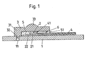
- the transmitting and / or receiving device consists of a base plate 1, an optical chip 2 as a transmitting and / or receiving element, a beam-shaping element 3 and a carrier element 4 for electrical line feeds.
- the base plate 1 is preferably a leadframe or a part of a leadframe whose surface serves as a mounting surface for the further components.
- the optical chip 2 is arranged directly on the base plate 1 or the leadframe. It consists in the illustrated embodiment of an optical transmitting element 21, such as a laser diode or a light emitting diode and an optical receiving element 22, such as a photodiode, which are arranged one above the other in chip-on-chip mounting. Alternatively, only one transmitting element 21 or only one receiving element 22 are provided.
- the transmitting element 21 does not have to be arranged above the receiving element 22.
- the transmitting element and the receiving element can also be arranged side by side on the base plate 1.
- the electrical contacting of the optical chip 2 via arranged on the support member 4 line feeds.
- the carrier 4 which is also fixed directly on the base plate 1, brought close to the optical chip 2.
- the wiring of the support member in turn are contacted via the base plate (not shown) or another electrical Komonente.
- the carrier element 4 is preferably a ceramic plate on which line feeds are designed to be suitable for high frequency.
- the conductor leads are strip conductors.
- the existing ceramic support member 4 with arranged on the top line feeds provides constant high-frequency characteristics even at high frequencies available, as they could not be provided on the base part 1 itself in any case in the case of training as a leadframe.
- edge surfaces of the optical chip 2 and the support member 4 may have the same height with the lead leads as shown. By then located at the same height contact surfaces of the chip 2 and sensible element 4, it is possible to use very short bonding wires or ribbon, whereby the high-frequency properties can be improved.
- the beam-shaping element 3 is connected to the base plate 1 via at least one vertically extending wall 31.
- the base plate has a bore 11 into which a projection 32 of the beam-shaping element 3 engages.
- a plurality of such projections 32 are provided on the circumference of the beam-shaping element, which engage in corresponding bores 11 of the base plate.
- the wall 31 are preferably formed circumferentially except for an opening to be explained, so that the beam-shaping element 3 forms a cavity.
- This cavity constitutes a space 5 between the base plate 1 and the beam-shaping element 3.
- the space has a lateral opening 51, so that the transmitting and / or receiving arrangement is not a hermetically sealed arrangement.
- the opening 51 of the intermediate space 5 on the one hand enables the introduction of the carrier element 4 in the intermediate space 5 to Furthermore, the opening 51 of the intermediate space 5 makes it possible to cast the intermediate space 5 with a transparent encapsulant 6 and, in particular, to encase the optical chip 2 with the encapsulant 6.
- the potting compound is preferably a soft potting compound, for example of silicone.
- the potting compound is relatively soft, so that it exerts no undesirable forces on the optical chip 2. It protects the optical chip 2 from external influences and ensures that it does not get any dirt particles, moisture or the like in the beam path between the optical chip and the beam-shaping element.
- the opening 51 of the gap 5 between the base plate 1 and the beam-forming element 3 remains open even after positioning of the carrier element 4 and introduction of the potting compound 5 and is not closed to compensate for changes in temperature of the potting compound when temperature changes, the due to a temperature coefficient of expansion that changes with temperature.
- the beam-shaping element 3 forms above the optical chip 2 a lens 33 which focuses light emitted by the optical chip 2 onto the end face of an optical waveguide or focuses light emerging from the face of an optical waveguide onto the optical chip, as will be explained with reference to the following figures becomes.
- the bore 11 represents a mechanical structure which, in addition to the attachment of the beam-shaping element 3, also serves for the optical alignment of the further elements, in particular of the optical chip 2.
- a multiplicity of bores 11 are preferably provided, which represent defined markings, that of an image recognition system for placing the optical chip 2 detected on the base plate, compared with an internal coordinate system and evaluated to the effect that the optical chip 2 is placed exactly in the desired position on the base plate 1.
- holes 11 can be used as markings and projections on the base plate.
- the outer shape of the base plate may represent a mark, which serves the mechanical and / or optical alignment of the elements of the transmitting and / or receiving device.
- the adjustment of the optical chip 2 on the base plate 1 instead of by means of an optical image recognition using the illustrated markers 11 can also be effected in that structures are formed on the optical chip, which correspond to corresponding structures on the base plate and accordingly enable a passive alignment or adjustment of the optical chip 2 on the base plate 1. In both cases, no active adjustment of the optical chip 2 is required.
- the beam-shaping element 3 "additionally forms contours 34 'on the side facing away from the base plate 1, by means of which a guide element 71 for an optical waveguide 72 can be coupled to the transmitting and receiving arrangement 71 is, for example, a ferrule which contains the optical waveguide 72 in a central bore
- the contours 34 ' are a cylindrical rim with an internal shoulder 35' which receives the guide element 71.
- Via the lens 33 'of the beam-shaping element is a coupling between the optical waveguide 72 and the optical chip. 2
- a separate coupling element 8 is provided, which serves to receive the guide member 71 with the optical waveguide 72.
- the coupling element 8 is fastened on the base plate 2, for example via prefabricated, corresponding structures on the underside of the coupling element 8 and the mounting surface of the base plate 1. If the base plate and the coupling element are made of metal, after an adjustment, a fastening can also be achieved by a material connection, For example, laser welding done.
- the coupling element 8 has a lateral opening 81 which is aligned with the lateral opening 51 of the intermediate space 5 between the base plate 1 and the beam-shaping element 3.
- the carrier element 4 of the electrical line feeds and the potting compound 9 are thus introduced via the openings 81, 51 in the coupling element 8 and between the base plate 1 and the beam-shaping element 3.
- the coupling element 8 has, in a manner known per se, a bearing surface 83 provided with a window 82 for an optical waveguide 71, 72 to be coupled. It forms below the support surface 83 from a cavity 84 in which the beam-shaping element 3 is located.
- the beam-shaping element 3 is not attached to the base plate 1, but at the bottom of a coupling element 8 'corresponding to the coupling element 8 of Figure 3.
- the lens 33 of the coupling element 3 "into an opening 82 'of the coupling element 8'.
- the opening 82 ' At the opposite end of the opening 82 'are the end faces of the guide member 71 and the optical fiber 72nd
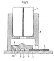
- FIG. 5 shows an exemplary embodiment of a transmitting and / or receiving arrangement in which an amplifier chip 9 is mounted on the base plate 1 in addition to an optical chip 2 'for receiving optical signals (receiver chip). Both the amplifier chip 9 and the receiver chip 2 'are contacted by means of the electrical line feeds of the carrier element 4 and schematically illustrated bond wires. Also, both are within the gap 5 between the base plate 1 and beam-shaping element. 3
- an additional bore 101 is further shown in the base plate 1, which provides a vent and in particular when filling the gap 5 with potting compound is important. Moreover, the structure corresponds to the structure of Figure 3.
- FIG. 6 shows an alternative exemplary embodiment which, except for the feature, corresponds to the exemplary embodiment of FIG. 1 in that the interface 35 "'of the beam-shaping element 3' facing the base plate 1 or the intermediate space 5 does not run parallel to the base plate 1 in a partial region,
- the result is that light emitted from the optical chip 2 is partially reflected at the interface between the gap 5 filled with the potting compound and the beam-shaping element 3 '' and laterally adjacent to the transmitting element 21 on the Receiving element 22 falls whose optically active surface 22a in this embodiment is adjacent to the transmitting element 21.
- it may also be provided to provide a partial mirroring on the oblique surface 35a "'.
- the receiving element 22 is a monitor diode which partially detects the light emitted by the transmitting element 21 and supplies it to a monitoring control loop for regulating the optical power of the transmitting element.
- the monitor diode When forming the transmitting element 21 as a VCSEL laser diode, the modulated laser light emitted vertically upwards, the monitor diode is in an alternative variant directly below the transmitter diode, wherein at the rear surface of the laser resonator, a small amount of light down and coupled to the monitor diode.
Landscapes
- Physics & Mathematics (AREA)
- General Physics & Mathematics (AREA)
- Optics & Photonics (AREA)
- Optical Couplings Of Light Guides (AREA)
Applications Claiming Priority (1)
| Application Number | Priority Date | Filing Date | Title |
|---|---|---|---|
| PCT/DE2001/003603 WO2003027743A1 (de) | 2001-09-14 | 2001-09-14 | Sende- und/oder empfangsanordnung zur optischen signalübertragung |
Publications (2)
| Publication Number | Publication Date |
|---|---|
| EP1425618A1 EP1425618A1 (de) | 2004-06-09 |
| EP1425618B1 true EP1425618B1 (de) | 2006-12-13 |
Family
ID=5648288
Family Applications (1)
| Application Number | Title | Priority Date | Filing Date |
|---|---|---|---|
| EP01978155A Expired - Lifetime EP1425618B1 (de) | 2001-09-14 | 2001-09-14 | Sende- und/oder empfangsanordnung zur optischen signalübertragung |
Country Status (5)
| Country | Link |
|---|---|
| US (1) | US7359646B2 (zh) |
| EP (1) | EP1425618B1 (zh) |
| CN (1) | CN1302306C (zh) |
| DE (1) | DE50111658D1 (zh) |
| WO (1) | WO2003027743A1 (zh) |
Families Citing this family (12)
| Publication number | Priority date | Publication date | Assignee | Title |
|---|---|---|---|---|
| TW579071U (en) * | 2002-02-26 | 2004-03-01 | Ind Tech Res Inst | Optoelectronic module package |
| FR2871583A1 (fr) * | 2004-06-14 | 2005-12-16 | Commissariat Energie Atomique | Dispositif de prelevement d'une partie d'un faisceau lumineux issu d'un composant electronique emetteur de lumiere |
| GB2428103B (en) * | 2005-07-07 | 2009-06-17 | Agilent Technologies Inc | An optical device |
| TW200903852A (en) * | 2007-07-11 | 2009-01-16 | Everlight Electronics Co Ltd | Fabricating method for lens of LED device and apparatus thereof |
| US8265487B2 (en) * | 2009-07-29 | 2012-09-11 | Avago Technologies Fiber Ip (Singapore) Pte. Ltd. | Half-duplex, single-fiber (S-F) optical transceiver module and method |
| CN102736199B (zh) * | 2012-05-23 | 2014-10-22 | 日月光半导体制造股份有限公司 | 光耦合模块构造 |
| US9129578B2 (en) * | 2012-09-28 | 2015-09-08 | Innocom Technology (Shenzhen) Co., Ltd. | Shift register circuit and display device using the same |
| JP6518113B2 (ja) * | 2015-04-10 | 2019-05-22 | ヒロセ電機株式会社 | 光電気変換コネクタ及びその製造方法 |
| US10295768B2 (en) * | 2016-07-08 | 2019-05-21 | Finisar Corporation | Chip on leadframe optical subassembly |
| US10866373B2 (en) * | 2018-06-27 | 2020-12-15 | Taiwan Semiconductor Manufacturing Company, Ltd. | Optical transceiver and manufacturing method thereof |
| TWI700838B (zh) * | 2019-05-07 | 2020-08-01 | 喆光照明光電股份有限公司 | 以二次封膠成型之層疊光耦合器及其封裝方法 |
| JP7400602B2 (ja) * | 2020-04-01 | 2023-12-19 | 住友電気工業株式会社 | 光レセプタクル |
Family Cites Families (12)
| Publication number | Priority date | Publication date | Assignee | Title |
|---|---|---|---|---|
| JPS5977402A (ja) * | 1982-10-26 | 1984-05-02 | Toshiba Corp | 光リンク |
| JPS59220982A (ja) * | 1983-05-31 | 1984-12-12 | Sumitomo Electric Ind Ltd | 光素子用パッケ−ジ |
| US5093879A (en) * | 1990-06-22 | 1992-03-03 | International Business Machines Corporation | Electro-optical connectors |
| JP2792722B2 (ja) * | 1990-07-16 | 1998-09-03 | 三菱電機株式会社 | 半導体発光装置 |
| JP3047735B2 (ja) * | 1994-05-16 | 2000-06-05 | 住友電気工業株式会社 | 光受信モジュ−ルとその製造方法 |
| DE19508222C1 (de) * | 1995-03-08 | 1996-06-05 | Siemens Ag | Optoelektronischer Wandler und Herstellverfahren |
| JP3191729B2 (ja) | 1997-07-03 | 2001-07-23 | 日本電気株式会社 | 光半導体モジュールとその製造方法 |
| DE29813985U1 (de) * | 1998-08-05 | 1998-10-29 | Leopold Kostal GmbH & Co KG, 58507 Lüdenscheid | Vergußkapselung für einen auf einer Leiterbahnstruktur aufgesetzten Halbleiterbaustein sowie Halbleiterbaustein mit einer solchen Vergußkapselung |
| CA2367362C (en) * | 1999-03-19 | 2004-11-09 | Cielo Communications, Inc. | Vcsel power monitoring system using plastic encapsulation techniques |
| JP2001174671A (ja) * | 1999-12-16 | 2001-06-29 | Japan Aviation Electronics Industry Ltd | 光素子モジュール |
| DE10004411A1 (de) * | 2000-02-02 | 2001-08-16 | Infineon Technologies Ag | Elektrooptisches Sende-/Empfangsmodul und Verfahren zu seiner Herstellung |
| US6873799B2 (en) * | 2001-06-20 | 2005-03-29 | Jds Uniphase Corporation | Optical subassembly for optical communications |
-
2001
- 2001-09-14 EP EP01978155A patent/EP1425618B1/de not_active Expired - Lifetime
- 2001-09-14 WO PCT/DE2001/003603 patent/WO2003027743A1/de active IP Right Grant
- 2001-09-14 DE DE50111658T patent/DE50111658D1/de not_active Expired - Lifetime
- 2001-09-14 US US10/489,683 patent/US7359646B2/en not_active Expired - Fee Related
- 2001-09-14 CN CNB018236340A patent/CN1302306C/zh not_active Expired - Fee Related
Also Published As
| Publication number | Publication date |
|---|---|
| US20050036732A1 (en) | 2005-02-17 |
| EP1425618A1 (de) | 2004-06-09 |
| CN1547678A (zh) | 2004-11-17 |
| US7359646B2 (en) | 2008-04-15 |
| CN1302306C (zh) | 2007-02-28 |
| WO2003027743A1 (de) | 2003-04-03 |
| DE50111658D1 (de) | 2007-01-25 |
Similar Documents
| Publication | Publication Date | Title |
|---|---|---|
| DE102004064081B4 (de) | Gehäuse für einen optischen Empfänger | |
| EP1425618B1 (de) | Sende- und/oder empfangsanordnung zur optischen signalübertragung | |
| DE69907351T2 (de) | Photodiodenmodul | |
| DE69700230T2 (de) | Laserlichtquelle | |
| DE60029807T2 (de) | Optoelektronische module mit doppelter umhüllung | |
| DE10065624C2 (de) | Kopplungsanordnung zum optischen Koppeln eines Lichtwellenleiters mit einem elektro-optischen oder opto-elektrischen Halbleiterwandler | |
| DE69421767T2 (de) | Optoelektronische Hybridintegrationsplattform, optisches Untermodul, optoelektronische hybridintegrierte Schaltung, und Herstellungsverfahren der Plattform | |
| DE68929065T2 (de) | Unterbaugruppe für optoelektronische Bauelemente | |
| DE19640423C1 (de) | Optoelektronisches Modul zur bidirektionalen optischen Datenübertragung | |
| US20100151614A1 (en) | Wafer level method of forming side fiber insertion optoelectronic packages | |
| EP0111263B1 (de) | Sende- oder Empfangsvorrichtung mit einer mittels eines Trägers gehalterten Diode | |
| WO2012031781A2 (de) | Optoelektronisches bauelement | |
| DE19935496C1 (de) | Optoelektronisches Bauelement und Verfahren zur Herstellung | |
| WO2012031780A2 (de) | Optoelektronisches bauelement | |
| DE10322757B4 (de) | Optoelektronische Sende- und/oder Empfangsanordnungen | |
| DE69833611T2 (de) | Ein Mikro-Photonikmodul mit einer Trennwand | |
| DE19616969A1 (de) | Optische Baugruppe zur Ankopplung eines Lichtwellenleiters und Verfahren zur Herstellung derselben | |
| DE102004025661B4 (de) | Optische-Vorrichtung -Gehäuse mit Drehspiegel und Ausrichtungspfosten | |
| DE102006061722B4 (de) | Anschlussmodul und Verfahren zum Herstellen desselben | |
| CN103185933B (zh) | 光学基板、光学基板的制造方法以及光学模块结构 | |
| DE19640421A1 (de) | Optoelektronisches Modul zur bidirektionalen optischen Datenübertragung | |
| US20050254745A1 (en) | Optoelectronic module and optoelectronic system | |
| US20050189548A1 (en) | Optical transmission module | |
| DE19635583A1 (de) | Optoelektronisches Sende- und/oder Empfangsmodul | |
| DE19963262A1 (de) | Wandlermodul mit einem Optohalbleiter und Verfahren zur Herstellung eines solchen Wandlermoduls |
Legal Events
| Date | Code | Title | Description |
|---|---|---|---|
| PUAI | Public reference made under article 153(3) epc to a published international application that has entered the european phase |
Free format text: ORIGINAL CODE: 0009012 |
|
| 17P | Request for examination filed |
Effective date: 20040302 |
|
| AK | Designated contracting states |
Kind code of ref document: A1 Designated state(s): AT BE CH CY DE DK ES FI FR GB GR IE IT LI LU MC NL PT SE TR |
|
| AX | Request for extension of the european patent |
Extension state: AL LT LV MK RO SI |
|
| 17Q | First examination report despatched |
Effective date: 20040923 |
|
| GRAP | Despatch of communication of intention to grant a patent |
Free format text: ORIGINAL CODE: EPIDOSNIGR1 |
|
| RAP1 | Party data changed (applicant data changed or rights of an application transferred) |
Owner name: FINISAR CORPORATION |
|
| GRAS | Grant fee paid |
Free format text: ORIGINAL CODE: EPIDOSNIGR3 |
|
| GRAA | (expected) grant |
Free format text: ORIGINAL CODE: 0009210 |
|
| AK | Designated contracting states |
Kind code of ref document: B1 Designated state(s): DE FR GB |
|
| RBV | Designated contracting states (corrected) |
Designated state(s): DE FR GB |
|
| REG | Reference to a national code |
Ref country code: GB Ref legal event code: FG4D Free format text: NOT ENGLISH |
|
| REF | Corresponds to: |
Ref document number: 50111658 Country of ref document: DE Date of ref document: 20070125 Kind code of ref document: P |
|
| GBT | Gb: translation of ep patent filed (gb section 77(6)(a)/1977) |
Effective date: 20070307 |
|
| ET | Fr: translation filed | ||
| PLBE | No opposition filed within time limit |
Free format text: ORIGINAL CODE: 0009261 |
|
| STAA | Information on the status of an ep patent application or granted ep patent |
Free format text: STATUS: NO OPPOSITION FILED WITHIN TIME LIMIT |
|
| 26N | No opposition filed |
Effective date: 20070914 |
|
| PGFP | Annual fee paid to national office [announced via postgrant information from national office to epo] |
Ref country code: FR Payment date: 20140917 Year of fee payment: 14 Ref country code: GB Payment date: 20140929 Year of fee payment: 14 |
|
| PGFP | Annual fee paid to national office [announced via postgrant information from national office to epo] |
Ref country code: DE Payment date: 20140929 Year of fee payment: 14 |
|
| REG | Reference to a national code |
Ref country code: DE Ref legal event code: R119 Ref document number: 50111658 Country of ref document: DE |
|
| GBPC | Gb: european patent ceased through non-payment of renewal fee |
Effective date: 20150914 |
|
| REG | Reference to a national code |
Ref country code: FR Ref legal event code: ST Effective date: 20160531 |
|
| PG25 | Lapsed in a contracting state [announced via postgrant information from national office to epo] |
Ref country code: GB Free format text: LAPSE BECAUSE OF NON-PAYMENT OF DUE FEES Effective date: 20150914 Ref country code: DE Free format text: LAPSE BECAUSE OF NON-PAYMENT OF DUE FEES Effective date: 20160401 |
|
| PG25 | Lapsed in a contracting state [announced via postgrant information from national office to epo] |
Ref country code: FR Free format text: LAPSE BECAUSE OF NON-PAYMENT OF DUE FEES Effective date: 20150930 |