EP1425618B1 - Transmitter and/or receiver arrangement for optical signal transmission - Google Patents
Transmitter and/or receiver arrangement for optical signal transmission Download PDFInfo
- Publication number
- EP1425618B1 EP1425618B1 EP01978155A EP01978155A EP1425618B1 EP 1425618 B1 EP1425618 B1 EP 1425618B1 EP 01978155 A EP01978155 A EP 01978155A EP 01978155 A EP01978155 A EP 01978155A EP 1425618 B1 EP1425618 B1 EP 1425618B1
- Authority
- EP
- European Patent Office
- Prior art keywords
- transmitting
- base plate
- receiving
- arrangement according
- receiving arrangement
- Prior art date
- Legal status (The legal status is an assumption and is not a legal conclusion. Google has not performed a legal analysis and makes no representation as to the accuracy of the status listed.)
- Expired - Lifetime
Links
Images


Classifications
-
- G—PHYSICS
- G02—OPTICS
- G02B—OPTICAL ELEMENTS, SYSTEMS OR APPARATUS
- G02B6/00—Light guides; Structural details of arrangements comprising light guides and other optical elements, e.g. couplings
- G02B6/24—Coupling light guides
- G02B6/42—Coupling light guides with opto-electronic elements
- G02B6/4201—Packages, e.g. shape, construction, internal or external details
- G02B6/4219—Mechanical fixtures for holding or positioning the elements relative to each other in the couplings; Alignment methods for the elements, e.g. measuring or observing methods especially used therefor
- G02B6/4228—Passive alignment, i.e. without a detection of the degree of coupling or the position of the elements
- G02B6/423—Passive alignment, i.e. without a detection of the degree of coupling or the position of the elements using guiding surfaces for the alignment
-
- G—PHYSICS
- G02—OPTICS
- G02B—OPTICAL ELEMENTS, SYSTEMS OR APPARATUS
- G02B6/00—Light guides; Structural details of arrangements comprising light guides and other optical elements, e.g. couplings
- G02B6/24—Coupling light guides
- G02B6/42—Coupling light guides with opto-electronic elements
- G02B6/4201—Packages, e.g. shape, construction, internal or external details
- G02B6/4204—Packages, e.g. shape, construction, internal or external details the coupling comprising intermediate optical elements, e.g. lenses, holograms
-
- G—PHYSICS
- G02—OPTICS
- G02B—OPTICAL ELEMENTS, SYSTEMS OR APPARATUS
- G02B6/00—Light guides; Structural details of arrangements comprising light guides and other optical elements, e.g. couplings
- G02B6/24—Coupling light guides
- G02B6/42—Coupling light guides with opto-electronic elements
- G02B6/4201—Packages, e.g. shape, construction, internal or external details
- G02B6/4274—Electrical aspects
- G02B6/4279—Radio frequency signal propagation aspects of the electrical connection, high frequency adaptations
-
- G—PHYSICS
- G02—OPTICS
- G02B—OPTICAL ELEMENTS, SYSTEMS OR APPARATUS
- G02B6/00—Light guides; Structural details of arrangements comprising light guides and other optical elements, e.g. couplings
- G02B6/24—Coupling light guides
- G02B6/42—Coupling light guides with opto-electronic elements
- G02B6/4201—Packages, e.g. shape, construction, internal or external details
-
- H—ELECTRICITY
- H01—ELECTRIC ELEMENTS
- H01L—SEMICONDUCTOR DEVICES NOT COVERED BY CLASS H10
- H01L2224/00—Indexing scheme for arrangements for connecting or disconnecting semiconductor or solid-state bodies and methods related thereto as covered by H01L24/00
- H01L2224/01—Means for bonding being attached to, or being formed on, the surface to be connected, e.g. chip-to-package, die-attach, "first-level" interconnects; Manufacturing methods related thereto
- H01L2224/42—Wire connectors; Manufacturing methods related thereto
- H01L2224/47—Structure, shape, material or disposition of the wire connectors after the connecting process
- H01L2224/48—Structure, shape, material or disposition of the wire connectors after the connecting process of an individual wire connector
- H01L2224/4805—Shape
- H01L2224/4809—Loop shape
- H01L2224/48091—Arched
Definitions
- the invention relates to a transmitting and / or receiving arrangement for optical signal transmission according to the preamble of claim 1.
- optical communication transmission and / or receiving arrangements are used to couple light signals in a waveguide and / or to detect optical signals received by a waveguide.
- compact and cost-effective transmission and / or reception arrangements are required both for multimode optical waveguides and for single-mode optical waveguides.
- TO packages are well-known in the art standard housing for optical transmitting or receiving elements whose shape is similar to the housing of a (classic) transistor, but at the top of a glass window for light entrance and exit. The signal is supplied via contact pins, which are led away from the TO housing down.
- Transmitting and / or receiving arrangements for optical signal transmission with TO housing have the disadvantage that they are only limited high frequency suitable. Their use in the frequency range of several Gbit / s and more is only possible with special customization of the electronics.
- transmission and / or receiving arrangements are known in the prior art, in which special, hermetically sealed high frequency housing are provided which allow lateral passage of the optical waveguide or optical beam.
- high frequency housing with lateral implementation are very complicated and expensive.
- the present invention seeks to provide a transmitting and / or receiving device for optical signal transmission available that can be used with a simple and inexpensive construction even at high data rates above 1 Gbit / s.
- the invention provides that the electrical leads are arranged on a support member fixed to the base plate, which extends at least partially into the space between the base plate and the beam-shaping element, wherein the support member with the electrical line feeds close to the optical transmitting and / or Receiving element is introduced while partially filling a side opening, which has the gap.
- the intermediate space is limited by the base plate, the beam-shaping element and at least one lateral boundary, which is formed by the beam-shaping element or a coupling element for coupling a waveguide.
- the lateral opening is formed in a region of the gap in which the gap has no lateral boundary.
- Non-hermetic packaging associated with a special arrangement of the necessary components of a transmitting and / or receiving arrangement.
- Non-hermetic is understood to mean that there is no encapsulation of the transmitting and / or receiving arrangement caused by soldering, welding, blowing, etc.
- the non-hermetic construction or the provision of at least one opening of the intermediate space between the Base plate and the beam-shaping element makes it possible to introduce the carrier element with the electrical line feeds close to the optical transmitting and / or receiving element.
- the support element partially fills the lateral opening.
- a lateral opening of the gap between the base plate and the beam-shaping element it is possible, after the individual components have been arranged on the base plate, to introduce a potting material into the intermediate space.
- the one surface of the base plate serves as a mounting surface for the other components. This allows a simpler, cheaper construction.
- the formation of a gap allows the protected arrangement of components on the base plate close to the transmitting and / or receiving arrangement.
- a transparent potting compound in the space between the base plate and the beam-shaping element, which completely fills the optical beam path between the transmitting and / or receiving element and the beam-shaping element.
- the transmitting and / or receiving element and associated contact lines are completely enclosed by the potting compound to protect them.
- potting material while a soft casting is preferably used, such as a silicone compound, so that no forces are exerted by the potting compound on the transmitting and / or receiving element.
- the potting compound serves to protect the transmitting and / or receiving element and the beam path from external influences such as dirt and moisture.
- the base plate has mechanical structures for mechanical and / or optical alignment of the elements arranged thereon.
- the mechanical structures are, for example, holes in the base plate, around elevations, or around a specially shaped outer contour of the base plate or of parts of the base plate.
- the mechanical structures of the base plate allow precise alignment of the transmitting and / or receiving element on the base plate. This can be done via optical image recognition methods, the mechanical contours serving as markers for image recognition. At least two such contours or markings are preferably provided.
- image recognition method for exact positioning and adjustment of the transmitting and / or receiving element 2 may alternatively be provided that on the transmitting and / or receiving element corresponding mechanical structures are formed, so that by means of the corresponding structures, a passive adjustment between transmitting and / or receiving element and the base plate takes place.
- the mechanical structures of the base plate serve to align and secure the beam-shaping element.
- the beam-shaping element preferably has mechanical structures on the side facing the base plate which serve for the optical and / or mechanical alignment of the beam-shaping element when placed on the base plate.
- the beam-shaping element has projections which engage in corresponding bores of the base plate, whereby the beam-shaping element is fastened and adjusted simultaneously on the base plate. An additional attachment by adhesive, etc. is of course possible and possibly useful.
- the beam-forming element connected to the base plate faces on the base plate Side a cavity which forms the gap between the base plate and the beam-shaping element and which provides the at least one lateral boundary of the gap.
- the beam-shaping element is a kind of protective covering of the transmitting and / or receiving element.
- At least one further opening is preferably present, which is formed for example by a bore in the base plate or in the beam-shaping element.
- Such a further opening constitutes a vent opening when filling a potting compound into the intermediate space and facilitates the filling of the intermediate space with potting compound.
- the lateral opening is preferably not closed because it serves to compensate for temperature-induced expansion variations of the transparent potting material.
- the carrier element with the electrical line feeders is a ceramic, in particular a ceramic plate made of nonconductive material, on whose upper side the line feeders are formed.
- the cable leads are preferably formed in high-frequency technology, such as stripline.
- Corresponding ceramic parts can be produced with high precision and low fluctuations in their HF properties. Therefore, by using a ceramic as a carrier of the electrical line feeders, it is possible to provide strip conductors with precisely defined, constant and reproducible high-frequency properties.
- the beam-shaping element faces away from the base plate Contours for coupling an optical waveguide.
- contours are not formed on the beam-shaping element, but on a separate coupling element which is connected as a separate part with the base plate.
- the coupling element also has a lateral opening in order not to close the intermediate space between the base plate and the beam-shaping element.
- the beam-shaping element may be attached to the additional coupling element instead of the base plate, in which case of course the latter is connected to the base plate and forms the lateral boundary of the intermediate space.
- a monitor diode can be arranged below or next to the transmitting and / or receiving element. If a monitor diode is located next to the transmitting and / or receiving element, it is provided in a special embodiment of the invention to form the boundary surface of the beam-shaping element obliquely to the intermediate space at least in a region, so that a part of the radiation emitted by the transmitting element at the oblique reflected surface running back and thus directed to the arranged next to the transmitting element monitor diode.
- the oblique position also prevents radiation emitted by the transmitting element from being returned to the transmitting element.
- To increase the reflected radiation can be provided on the inclined portion of the interface to apply a partially transparent or partially reflecting mirror layer.
- the baseplate is preferably a leadframe or part of a leadframe, which has the advantage of simple and inexpensive production using standard techniques. On the leadframe, the individual components of the transmitting and / or receiving arrangement are fastened or aligned in the manner described.
- the base plate consists of a planar substrate, for example a silicon substrate.
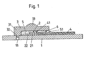
- the transmitting and / or receiving device consists of a base plate 1, an optical chip 2 as a transmitting and / or receiving element, a beam-shaping element 3 and a carrier element 4 for electrical line feeds.
- the base plate 1 is preferably a leadframe or a part of a leadframe whose surface serves as a mounting surface for the further components.
- the optical chip 2 is arranged directly on the base plate 1 or the leadframe. It consists in the illustrated embodiment of an optical transmitting element 21, such as a laser diode or a light emitting diode and an optical receiving element 22, such as a photodiode, which are arranged one above the other in chip-on-chip mounting. Alternatively, only one transmitting element 21 or only one receiving element 22 are provided.
- the transmitting element 21 does not have to be arranged above the receiving element 22.
- the transmitting element and the receiving element can also be arranged side by side on the base plate 1.
- the electrical contacting of the optical chip 2 via arranged on the support member 4 line feeds.
- the carrier 4 which is also fixed directly on the base plate 1, brought close to the optical chip 2.
- the wiring of the support member in turn are contacted via the base plate (not shown) or another electrical Komonente.
- the carrier element 4 is preferably a ceramic plate on which line feeds are designed to be suitable for high frequency.
- the conductor leads are strip conductors.
- the existing ceramic support member 4 with arranged on the top line feeds provides constant high-frequency characteristics even at high frequencies available, as they could not be provided on the base part 1 itself in any case in the case of training as a leadframe.
- edge surfaces of the optical chip 2 and the support member 4 may have the same height with the lead leads as shown. By then located at the same height contact surfaces of the chip 2 and sensible element 4, it is possible to use very short bonding wires or ribbon, whereby the high-frequency properties can be improved.
- the beam-shaping element 3 is connected to the base plate 1 via at least one vertically extending wall 31.
- the base plate has a bore 11 into which a projection 32 of the beam-shaping element 3 engages.
- a plurality of such projections 32 are provided on the circumference of the beam-shaping element, which engage in corresponding bores 11 of the base plate.
- the wall 31 are preferably formed circumferentially except for an opening to be explained, so that the beam-shaping element 3 forms a cavity.
- This cavity constitutes a space 5 between the base plate 1 and the beam-shaping element 3.
- the space has a lateral opening 51, so that the transmitting and / or receiving arrangement is not a hermetically sealed arrangement.
- the opening 51 of the intermediate space 5 on the one hand enables the introduction of the carrier element 4 in the intermediate space 5 to Furthermore, the opening 51 of the intermediate space 5 makes it possible to cast the intermediate space 5 with a transparent encapsulant 6 and, in particular, to encase the optical chip 2 with the encapsulant 6.
- the potting compound is preferably a soft potting compound, for example of silicone.
- the potting compound is relatively soft, so that it exerts no undesirable forces on the optical chip 2. It protects the optical chip 2 from external influences and ensures that it does not get any dirt particles, moisture or the like in the beam path between the optical chip and the beam-shaping element.
- the opening 51 of the gap 5 between the base plate 1 and the beam-forming element 3 remains open even after positioning of the carrier element 4 and introduction of the potting compound 5 and is not closed to compensate for changes in temperature of the potting compound when temperature changes, the due to a temperature coefficient of expansion that changes with temperature.
- the beam-shaping element 3 forms above the optical chip 2 a lens 33 which focuses light emitted by the optical chip 2 onto the end face of an optical waveguide or focuses light emerging from the face of an optical waveguide onto the optical chip, as will be explained with reference to the following figures becomes.
- the bore 11 represents a mechanical structure which, in addition to the attachment of the beam-shaping element 3, also serves for the optical alignment of the further elements, in particular of the optical chip 2.
- a multiplicity of bores 11 are preferably provided, which represent defined markings, that of an image recognition system for placing the optical chip 2 detected on the base plate, compared with an internal coordinate system and evaluated to the effect that the optical chip 2 is placed exactly in the desired position on the base plate 1.
- holes 11 can be used as markings and projections on the base plate.
- the outer shape of the base plate may represent a mark, which serves the mechanical and / or optical alignment of the elements of the transmitting and / or receiving device.
- the adjustment of the optical chip 2 on the base plate 1 instead of by means of an optical image recognition using the illustrated markers 11 can also be effected in that structures are formed on the optical chip, which correspond to corresponding structures on the base plate and accordingly enable a passive alignment or adjustment of the optical chip 2 on the base plate 1. In both cases, no active adjustment of the optical chip 2 is required.
- the beam-shaping element 3 "additionally forms contours 34 'on the side facing away from the base plate 1, by means of which a guide element 71 for an optical waveguide 72 can be coupled to the transmitting and receiving arrangement 71 is, for example, a ferrule which contains the optical waveguide 72 in a central bore
- the contours 34 ' are a cylindrical rim with an internal shoulder 35' which receives the guide element 71.
- Via the lens 33 'of the beam-shaping element is a coupling between the optical waveguide 72 and the optical chip. 2
- a separate coupling element 8 is provided, which serves to receive the guide member 71 with the optical waveguide 72.
- the coupling element 8 is fastened on the base plate 2, for example via prefabricated, corresponding structures on the underside of the coupling element 8 and the mounting surface of the base plate 1. If the base plate and the coupling element are made of metal, after an adjustment, a fastening can also be achieved by a material connection, For example, laser welding done.
- the coupling element 8 has a lateral opening 81 which is aligned with the lateral opening 51 of the intermediate space 5 between the base plate 1 and the beam-shaping element 3.
- the carrier element 4 of the electrical line feeds and the potting compound 9 are thus introduced via the openings 81, 51 in the coupling element 8 and between the base plate 1 and the beam-shaping element 3.
- the coupling element 8 has, in a manner known per se, a bearing surface 83 provided with a window 82 for an optical waveguide 71, 72 to be coupled. It forms below the support surface 83 from a cavity 84 in which the beam-shaping element 3 is located.
- the beam-shaping element 3 is not attached to the base plate 1, but at the bottom of a coupling element 8 'corresponding to the coupling element 8 of Figure 3.
- the lens 33 of the coupling element 3 "into an opening 82 'of the coupling element 8'.
- the opening 82 ' At the opposite end of the opening 82 'are the end faces of the guide member 71 and the optical fiber 72nd
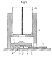
- FIG. 5 shows an exemplary embodiment of a transmitting and / or receiving arrangement in which an amplifier chip 9 is mounted on the base plate 1 in addition to an optical chip 2 'for receiving optical signals (receiver chip). Both the amplifier chip 9 and the receiver chip 2 'are contacted by means of the electrical line feeds of the carrier element 4 and schematically illustrated bond wires. Also, both are within the gap 5 between the base plate 1 and beam-shaping element. 3
- an additional bore 101 is further shown in the base plate 1, which provides a vent and in particular when filling the gap 5 with potting compound is important. Moreover, the structure corresponds to the structure of Figure 3.
- FIG. 6 shows an alternative exemplary embodiment which, except for the feature, corresponds to the exemplary embodiment of FIG. 1 in that the interface 35 "'of the beam-shaping element 3' facing the base plate 1 or the intermediate space 5 does not run parallel to the base plate 1 in a partial region,
- the result is that light emitted from the optical chip 2 is partially reflected at the interface between the gap 5 filled with the potting compound and the beam-shaping element 3 '' and laterally adjacent to the transmitting element 21 on the Receiving element 22 falls whose optically active surface 22a in this embodiment is adjacent to the transmitting element 21.
- it may also be provided to provide a partial mirroring on the oblique surface 35a "'.
- the receiving element 22 is a monitor diode which partially detects the light emitted by the transmitting element 21 and supplies it to a monitoring control loop for regulating the optical power of the transmitting element.
- the monitor diode When forming the transmitting element 21 as a VCSEL laser diode, the modulated laser light emitted vertically upwards, the monitor diode is in an alternative variant directly below the transmitter diode, wherein at the rear surface of the laser resonator, a small amount of light down and coupled to the monitor diode.
Abstract
Description
Die Erfindung betrifft eine Sende- und/oder Empfangsanordnung zur optischen Signalübertragung gemäß dem Oberbegriff des Anspruchs 1.The invention relates to a transmitting and / or receiving arrangement for optical signal transmission according to the preamble of
In der optischen Nachrichtenübertragung werden Sende- und/oder Empfangsanordnungen eingesetzt, um Lichtsignale in einen Wellenleiter einzukoppeln und/oder von einem Wellenleiter empfangene optische Signale zu detektieren. Für Anwendungen in der Datenkommunikation werden sowohl für Multimode-Lichtwellenleiter als auch für Singlemode-Lichtwellenleiter kompakte und kostengünstige Sende- und/oder Empfangsanordnungen benötigt.In optical communication transmission and / or receiving arrangements are used to couple light signals in a waveguide and / or to detect optical signals received by a waveguide. For applications in data communication, compact and cost-effective transmission and / or reception arrangements are required both for multimode optical waveguides and for single-mode optical waveguides.
Es sind aus der gatttungsgemäßen EP 0 684 651 A2 Sende- und/oder Empfangsanordnungen bekannt, bei denen ein Sende- und/oder Empfangselement hermetisch dicht in einem sogenannten TO-Gehäuse angeordnet ist. TO-Gehäuse sind im Stand der Technik bekannte Standardgehäuse für optische Sende- oder Empfangselemente, deren Form dem Gehäuse eines (klassischen) Transistors ähnelt, die jedoch an der Oberseite ein Glasfenster zum Lichtein- und -austritt aufweisen. Die Signalzuführung erfolgt über Kontaktpins, die nach unten von dem TO-Gehäuse weggeführt sind. Sende- und/oder Empfangsanordnungen zur optischen Signalübertragung mit TO-Gehäuse weisen den Nachteil auf, daß sie nur begrenzt hochfrequenzgeeignet sind. Ihr Einsatz im Frequenzbereich von einigen Gbit/s und mehr ist nur noch bei spezieller individueller Anpassung der Elektronik möglich.There are known from the generic EP 0 684 651 A2 transmitting and / or receiving arrangements in which a transmitting and / or receiving element is arranged hermetically sealed in a so-called TO-housing. TO packages are well-known in the art standard housing for optical transmitting or receiving elements whose shape is similar to the housing of a (classic) transistor, but at the top of a glass window for light entrance and exit. The signal is supplied via contact pins, which are led away from the TO housing down. Transmitting and / or receiving arrangements for optical signal transmission with TO housing have the disadvantage that they are only limited high frequency suitable. Their use in the frequency range of several Gbit / s and more is only possible with special customization of the electronics.
Des weiteren sind im Stand der Technik Sende- und/oder Empfangsanordnungen bekannt, bei denen spezielle, hermetisch dichte Hochfrequenzgehäuse vorgesehen sind, die eine seitliche Durchführung des optischen Wellenleiters oder optischen Strahls erlauben. Derartige Hochfrequenzgehäuse mit seitlicher Durchführung sind sehr aufwendig und teuer.Furthermore, transmission and / or receiving arrangements are known in the prior art, in which special, hermetically sealed high frequency housing are provided which allow lateral passage of the optical waveguide or optical beam. Such high frequency housing with lateral implementation are very complicated and expensive.
Ausgehend von diesem Stand der Technik liegt der vorliegenden Erfindung die Aufgabe zugrunde, eine Sende- und/oder Empfangsanordnung zur optischen Signalübertragung zur Verfügung zu stellen, die bei einfachem und kostengünstigen Aufbau auch bei hohen Datenraten oberhalb von 1 Gbit/s eingesetzt werden kann.Based on this prior art, the present invention seeks to provide a transmitting and / or receiving device for optical signal transmission available that can be used with a simple and inexpensive construction even at high data rates above 1 Gbit / s.
Diese Aufgabe wird erfindungsgemäß durch eine Sende- und/oder Empfangsanordnung mit den Merkmalen des Anspruchs 1 gelöst. Vorteilhafte und bevorzugte Ausgestaltungen der Erfindung sind in den Unteransprüchen angegeben.This object is achieved by a transmitting and / or receiving device having the features of
Danach ist erfindungsgemäß vorgesehen, daß die elektrischen Zuführungen auf einem auf der Basisplatte befestigten Trägerelement angeordnet sind, das sich zumindest teilweise in den Zwischenraum zwischen der Basisplatte und dem Strahlformungselement erstreckt, wobei das Trägerelement mit den elektrischen Leitungszuführungen dicht an das optische Sende- und/oder Empfangselement herangeführt ist und dabei eine seitliche Öffnung teilweise ausfüllt, die der Zwischenraum aufweist. Der Zwischenraum ist dabei durch die Basisplatte, das Strahlformungselement und mindestens eine seitliche Begrenzung begrenzt, die durch das Strahlformungselement oder ein Koppelelement zur Ankopplung eines Wellenleiters gebildet ist. Die seitliche Öffnung ist in einem Bereich des Zwischenraums ausgebildet, in dem der Zwischenraum keine seitliche Begrenzung aufweist.Thereafter, the invention provides that the electrical leads are arranged on a support member fixed to the base plate, which extends at least partially into the space between the base plate and the beam-shaping element, wherein the support member with the electrical line feeds close to the optical transmitting and / or Receiving element is introduced while partially filling a side opening, which has the gap. The intermediate space is limited by the base plate, the beam-shaping element and at least one lateral boundary, which is formed by the beam-shaping element or a coupling element for coupling a waveguide. The lateral opening is formed in a region of the gap in which the gap has no lateral boundary.
Es liegt ein nicht hermetisches Packaging verbunden mit einer speziellen Anordnung der notwendigen Komponenten einer Sende- und/oder Empfangsanordnung vor. Unter nicht hermetisch wird dabei verstanden, daß keine durch Löten, Verschweißen, Einglasen etc. herbeigeführte Abkapselung der Sende- und/oder Empfangsanordnung vorliegt.There is a non-hermetic packaging associated with a special arrangement of the necessary components of a transmitting and / or receiving arrangement. Non-hermetic is understood to mean that there is no encapsulation of the transmitting and / or receiving arrangement caused by soldering, welding, blowing, etc.
Der nicht hermetische Aufbau bzw. das Zurverfügungstellen mindestens einer Öffnung des Zwischenraums zwischen der Basisplatte und dem Strahlformungselement erlaubt es, das Trägerelement mit den elektrischen Leitungszuführungen dicht an das optische Sende- und/oder Empfangselement heranzuführen. Dabei füllt das Trägerelement die seitliche Öffnung teilweise aus. Auch besteht durch das Vorhandensein einer seitlichen Öffnung des Zwischenraums zwischen Basisplatte und Strahlformungselement die Möglichkeit, nach Anordnung der einzelnen Komponenten auf der Basisplatte ein Vergußmaterial in den Zwischenraum einzubringen.The non-hermetic construction or the provision of at least one opening of the intermediate space between the Base plate and the beam-shaping element makes it possible to introduce the carrier element with the electrical line feeds close to the optical transmitting and / or receiving element. In this case, the support element partially fills the lateral opening. Also, by the presence of a lateral opening of the gap between the base plate and the beam-shaping element, it is possible, after the individual components have been arranged on the base plate, to introduce a potting material into the intermediate space.
Es wird somit eine spezielle Anordnung der notwendigen Komponenten einer Sende- und/oder Empfangsanordnung bereitgestellt. Dabei dient die eine Oberfläche der Basisplatte als Montagefläche für die weiteren Komponenten. Dies erlaubt einen einfacheren, kostengünstigeren Aufbau. Die Ausbildung eines Zwischenraums ermöglicht die geschützte Anordnung von Komponenten auf der Basisplatte nahe an der Sende- und/oder Empfangsanordnung.Thus, a special arrangement of the necessary components of a transmitting and / or receiving arrangement is provided. The one surface of the base plate serves as a mounting surface for the other components. This allows a simpler, cheaper construction. The formation of a gap allows the protected arrangement of components on the base plate close to the transmitting and / or receiving arrangement.
In einer bevorzugten Ausgestaltung der Erfindung ist vorgesehen, in den Zwischenraum zwischen der Basisplatte und dem Strahlformungselement zumindest teilweise eine transparente Vergußmasse einzubringen, die den optischen Strahlengang zwischen dem Sende- und/oder Empfangselement und dem Strahlformungselement vollständig ausfüllt. Vorteilhafterweise sind auch das Sende- und/oder Empfangselement und zugehörige Kontaktleitungen von der Vergußmasse vollständig umschlossen, um sie zu schützen. Als Vergußmaterial wird dabei bevorzugt ein weicher Verguß verwendet, etwa eine Silikonmasse, damit keine Kräfte von der Vergußmasse auf das Sende- und/oder Empfangselement ausgeübt werden. Die Vergußmasse dient einem Schutz des Sende- und/oder Empfangselementes sowie des Strahlengangs gegenüber äußeren Einflüssen wie Schmutz und Feuchtigkeit.In a preferred embodiment of the invention, at least partially introduce a transparent potting compound in the space between the base plate and the beam-shaping element, which completely fills the optical beam path between the transmitting and / or receiving element and the beam-shaping element. Advantageously, the transmitting and / or receiving element and associated contact lines are completely enclosed by the potting compound to protect them. As potting material while a soft casting is preferably used, such as a silicone compound, so that no forces are exerted by the potting compound on the transmitting and / or receiving element. The potting compound serves to protect the transmitting and / or receiving element and the beam path from external influences such as dirt and moisture.
In einer bevorzugten Ausgestaltung der Erfindung weist die Basisplatte mechanische Strukturen zur mechanischen und/oder optischen Ausrichtung der darauf angeordneten Elemente auf. Bei den mechanischen Strukturen handelt es sich beispielsweise um Bohrungen in der Basisplatte, um Erhebungen, oder um eine speziell geformte Außenkontur der Basisplatte oder von Teilen der Basisplatte.In a preferred embodiment of the invention, the base plate has mechanical structures for mechanical and / or optical alignment of the elements arranged thereon. The mechanical structures are, for example, holes in the base plate, around elevations, or around a specially shaped outer contour of the base plate or of parts of the base plate.
Die mechanischen Strukturen der Basisplatte erlauben eine genaue Ausrichtung des Sende- und/oder Empfangselementes auf der Basisplatte. Dies kann über optische Bilderkennungsverfahren erfolgen, wobei die mechanischen Konturen als Markierungen für die Bilderkennung dienen. Bevorzugt sind mindestens zwei solcher Konturen bzw. Markierungen vorgesehen. Statt der Verwendung von Bilderkennungsverfahren zur exakten Positionierung und Justierung des Sende- und/oder Empfangselements 2 kann alternativ vorgesehen sein, daß am Sende- und/oder Empfangselement korrespondierende mechanische Strukturen ausgebildet sind, so daß mittels der korrespondierenden Strukturen eine passive Justierung zwischen Sende- und/oder Empfangselement und der Basisplatte erfolgt.The mechanical structures of the base plate allow precise alignment of the transmitting and / or receiving element on the base plate. This can be done via optical image recognition methods, the mechanical contours serving as markers for image recognition. At least two such contours or markings are preferably provided. Instead of using image recognition method for exact positioning and adjustment of the transmitting and / or receiving
Des weiteren dienen die mechanischen Strukturen der Basisplatte einer Ausrichtung und Befestigung des Strahlformungselementes. So weist das Strahlformungselement auf der der Basisplatte zugewandten Seite bevorzugt mechanische Strukturen auf, die der optischen und/oder mechanischen Ausrichtung des Strahlformungselementes beim Aufsetzen auf die Basisplatte dienen. Beispielsweise weist das Strahlformungselement Vorsprünge auf, die in entsprechende Bohrungen der Basisplatte eingreifen, wodurch das Strahlformungselement auf der Basisplatte gleichzeitig befestigt und justiert wird. Eine zusätzliche Befestigung durch Kleber etc. ist natürlich möglich und gegebenenfalls sinnvoll.Furthermore, the mechanical structures of the base plate serve to align and secure the beam-shaping element. Thus, the beam-shaping element preferably has mechanical structures on the side facing the base plate which serve for the optical and / or mechanical alignment of the beam-shaping element when placed on the base plate. For example, the beam-shaping element has projections which engage in corresponding bores of the base plate, whereby the beam-shaping element is fastened and adjusted simultaneously on the base plate. An additional attachment by adhesive, etc. is of course possible and possibly useful.
Bevorzugt weist das mit der Basisplatte verbundene Strahlformungselement auf der der Basisplatte zugewandten Seite eine Aushöhlung auf, die den Zwischenraum zwischen der Basisplatte und dem Strahlformungselement bildet und die die mindestens eine seitliche Begrenzung des Zwischenraums bereitstellt. Das Strahlformungselement stellt dabei eine Art schützende Umhüllung des Sende- und/oder Empfangselementes dar.Preferably, the beam-forming element connected to the base plate faces on the base plate Side a cavity which forms the gap between the base plate and the beam-shaping element and which provides the at least one lateral boundary of the gap. The beam-shaping element is a kind of protective covering of the transmitting and / or receiving element.
Bevorzugt ist neben einer seitlichen Öffnung des Zwischenraums mindestens eine weitere Öffnung vorhanden, die beispielsweise durch eine Bohrung in der Basisplatte oder in dem Strahlformungselement gebildet wird. Eine solche weitere Öffnung stellt eine Entlüftungsöffnung beim Einfüllen einer Vergußmasse in den Zwischenraum dar und erleichtert das Befüllen des Zwischenraums mit Vergußmasse.In addition to a lateral opening of the intermediate space, at least one further opening is preferably present, which is formed for example by a bore in the base plate or in the beam-shaping element. Such a further opening constitutes a vent opening when filling a potting compound into the intermediate space and facilitates the filling of the intermediate space with potting compound.
Es wird darauf hingewiesen, daß die seitliche Öffnung bevorzugt nicht verschlossen wird, da sie der Kompensation temperaturbedingter Ausdehnungsvariationen des transparenten Vergußmaterials dient.It should be noted that the lateral opening is preferably not closed because it serves to compensate for temperature-induced expansion variations of the transparent potting material.
In einer bevorzugten Weiterbildung der Erfindung handelt es sich bei dem Trägerelement mit den elektrischen Leitungszuführungen um eine Keramik, insbesondere ein Keramikplättchen aus nicht leitendem Material, auf dessen Oberseite die Leitungszuführungen ausgebildet sind. Die Leitungszuführungen sind dabei bevorzugt in hochfrequenztauglicher Technik, etwa als Streifenleiter ausgebildet. Entsprechende Keramikteile lassen sich mit hoher Präzision und geringen Schwankungen in ihren HF-Eigenschaften herstellen. Es können durch Verwendung einer Keramik als Träger der elektrischen Leitungszuführungen daher Leiterbahnen mit genau definierten konstanten und reproduzierbaren Hochfrequenzeigenschaften bereitgestellt werden.In a preferred development of the invention, the carrier element with the electrical line feeders is a ceramic, in particular a ceramic plate made of nonconductive material, on whose upper side the line feeders are formed. The cable leads are preferably formed in high-frequency technology, such as stripline. Corresponding ceramic parts can be produced with high precision and low fluctuations in their HF properties. Therefore, by using a ceramic as a carrier of the electrical line feeders, it is possible to provide strip conductors with precisely defined, constant and reproducible high-frequency properties.
In einer Weiterbildung der Erfindung weist das Strahlformungselement an seiner der Basisplatte abgewandten Seite Konturen zur Ankopplung eines Lichtwellenleiters auf. Alternativ sind derartige Konturen nicht an dem Strahlformungselement, sondern an einem gesonderten Koppelelement ausgebildet, das als gesondertes Teil mit der Basisplatte verbunden ist. Das Kopplungselement weist dabei ebenfalls eine seitliche Öffnung auf, um den Zwischenraum zwischen Basisplatte und Strahlformungselement nicht zu verschließen. Es sind dabei zahlreiche Ausbildungen und Verbindungen von Strahlformungselement und zusätzlichem Koppelelement denkbar. Beispielsweise kann das Strahlformungselement statt an der Basisplatte an dem zusätzlichen Koppelelement befestigt sein, wobei dann natürlich letzteres mit der Basisplatte verbunden ist und die seitliche Begrenzung des Zwischenraums ausbildet.In a development of the invention, the beam-shaping element faces away from the base plate Contours for coupling an optical waveguide. Alternatively, such contours are not formed on the beam-shaping element, but on a separate coupling element which is connected as a separate part with the base plate. The coupling element also has a lateral opening in order not to close the intermediate space between the base plate and the beam-shaping element. There are numerous training and connections of beam-shaping element and additional coupling element conceivable. For example, the beam-shaping element may be attached to the additional coupling element instead of the base plate, in which case of course the latter is connected to the base plate and forms the lateral boundary of the intermediate space.
Es liegt im Rahmen der Erfindung, weitere elektronische oder opto-elektronische Bauelemente in dem Zwischenraum zwischen der Basisplatte und dem Strahlformungselement anzuordnen. Beispielsweise kann eine Monitordiode unter oder neben dem Sende- und/oder Empfangselement angeordnet sein. Sofern sich eine Monitordiode neben dem Sende- und/oder Empfangselement befindet, ist in einer speziellen Ausgestaltung der Erfindung vorgesehen, die Grenzfläche des Strahlformungselementes zu dem Zwischenraum zumindest in einem Bereich schräg verlaufend auszubilden, so daß ein Teil der vom Sendeelement ausgesandten Strahlung an der schräg verlaufenden Grenzfläche zurückreflektiert und damit auf die neben dem Sendeelement angeordnete Monitordiode geleitet wird.It is within the scope of the invention to arrange further electronic or opto-electronic components in the intermediate space between the base plate and the beam-shaping element. For example, a monitor diode can be arranged below or next to the transmitting and / or receiving element. If a monitor diode is located next to the transmitting and / or receiving element, it is provided in a special embodiment of the invention to form the boundary surface of the beam-shaping element obliquely to the intermediate space at least in a region, so that a part of the radiation emitted by the transmitting element at the oblique reflected surface running back and thus directed to the arranged next to the transmitting element monitor diode.
Durch die Schrägstellung wird auch verhindert, daß von dem Sendeelement ausgesandte Strahlung auf das Sendeelement zurückgeführt wird.The oblique position also prevents radiation emitted by the transmitting element from being returned to the transmitting element.
Zur Erhöhung der reflektierten Strahlung kann vorgesehen sein, auf den schräg verlaufenden Bereich der Grenzfläche eine teildurchlässige bzw. teilreflektierende Spiegelschicht aufzubringen.To increase the reflected radiation can be provided on the inclined portion of the interface to apply a partially transparent or partially reflecting mirror layer.
Bei der Basisplatte handelt es sich bevorzugt um einen Leadframe oder einen Teil eines Leadframes, was den Vorteil einer einfachen und kostengünstigen Herstellung unter Verwendung von Standardverfahren mit sich bringt. Auf dem Leadframe werden in der beschriebenen Weise die einzelnen Komponenten der Sende- und/oder Empfangsanordnung befestigt bzw. ausgerichtet. Alternativ besteht die Basisplatte aus einem ebenen Substrat, beispielsweise einem SiliziumSubstrat.The baseplate is preferably a leadframe or part of a leadframe, which has the advantage of simple and inexpensive production using standard techniques. On the leadframe, the individual components of the transmitting and / or receiving arrangement are fastened or aligned in the manner described. Alternatively, the base plate consists of a planar substrate, for example a silicon substrate.
Die Erfindung wird nachfolgend unter Bezugnahme auf die Figuren der Zeichnung anhand mehrerer Ausführungsbeispiele näher erläutert. Es zeigen:
- Figur 1 -
- schematisch ein erstes Ausführungsbeispiel einer Sende- und/oder Empfangsanordnung in Schnittansicht;
- Figur 2 -
- schematisch ein zweites Ausführungsbeispiel einer Sende- und/oder Empfangsanordnung, bei der das Strahlformungselement Konturen zur Aufnahme eines Lichtwellenleiters ausbildet;
- Figur 3 -
- schematisch ein drittes Ausführungsbeispiel einer Sende- und/oder Empfangsanordnung, bei der ein zusätzliches Kopplungselement zur Ankopplung eines Lichtwellenleiters vorgesehen ist;
- Figur 4 -
- schematisch ein viertes Ausführungsbeispiel einer Sende- und/oder Empfangseinrichtung;
- Figur 5 -
- schematisch ein fünftes Ausführungsbeispiel einer Sende- und/oder Empfangseinrichtung und
- Figur 6 -
- schematisch ein sechstes Ausführungsbeispiel einer Sende- und/oder Empfangseinrichtung, bei dem das Strahlformungselement eine schräg verlaufende Grenzfläche ausbildet.
- FIG. 1 -
- schematically a first embodiment of a transmitting and / or receiving arrangement in a sectional view;
- FIG. 2 -
- schematically a second embodiment of a transmitting and / or receiving arrangement in which the beam-shaping element forms contours for receiving an optical waveguide;
- FIG. 3 -
- schematically, a third embodiment of a transmitting and / or receiving arrangement in which an additional coupling element is provided for coupling an optical waveguide;
- FIG. 4 -
- schematically a fourth embodiment of a transmitting and / or receiving device;
- FIG. 5 -
- schematically a fifth embodiment of a transmitting and / or receiving device and
- FIG. 6 -
- schematically a sixth embodiment of a transmitting and / or receiving device, wherein the beam-forming element forms an inclined boundary surface.
Gemäß Figur 1 besteht die Sende- und/oder Empfangseinrichtung aus einer Basisplatte 1, einem optischen Chip 2 als Sende- und/oder Empfangselement, einem Strahlformungselement 3 und einem Trägerelement 4 für elektrische Leitungszuführungen.According to FIG. 1, the transmitting and / or receiving device consists of a
Bei der Basisplatte 1 handelt es sich bevorzugt um ein Leadframe oder ein Teil eines Leadframes, dessen Oberfläche als Montagefläche für die weiteren Komponenten dient. Der optische Chip 2 ist unmittelbar auf der Basisplatte 1 bzw. dem Leadframe angeordnet. Er besteht im dargestellten Ausführungsbeispiel aus einem optischen Sendeelement 21, beispielsweise einer Laserdiode oder eine Leuchtdiode und einem optischen Empfangselement 22, beispielsweise einer Fotodiode, die übereinander in Chip-on-Chip Montage angeordnet sind. Alternativ sind lediglich ein Sendeelement 21 oder lediglich ein Empfangselement 22 vorgesehen.The
Auch wird darauf hingewiesen, daß das Sendeelement 21 nicht oberhalb des Empfangselementes 22 angeordnet sein muß. So können das Sendeelement und das Empfangselement ebenso nebeneinander auf der Basisplatte 1 angeordnet sein.It should also be noted that the transmitting
Die elektrische Kontaktierung des optischen Chips 2 erfolgt über auf dem Trägerelement 4 angeordnete Leitungszuführungen. Dabei wird der Träger 4, der ebenfalls unmittelbar auf der Basisplatte 1 befestigt ist, bis dicht an den optischen Chip 2 herangeführt. Wie angedeutet, erfolgt eine elektrische Verbindung zwischen den Leitungszuführungen des Trägerelements 4 und dem optischen Chip über Drähte oder Bändchen 41. Die Leitungsführungen des Trägerelement wiederum werden über die Basisplatte (nicht dargestellt) oder eine weitere elektrische Komonente kontaktiert.The electrical contacting of the
Das Trägerelement 4 ist bevorzugt ein Keramikplättchen, auf dem Leitungszuführungen hochfrequenztauglich ausgebildet sind. Beispielsweise handelt es sich bei den Leiterzuführungen um Streifenleiter. Das aus einer Keramik bestehende Trägerelement 4 mit auf der Oberseite angeordneten Leitungszuführungen stellt konstante Hochfrequenzeigenschaften auch bei hohen Frequenzen zur Verfügung, wie sie auf dem Basisteil 1 selbst jedenfalls im Fall der Ausbildung als Leadframe nicht bereitgestellt werden könnten.The
Auch können die Kantenflächen des optischen Chips 2 und des Trägerelements 4 mit den Leitungszuführungen wie dargestellt die gleiche Höhe aufweisen. Durch die dann in gleicher Höhe befindlichen Kontaktflächen von Chip 2 und Trägerlement 4 ist es möglich, besonders kurze Bonddrähte oder Bändchen einzusetzen, wodurch die Hochfrequenzeigenschaften verbessert werden.Also, the edge surfaces of the
Das Strahlformungselement 3 ist über mindestens eine senkrechte verlaufende Wand 31 mit der Basisplatte 1 verbunden. Hierzu weist die Basisplatte eine Bohrung 11 auf, in die ein Vorsprung 32 des Strahlformungselements 3 eingreift. Bevorzugt sind am Umfang des Strahlformungselementes mehrere derartige Vorsprünge 32 vorgesehen, die in entsprechende Bohrungen 11 der Basisplatte eingreifen. Die Wand 31 sind bevorzugt bis auf eine noch zu erläuternde Öffnung umlaufend ausgebildet, so daß das Strahlformungselement 3 eine Aushöhlung ausbildet. Diese Aushöhlung stellt einen Zwischenraum 5 zwischen der Basisplatte 1 und dem Strahlformungselement 3 dar. Der Zwischenraum besitzt eine seitliche Öffnung 51, so daß es sich bei der Sende- und/oder Empfangsanordnung nicht um eine hermetisch abgeschlossene Anordnung handelt. Die Öffnung 51 des Zwischenraumes 5 ermöglicht zum einen das Einbringen des Trägerelementes 4 in den Zwischenraum 5 bis nahe an den optischen Chip 2. Des weiteren ermöglicht die Öffnung 51 des Zwischenraumes 5, den Zwischenraum 5 mit einer transparenten Vergußmasse 6 zu vergießen und dabei insbesondere den optischen Chip 2 mit der Vergußmasse 6 zu umhüllen. Bei der Vergußmasse handelt es sich bevorzugt um eine weiche Vergußmasse, beispielsweise aus Silikon. Die Vergußmasse ist relativ weich ausgebildet, damit sie keine unerwünschten Kräfte auf den optischen Chip 2 ausübt. Sie schützt den optischen Chip 2 vor äußeren Einflüssen und stellt sicher, daß sie in den Strahlengang zwischen dem optischen Chip und dem Strahlformungselement keine Schmutzpartikel, Feuchtigkeit oder ähnliches geraten.The beam-shaping
Es ist sinnvoll, daß die Öffnung 51 des Zwischenraums 5 zwischen der Basisplatte 1 und dem Strahlformungselement 3 auch nach Positionieren des Trägerelementes 4 und Einbringen der Vergußmasse 5 geöffnet bleibt und nicht etwa verschlossen wird, um bei Temperaturänderungen einen Ausgleich für Volumenänderungen der Vergußmasse bereitzustellen, die aufgrund eines sich mit der Temperatur ändernden Ausdehnungskoeffizienten erfolgen.It makes sense that the
Das Strahlformungselement 3 bildet oberhalb des optischen Chips 2 eine Linse 33 aus, die vom optischen Chip 2 ausgesandtes Licht auf die Stirnfläche eines Lichtwellenleiters fokussiert bzw. aus der Stirnfläche eines Lichtwellenleiters austretendes Licht auf den optischen Chip fokussiert, wie anhand der nachfolgenden Figuren noch erläutert werden wird.The beam-shaping
Es wird darauf hingewiesen, daß die Bohrung 11 eine mechanische Struktur darstellt, die neben der Befestigung des Strahlformungselementes 3 auch der optischen Ausrichtung der weiteren Elemente, insbesondere des optischen Chips 2 dient. Dabei sind bevorzugt eine Vielzahl von Bohrungen 11 vorgesehen, die definierte Markierungen darstellen, die von einem Bilderkennungssystem zur Plazierung des optischen Chips 2 auf der Basisplatte erkannt, mit einem internen Koordinatensystem verglichen und dahingehend ausgewertet werden, daß der optische Chip 2 exakt in der gewünschten Position auf der Basisplatte 1 angeordnet wird. Statt Bohrungen 11 können als Markierungen auch Vorsprünge bzw. Erhebungen auf der Basisplatte verwendet werden. Auch kann die äußere Form der Basisplatte eine Markierung darstellen, die der mechanischen und/oder optischen Ausrichtung der Elemente der Sende- und/oder Empfangseinrichtung dient.It should be noted that the
Es wird weiter darauf hingewiesen, daß die Justage des optischen Chips 2 auf der Basisplatte 1 statt mittels einer optischen Bilderkennung unter Verwendung der erläuterten Markierungen 11 auch dadurch erfolgen kann, daß an dem optischen Chip Strukturen ausgebildet sind, die mit entsprechenden Strukturen auf der Basisplatte korrespondieren und dementsprechend eine passive Ausrichtung bzw. Justage des optischen Chips 2 auf der Basisplatte 1 ermöglichen. In beiden Fällen ist keine aktive Justage des optischen Chips 2 erforderlich.It is further pointed out that the adjustment of the
Figur 2 zeigt ein alternatives Ausführungsbeispiel der Erfindung, bei der das Strahlformungselement 3" auf der der Basisplatte 1 abgewandten Seite zusätzlich Konturen 34` ausbildet, mittels derer ein Führungselement 71 für einen Lichtwellenleiter 72 an die Sende- und Empfangsanordnung angekoppelt werden kann. Bei dem Führungselement 71 handelt es sich beispielsweise um eine Ferrule, die in einer zentralen Bohrung den Lichtwellenleiter 72 enthält. Im dargestellten Ausführungsbeispiel handelt es sich bei den Konturen 34' um einen zylindrischen Rand mit einem innenliegenden Absatz 35', die das Führungselement 71 aufnehmen. Über die Linse 33' des Strahlformungselementes erfolgt eine Kopplung zwischen dem Lichtwellenleiter 72 und dem optischen Chip 2.2 shows an alternative exemplary embodiment of the invention, in which the beam-shaping
Bei dem Ausführungsbeispiel der Figur 3 ist ein gesondertes Koppelelement 8 vorgesehen, das der Aufnahme des Führungselementes 71 mit dem Lichtwellenleiter 72 dient. Das Koppelelement 8 ist auf der Basisplatte 2 befestigt, beispielsweise über vorgefertigte, korrespondierende Strukturen an der Unterseite des Koppelelementes 8 und der Montagefläche der Basisplatte 1. Wenn die Basisplatte und das Koppelelement aus Metall bestehen, kann nach einer Justage eine Befestigung auch durch eine Materialverbindung, zum Beispiel Laserschweißen erfolgen.In the embodiment of Figure 3, a
Das Koppelelement 8 weist eine seitliche Öffnung 81 auf, die mit der seitlichen Öffnung 51 des Zwischenraums 5 zwischen Basisplatte 1 und Strahlformungselement 3 fluchtet. Das Trägerelement 4 der elektrischen Leitungszuführungen und die Vergußmasse 9 werden somit über die Öffnungen 81, 51 im Koppelelement 8 und zwischen Basisplatte 1 und Strahlformungselement 3 eingebracht.The
Das Koppelelement 8 weist in an sich bekannter Weise eine mit einem Fenster 82 versehene Auflagefläche 83 für einen anzukoppelnden Lichtwellenleiter 71, 72 auf. Es bildet unterhalb der Auflagefläche 83 einen Hohlraum 84 aus, in dem sich das Strahlformungselement 3 befindet.The
In dem Ausführungsbeispiel der Figur 4 ist das Strahlformungselement 3" nicht an der Basisplatte 1 befestigt, sondern an der Unterseite eines Koppelelementes 8' entsprechend dem Koppelelement 8 der Figur 3. Zur Positionierung des Strahlformungselementes 3" gegenüber dem Koppelelement 8' ragt die Linse 33" des Koppelelements 3" in eine Öffnung 82' des Koppelelements 8' hinein. Am gegenüberliegenden Ende der Öffnung 82' befinden sich die Stirnflächen des Führungselementes 71 und der optischen Faser 72.In the embodiment of Figure 4, the beam-shaping
Figur 5 zeigt ein Ausführungsbeispiel einer Sende- und/oder Empfangsanordnung, bei dem auf der Basisplatte 1 neben einem optischen Chip 2' zum Empfangen von optischen Signalen (Empfängerchip) ein Verstärkerchip 9 montiert ist. Sowohl der Verstärkerchip 9 als auch der Empfängerchip 2' werden mittels der elektrischen Leitungszuführungen des Trägerelementes 4 und schematisch dargestellten Bonddrähten kontaktiert. Auch liegen beide innerhalb des Zwischenraumes 5 zwischen Basisplatte 1 und Strahlformungselement 3.FIG. 5 shows an exemplary embodiment of a transmitting and / or receiving arrangement in which an
In Figur 5 ist des weiteren eine zusätzliche Bohrung 101 in der Basisplatte 1 dargestellt, die eine Entlüftungsöffnung bereitstellt und insbesondere beim Befüllen des Zwischenraums 5 mit Vergußmasse von Bedeutung ist. Im übrigen entspricht der Aufbau dem Aufbau der Figur 3.In Figure 5, an additional bore 101 is further shown in the
Die Figur 6 zeigt ein alternatives Ausführungsbeispiel, das bis auf das Merkmal dem Ausführungsbeispiel der Figur 1 entspricht, daß die der Basisplatte 1 bzw. dem Zwischenraum 5 zugewandte Grenzfläche 35"' des Strahlformungselementes 3'" in einem Teilbereich nicht parallel zur Basisplatte 1 verläuft, sondern winklig und dabei schräge Fläche 35a"' ausbildet. Dies führt dazu, daß vom optischen Chip 2 ausgesandtes Licht teilweise an der Grenzfläche zwischen dem mit der Vergußmasse gefüllten Zwischenraum 5 und dem Strahlformungselement 3"' reflektiert wird und seitlich neben dem Sendeelement 21 auf das Empfangselement 22 fällt, dessen optisch aktive Fläche 22a bei diesem Ausführungsbeispiel neben dem Sendeelement 21 liegt. Um den Anteil des reflektierten Lichts zu erhöhen kann auch vorgesehen sein, eine Teilverspiegelung an der schrägen Fläche 35a"' vorzusehen.FIG. 6 shows an alternative exemplary embodiment which, except for the feature, corresponds to the exemplary embodiment of FIG. 1 in that the interface 35 "'of the beam-shaping element 3' facing the
Das Empfangselement 22 ist dabei eine Monitordiode, die das von dem Sendeelement 21 ausgesandte Licht teilweise detektiert und einem Überwachungsregelkreis zur Regelung der optischen Leistung des Sendeelements zuführt.In this case, the receiving
Bei Ausbildung des Sendeelementes 21 als VCSEL-Laserdiode, die moduliertes Laserlicht senkrecht nach oben aussendet, befindet sich die Monitordiode in einer alternativen Variante direkt unterhalb der Sendediode, wobei an der Rückfläche des Laserresonators ein geringer Lichtanteil nach unten und auf die Monitordiode ausgekoppelt wird.When forming the transmitting
Claims (19)
- Transmitting and/or receiving arrangement for optical signal transmission with- an optical transmitting and/or receiving element (2),- a base plate (1), on which the transmitting and/or receiving element (2) is arranged,- electrical line feeds for the transmitting and/or receiving arrangement, and- a beam-shaping element (3), which directs light emitted by an optical waveguide coupled to the transmitting and/or receiving arrangement onto the transmitting and/or receiving element (2) and couples light emitted by the transmitting and/or receiving element (2) into the optical waveguide,
in which- the base plate (1), the transmitting and/or receiving element (2) and the beam-shaping element (3) are arranged one above the other in such a way that between the base plate (1) and the beam-shaping element (3) there is an intermediate space (5), in which the transmitting and/or receiving element (2) is located, and- the electrical feeds are arranged on a carrier element (2), which is fastened on the base plate (1) and extends at least partly into the intermediate space (5),characterized in that- the intermediate space (5) is bounded by the base plate (1), the beam-shaping element (3) and at least one lateral wall, which is formed by the beam-shaping element (3) or a coupling element (8) for coupling a waveguide and by which the beam-shaping element (3) or the coupling element (8) is connected to the base plate (1) and- the carrier element (4) with the electrical line feeds is brought right up close to the optical transmitting and/or receiving element (2) and thereby partly fills a lateral opening which the intermediate space (5) has. - Transmitting and/or receiving arrangement according to Claim 1, characterized in that the intermediate space (5) is at least partly filled by a transparent casting material (6), which fills the optical beam path to and from the transmitting and/or receiving element.
- Transmitting and/or receiving arrangement according to Claim 1 or 2, characterized in that the base plate (1) has mechanical structures (11) for the mechanical and/or optical alignment of the elements arranged on it.
- Transmitting and/or receiving arrangement according to Claim 3, characterized in that the transmitting and/or receiving element (2) is aligned relative to the mechanical structures (11) of the base plate (1).
- Transmitting and/or receiving arrangement according to Claim 3 or 4, characterized in that the beam-shaping element (3) has on the side facing the base plate (1) mechanical structures (32) which correspond to the mechanical structures (11) of the base plate and are fastened on the base plate by means of these mechanical structures.
- Transmitting and/or receiving arrangement according to Claim 5, characterized in that the beam-shaping element (3) has on the side facing the base plate a recess which forms the intermediate space (5) between the base plate (1) and the beam-shaping element and which provides at least one lateral boundary of the intermediate space (5).
- Transmitting and/or receiving arrangement according to at least one of the preceding claims, characterized in that, apart from a first opening (51) of the intermediate space (5), there is at least one further opening (101), which is formed in particular by a drilled hole in the base plate (1) or in the beam-shaping element (3).
- Transmitting and/or receiving arrangement according to at least one of the preceding claims, characterized in that the carrier element (4) is a ceramic part, on the upper side of which the line feeds are formed.
- Transmitting and/or receiving arrangement according to at least one of the preceding claims, characterized in that the beam-shaping element (3') forms on the side facing away from the base plate (1) contours (34') for the coupling on of an optical waveguide (71, 72).
- Transmitting and/or receiving arrangement according to at least one of Claims 1 to 9, characterized by a coupling element (8, 8') for the coupling on of an optical waveguide which is connected to the base plate (1), the coupling element (8, 8') likewise having at least one lateral opening (81).
- Transmitting and/or receiving arrangement according to Claim 10, characterized in that the coupling element (8, 8') has on the side facing the base plate (1) a recess (84), in which the beam-shaping element (3) is arranged.
- Transmitting and/or receiving arrangement according to Claim 11, characterized in that the beam-shaping element (3") is fastened to the coupling element (8') connected to the base plate (1).
- Transmitting and/or receiving arrangement according to at least one of the preceding claims, characterized in that further electronic and/or optoelectronic components (9) are arranged in the intermediate space (5) between the base plate (1) and the beam-shaping element (3).
- Transmitting and/or receiving arrangement according to Claim 13, the transmitting and/or receiving element being a transmitting element, characterized in that a monitor diode (22) is arranged under the transmitting element (21).
- Transmitting and/or receiving arrangement according to Claim 13, the transmitting and/or receiving element being a transmitting element, characterized in that a monitor diode (22) is arranged within the intermediate space (5) and alongside the transmitting element (21).
- Transmitting and/or receiving arrangement according to Claim 15, characterized in that the beam-shaping element (3''') forms at the interface (35''') with the intermediate space (5) a slanting region (35a'''), so that part of the radiation emitted by the transmitting element (21) is reflected back onto the monitor diode arranged alongside the transmitting element (21).
- Transmitting and/or receiving arrangement according to Claim 16, characterized in that a partly reflective film is applied to the slanting region (35a"').
- Transmitting and/or receiving arrangement according to at least one of the preceding claims, characterized in that the base plate (1) is a leadframe or part of a leadframe.
- Transmitting and/or receiving arrangement according to Claim 11 or 12, characterized in that the coupling element (8') forms the at least one lateral boundary, the lateral opening of the intermediate space being formed by the lateral opening of the coupling element (8').
Applications Claiming Priority (1)
| Application Number | Priority Date | Filing Date | Title |
|---|---|---|---|
| PCT/DE2001/003603 WO2003027743A1 (en) | 2001-09-14 | 2001-09-14 | Transmitter and/or receiver arrangement for optical signal transmission |
Publications (2)
| Publication Number | Publication Date |
|---|---|
| EP1425618A1 EP1425618A1 (en) | 2004-06-09 |
| EP1425618B1 true EP1425618B1 (en) | 2006-12-13 |
Family
ID=5648288
Family Applications (1)
| Application Number | Title | Priority Date | Filing Date |
|---|---|---|---|
| EP01978155A Expired - Lifetime EP1425618B1 (en) | 2001-09-14 | 2001-09-14 | Transmitter and/or receiver arrangement for optical signal transmission |
Country Status (5)
| Country | Link |
|---|---|
| US (1) | US7359646B2 (en) |
| EP (1) | EP1425618B1 (en) |
| CN (1) | CN1302306C (en) |
| DE (1) | DE50111658D1 (en) |
| WO (1) | WO2003027743A1 (en) |
Families Citing this family (12)
| Publication number | Priority date | Publication date | Assignee | Title |
|---|---|---|---|---|
| TW579071U (en) * | 2002-02-26 | 2004-03-01 | Ind Tech Res Inst | Optoelectronic module package |
| FR2871583A1 (en) * | 2004-06-14 | 2005-12-16 | Commissariat Energie Atomique | DEVICE FOR COLLECTING A PART OF A LUMINOUS BEAM FROM AN ELECTRONIC LIGHT EMITTING COMPONENT |
| GB2428103B (en) * | 2005-07-07 | 2009-06-17 | Agilent Technologies Inc | An optical device |
| TW200903852A (en) * | 2007-07-11 | 2009-01-16 | Everlight Electronics Co Ltd | Fabricating method for lens of LED device and apparatus thereof |
| US8265487B2 (en) * | 2009-07-29 | 2012-09-11 | Avago Technologies Fiber Ip (Singapore) Pte. Ltd. | Half-duplex, single-fiber (S-F) optical transceiver module and method |
| CN102736199B (en) * | 2012-05-23 | 2014-10-22 | 日月光半导体制造股份有限公司 | Optical coupling module structure |
| US9129578B2 (en) * | 2012-09-28 | 2015-09-08 | Innocom Technology (Shenzhen) Co., Ltd. | Shift register circuit and display device using the same |
| JP6518113B2 (en) | 2015-04-10 | 2019-05-22 | ヒロセ電機株式会社 | Opto-electrical conversion connector and method of manufacturing the same |
| US10295768B2 (en) * | 2016-07-08 | 2019-05-21 | Finisar Corporation | Chip on leadframe optical subassembly |
| US10866373B2 (en) | 2018-06-27 | 2020-12-15 | Taiwan Semiconductor Manufacturing Company, Ltd. | Optical transceiver and manufacturing method thereof |
| TWI700838B (en) * | 2019-05-07 | 2020-08-01 | 喆光照明光電股份有限公司 | Laminated optical coupler formed by secondary sealing glue and packaging method thereof |
| JP7400602B2 (en) | 2020-04-01 | 2023-12-19 | 住友電気工業株式会社 | optical receptacle |
Family Cites Families (12)
| Publication number | Priority date | Publication date | Assignee | Title |
|---|---|---|---|---|
| JPS5977402A (en) * | 1982-10-26 | 1984-05-02 | Toshiba Corp | Optical link |
| JPS59220982A (en) | 1983-05-31 | 1984-12-12 | Sumitomo Electric Ind Ltd | Package for photo element |
| US5093879A (en) * | 1990-06-22 | 1992-03-03 | International Business Machines Corporation | Electro-optical connectors |
| JP2792722B2 (en) * | 1990-07-16 | 1998-09-03 | 三菱電機株式会社 | Semiconductor light emitting device |
| JP3047735B2 (en) * | 1994-05-16 | 2000-06-05 | 住友電気工業株式会社 | Optical receiving module and method of manufacturing the same |
| DE19508222C1 (en) | 1995-03-08 | 1996-06-05 | Siemens Ag | Opto-electronic converter |
| JP3191729B2 (en) * | 1997-07-03 | 2001-07-23 | 日本電気株式会社 | Optical semiconductor module and manufacturing method thereof |
| DE29813985U1 (en) | 1998-08-05 | 1998-10-29 | Kostal Leopold Gmbh & Co Kg | Encapsulation encapsulation for a semiconductor component placed on a conductor track structure and semiconductor component with such an encapsulation encapsulation |
| CA2367362C (en) * | 1999-03-19 | 2004-11-09 | Cielo Communications, Inc. | Vcsel power monitoring system using plastic encapsulation techniques |
| JP2001174671A (en) * | 1999-12-16 | 2001-06-29 | Japan Aviation Electronics Industry Ltd | Optical element module |
| DE10004411A1 (en) * | 2000-02-02 | 2001-08-16 | Infineon Technologies Ag | Electro-optical transmitter / receiver module and method for its production |
| US6873799B2 (en) * | 2001-06-20 | 2005-03-29 | Jds Uniphase Corporation | Optical subassembly for optical communications |
-
2001
- 2001-09-14 US US10/489,683 patent/US7359646B2/en not_active Expired - Fee Related
- 2001-09-14 CN CNB018236340A patent/CN1302306C/en not_active Expired - Fee Related
- 2001-09-14 DE DE50111658T patent/DE50111658D1/en not_active Expired - Lifetime
- 2001-09-14 EP EP01978155A patent/EP1425618B1/en not_active Expired - Lifetime
- 2001-09-14 WO PCT/DE2001/003603 patent/WO2003027743A1/en active IP Right Grant
Also Published As
| Publication number | Publication date |
|---|---|
| CN1547678A (en) | 2004-11-17 |
| US7359646B2 (en) | 2008-04-15 |
| WO2003027743A1 (en) | 2003-04-03 |
| EP1425618A1 (en) | 2004-06-09 |
| CN1302306C (en) | 2007-02-28 |
| DE50111658D1 (en) | 2007-01-25 |
| US20050036732A1 (en) | 2005-02-17 |
Similar Documents
| Publication | Publication Date | Title |
|---|---|---|
| DE102004064081B4 (en) | Housing for an optical receiver | |
| EP1425618B1 (en) | Transmitter and/or receiver arrangement for optical signal transmission | |
| DE60029807T2 (en) | OPTOELECTRONIC MODULES WITH DOUBLE WRAPPING | |
| DE10065624C2 (en) | Coupling arrangement for optically coupling an optical waveguide to an electro-optical or opto-electrical semiconductor converter | |
| DE102005034649B4 (en) | Optical semiconductor device, optical connector and electronic device equipped therewith | |
| DE19640423C1 (en) | Optoelectronic module for bidirectional optical data transmission | |
| EP1203414B1 (en) | Optoelectronic component and method for the production thereof | |
| EP0111263B1 (en) | Transmitting or receiving apparatus containing a diode in a support | |
| WO2012031781A2 (en) | Optoelectronic component | |
| EP2614395A2 (en) | Optoelectronic component | |
| DE10322757B4 (en) | Optoelectronic transmitting and / or receiving arrangements | |
| DE69833611T2 (en) | A micro photonics module with a partition | |
| DE19616969A1 (en) | Optical assembly for coupling an optical waveguide and method for producing the same | |
| DE102004025661B4 (en) | Optical device housing with rotating mirror and alignment post | |
| DE102006061722A1 (en) | Connection module for use in mobile phones, hand computers or personal digital assistant, keyboard and central processing unit, has base plate with contact for electrical contacting of opto-electronic module | |
| US6547452B1 (en) | Alignment systems for subassemblies of overmolded optoelectronic modules | |
| CN103185933B (en) | The manufacture method of optical substrate, optical substrate and optical module structure | |
| DE19640421A1 (en) | Optoelectronic module for bidirectional optical data transmission | |
| DE10150986A1 (en) | Transmitter and or receiver for optical fibre communication of signals | |
| DE19963262C2 (en) | Converter module with an optical semiconductor and method for producing such a converter module | |
| US20050254745A1 (en) | Optoelectronic module and optoelectronic system | |
| US20050189548A1 (en) | Optical transmission module | |
| EP1477833B1 (en) | Opto-electronic transmitting and/or receiving arrangement | |
| DE19635583A1 (en) | Optoelectronic transmitter and / or receiver module | |
| DE10321257B4 (en) | Optical or opto-electronic device having at least one optoelectronic component arranged on a metal carrier |
Legal Events
| Date | Code | Title | Description |
|---|---|---|---|
| PUAI | Public reference made under article 153(3) epc to a published international application that has entered the european phase |
Free format text: ORIGINAL CODE: 0009012 |
|
| 17P | Request for examination filed |
Effective date: 20040302 |
|
| AK | Designated contracting states |
Kind code of ref document: A1 Designated state(s): AT BE CH CY DE DK ES FI FR GB GR IE IT LI LU MC NL PT SE TR |
|
| AX | Request for extension of the european patent |
Extension state: AL LT LV MK RO SI |
|
| 17Q | First examination report despatched |
Effective date: 20040923 |
|
| GRAP | Despatch of communication of intention to grant a patent |
Free format text: ORIGINAL CODE: EPIDOSNIGR1 |
|
| RAP1 | Party data changed (applicant data changed or rights of an application transferred) |
Owner name: FINISAR CORPORATION |
|
| GRAS | Grant fee paid |
Free format text: ORIGINAL CODE: EPIDOSNIGR3 |
|
| GRAA | (expected) grant |
Free format text: ORIGINAL CODE: 0009210 |
|
| AK | Designated contracting states |
Kind code of ref document: B1 Designated state(s): DE FR GB |
|
| RBV | Designated contracting states (corrected) |
Designated state(s): DE FR GB |
|
| REG | Reference to a national code |
Ref country code: GB Ref legal event code: FG4D Free format text: NOT ENGLISH |
|
| REF | Corresponds to: |
Ref document number: 50111658 Country of ref document: DE Date of ref document: 20070125 Kind code of ref document: P |
|
| GBT | Gb: translation of ep patent filed (gb section 77(6)(a)/1977) |
Effective date: 20070307 |
|
| ET | Fr: translation filed | ||
| PLBE | No opposition filed within time limit |
Free format text: ORIGINAL CODE: 0009261 |
|
| STAA | Information on the status of an ep patent application or granted ep patent |
Free format text: STATUS: NO OPPOSITION FILED WITHIN TIME LIMIT |
|
| 26N | No opposition filed |
Effective date: 20070914 |
|
| PGFP | Annual fee paid to national office [announced via postgrant information from national office to epo] |
Ref country code: FR Payment date: 20140917 Year of fee payment: 14 Ref country code: GB Payment date: 20140929 Year of fee payment: 14 |
|
| PGFP | Annual fee paid to national office [announced via postgrant information from national office to epo] |
Ref country code: DE Payment date: 20140929 Year of fee payment: 14 |
|
| REG | Reference to a national code |
Ref country code: DE Ref legal event code: R119 Ref document number: 50111658 Country of ref document: DE |
|
| GBPC | Gb: european patent ceased through non-payment of renewal fee |
Effective date: 20150914 |
|
| REG | Reference to a national code |
Ref country code: FR Ref legal event code: ST Effective date: 20160531 |
|
| PG25 | Lapsed in a contracting state [announced via postgrant information from national office to epo] |
Ref country code: GB Free format text: LAPSE BECAUSE OF NON-PAYMENT OF DUE FEES Effective date: 20150914 Ref country code: DE Free format text: LAPSE BECAUSE OF NON-PAYMENT OF DUE FEES Effective date: 20160401 |
|
| PG25 | Lapsed in a contracting state [announced via postgrant information from national office to epo] |
Ref country code: FR Free format text: LAPSE BECAUSE OF NON-PAYMENT OF DUE FEES Effective date: 20150930 |