EP1424678A2 - Circuit d'attaque pour charge capacitive et appareil d' affichage à plasma utilisant ce type de circuit - Google Patents
Circuit d'attaque pour charge capacitive et appareil d' affichage à plasma utilisant ce type de circuit Download PDFInfo
- Publication number
- EP1424678A2 EP1424678A2 EP03255475A EP03255475A EP1424678A2 EP 1424678 A2 EP1424678 A2 EP 1424678A2 EP 03255475 A EP03255475 A EP 03255475A EP 03255475 A EP03255475 A EP 03255475A EP 1424678 A2 EP1424678 A2 EP 1424678A2
- Authority
- EP
- European Patent Office
- Prior art keywords
- circuit
- drive
- capacitive load
- power supply
- switch circuit
- Prior art date
- Legal status (The legal status is an assumption and is not a legal conclusion. Google has not performed a legal analysis and makes no representation as to the accuracy of the status listed.)
- Withdrawn
Links
- 238000011084 recovery Methods 0.000 claims description 79
- 238000001514 detection method Methods 0.000 claims description 35
- 230000001965 increasing effect Effects 0.000 claims description 10
- 230000009471 action Effects 0.000 claims description 6
- 230000003247 decreasing effect Effects 0.000 claims description 3
- 230000000717 retained effect Effects 0.000 claims description 3
- 238000010586 diagram Methods 0.000 description 41
- 238000000034 method Methods 0.000 description 29
- 239000003990 capacitor Substances 0.000 description 20
- 230000006870 function Effects 0.000 description 14
- 230000008859 change Effects 0.000 description 11
- 230000007423 decrease Effects 0.000 description 11
- 239000000758 substrate Substances 0.000 description 10
- 230000003071 parasitic effect Effects 0.000 description 8
- 239000011521 glass Substances 0.000 description 7
- 238000004364 calculation method Methods 0.000 description 6
- 238000004804 winding Methods 0.000 description 6
- 239000004065 semiconductor Substances 0.000 description 5
- 230000008878 coupling Effects 0.000 description 4
- 238000010168 coupling process Methods 0.000 description 4
- 238000005859 coupling reaction Methods 0.000 description 4
- 230000000694 effects Effects 0.000 description 4
- 230000020169 heat generation Effects 0.000 description 4
- 239000004973 liquid crystal related substance Substances 0.000 description 4
- 238000006243 chemical reaction Methods 0.000 description 3
- 238000007796 conventional method Methods 0.000 description 3
- 238000007599 discharging Methods 0.000 description 3
- 230000017525 heat dissipation Effects 0.000 description 3
- 239000011162 core material Substances 0.000 description 2
- 238000007667 floating Methods 0.000 description 2
- 230000006872 improvement Effects 0.000 description 2
- 239000011159 matrix material Substances 0.000 description 2
- 230000008569 process Effects 0.000 description 2
- 101000966429 Chlamydomonas reinhardtii Dynein, 70 kDa intermediate chain, flagellar outer arm Proteins 0.000 description 1
- OAICVXFJPJFONN-UHFFFAOYSA-N Phosphorus Chemical compound [P] OAICVXFJPJFONN-UHFFFAOYSA-N 0.000 description 1
- 230000003213 activating effect Effects 0.000 description 1
- 230000004913 activation Effects 0.000 description 1
- 230000008901 benefit Effects 0.000 description 1
- 239000002131 composite material Substances 0.000 description 1
- 230000006835 compression Effects 0.000 description 1
- 238000007906 compression Methods 0.000 description 1
- 230000001419 dependent effect Effects 0.000 description 1
- 239000003989 dielectric material Substances 0.000 description 1
- 230000002500 effect on skin Effects 0.000 description 1
- 230000001939 inductive effect Effects 0.000 description 1
- 230000007257 malfunction Effects 0.000 description 1
- 230000004048 modification Effects 0.000 description 1
- 238000012986 modification Methods 0.000 description 1
- 238000005381 potential energy Methods 0.000 description 1
- 230000009467 reduction Effects 0.000 description 1
- 229910000859 α-Fe Inorganic materials 0.000 description 1
Images


Classifications
-
- G—PHYSICS
- G09—EDUCATION; CRYPTOGRAPHY; DISPLAY; ADVERTISING; SEALS
- G09G—ARRANGEMENTS OR CIRCUITS FOR CONTROL OF INDICATING DEVICES USING STATIC MEANS TO PRESENT VARIABLE INFORMATION
- G09G3/00—Control arrangements or circuits, of interest only in connection with visual indicators other than cathode-ray tubes
- G09G3/20—Control arrangements or circuits, of interest only in connection with visual indicators other than cathode-ray tubes for presentation of an assembly of a number of characters, e.g. a page, by composing the assembly by combination of individual elements arranged in a matrix no fixed position being assigned to or needed to be assigned to the individual characters or partial characters
- G09G3/22—Control arrangements or circuits, of interest only in connection with visual indicators other than cathode-ray tubes for presentation of an assembly of a number of characters, e.g. a page, by composing the assembly by combination of individual elements arranged in a matrix no fixed position being assigned to or needed to be assigned to the individual characters or partial characters using controlled light sources
- G09G3/28—Control arrangements or circuits, of interest only in connection with visual indicators other than cathode-ray tubes for presentation of an assembly of a number of characters, e.g. a page, by composing the assembly by combination of individual elements arranged in a matrix no fixed position being assigned to or needed to be assigned to the individual characters or partial characters using controlled light sources using luminous gas-discharge panels, e.g. plasma panels
- G09G3/288—Control arrangements or circuits, of interest only in connection with visual indicators other than cathode-ray tubes for presentation of an assembly of a number of characters, e.g. a page, by composing the assembly by combination of individual elements arranged in a matrix no fixed position being assigned to or needed to be assigned to the individual characters or partial characters using controlled light sources using luminous gas-discharge panels, e.g. plasma panels using AC panels
- G09G3/296—Driving circuits for producing the waveforms applied to the driving electrodes
- G09G3/2965—Driving circuits for producing the waveforms applied to the driving electrodes using inductors for energy recovery
-
- G—PHYSICS
- G09—EDUCATION; CRYPTOGRAPHY; DISPLAY; ADVERTISING; SEALS
- G09G—ARRANGEMENTS OR CIRCUITS FOR CONTROL OF INDICATING DEVICES USING STATIC MEANS TO PRESENT VARIABLE INFORMATION
- G09G3/00—Control arrangements or circuits, of interest only in connection with visual indicators other than cathode-ray tubes
- G09G3/20—Control arrangements or circuits, of interest only in connection with visual indicators other than cathode-ray tubes for presentation of an assembly of a number of characters, e.g. a page, by composing the assembly by combination of individual elements arranged in a matrix no fixed position being assigned to or needed to be assigned to the individual characters or partial characters
- G09G3/22—Control arrangements or circuits, of interest only in connection with visual indicators other than cathode-ray tubes for presentation of an assembly of a number of characters, e.g. a page, by composing the assembly by combination of individual elements arranged in a matrix no fixed position being assigned to or needed to be assigned to the individual characters or partial characters using controlled light sources
- G09G3/28—Control arrangements or circuits, of interest only in connection with visual indicators other than cathode-ray tubes for presentation of an assembly of a number of characters, e.g. a page, by composing the assembly by combination of individual elements arranged in a matrix no fixed position being assigned to or needed to be assigned to the individual characters or partial characters using controlled light sources using luminous gas-discharge panels, e.g. plasma panels
- G09G3/288—Control arrangements or circuits, of interest only in connection with visual indicators other than cathode-ray tubes for presentation of an assembly of a number of characters, e.g. a page, by composing the assembly by combination of individual elements arranged in a matrix no fixed position being assigned to or needed to be assigned to the individual characters or partial characters using controlled light sources using luminous gas-discharge panels, e.g. plasma panels using AC panels
- G09G3/296—Driving circuits for producing the waveforms applied to the driving electrodes
-
- G—PHYSICS
- G09—EDUCATION; CRYPTOGRAPHY; DISPLAY; ADVERTISING; SEALS
- G09G—ARRANGEMENTS OR CIRCUITS FOR CONTROL OF INDICATING DEVICES USING STATIC MEANS TO PRESENT VARIABLE INFORMATION
- G09G3/00—Control arrangements or circuits, of interest only in connection with visual indicators other than cathode-ray tubes
- G09G3/20—Control arrangements or circuits, of interest only in connection with visual indicators other than cathode-ray tubes for presentation of an assembly of a number of characters, e.g. a page, by composing the assembly by combination of individual elements arranged in a matrix no fixed position being assigned to or needed to be assigned to the individual characters or partial characters
- G09G3/22—Control arrangements or circuits, of interest only in connection with visual indicators other than cathode-ray tubes for presentation of an assembly of a number of characters, e.g. a page, by composing the assembly by combination of individual elements arranged in a matrix no fixed position being assigned to or needed to be assigned to the individual characters or partial characters using controlled light sources
- G09G3/28—Control arrangements or circuits, of interest only in connection with visual indicators other than cathode-ray tubes for presentation of an assembly of a number of characters, e.g. a page, by composing the assembly by combination of individual elements arranged in a matrix no fixed position being assigned to or needed to be assigned to the individual characters or partial characters using controlled light sources using luminous gas-discharge panels, e.g. plasma panels
- G09G3/288—Control arrangements or circuits, of interest only in connection with visual indicators other than cathode-ray tubes for presentation of an assembly of a number of characters, e.g. a page, by composing the assembly by combination of individual elements arranged in a matrix no fixed position being assigned to or needed to be assigned to the individual characters or partial characters using controlled light sources using luminous gas-discharge panels, e.g. plasma panels using AC panels
- G09G3/291—Control arrangements or circuits, of interest only in connection with visual indicators other than cathode-ray tubes for presentation of an assembly of a number of characters, e.g. a page, by composing the assembly by combination of individual elements arranged in a matrix no fixed position being assigned to or needed to be assigned to the individual characters or partial characters using controlled light sources using luminous gas-discharge panels, e.g. plasma panels using AC panels controlling the gas discharge to control a cell condition, e.g. by means of specific pulse shapes
-
- G—PHYSICS
- G09—EDUCATION; CRYPTOGRAPHY; DISPLAY; ADVERTISING; SEALS
- G09G—ARRANGEMENTS OR CIRCUITS FOR CONTROL OF INDICATING DEVICES USING STATIC MEANS TO PRESENT VARIABLE INFORMATION
- G09G2330/00—Aspects of power supply; Aspects of display protection and defect management
- G09G2330/02—Details of power systems and of start or stop of display operation
- G09G2330/021—Power management, e.g. power saving
- G09G2330/023—Power management, e.g. power saving using energy recovery or conservation
- G09G2330/024—Power management, e.g. power saving using energy recovery or conservation with inductors, other than in the electrode driving circuitry of plasma displays
-
- G—PHYSICS
- G09—EDUCATION; CRYPTOGRAPHY; DISPLAY; ADVERTISING; SEALS
- G09G—ARRANGEMENTS OR CIRCUITS FOR CONTROL OF INDICATING DEVICES USING STATIC MEANS TO PRESENT VARIABLE INFORMATION
- G09G3/00—Control arrangements or circuits, of interest only in connection with visual indicators other than cathode-ray tubes
- G09G3/20—Control arrangements or circuits, of interest only in connection with visual indicators other than cathode-ray tubes for presentation of an assembly of a number of characters, e.g. a page, by composing the assembly by combination of individual elements arranged in a matrix no fixed position being assigned to or needed to be assigned to the individual characters or partial characters
- G09G3/22—Control arrangements or circuits, of interest only in connection with visual indicators other than cathode-ray tubes for presentation of an assembly of a number of characters, e.g. a page, by composing the assembly by combination of individual elements arranged in a matrix no fixed position being assigned to or needed to be assigned to the individual characters or partial characters using controlled light sources
- G09G3/28—Control arrangements or circuits, of interest only in connection with visual indicators other than cathode-ray tubes for presentation of an assembly of a number of characters, e.g. a page, by composing the assembly by combination of individual elements arranged in a matrix no fixed position being assigned to or needed to be assigned to the individual characters or partial characters using controlled light sources using luminous gas-discharge panels, e.g. plasma panels
- G09G3/288—Control arrangements or circuits, of interest only in connection with visual indicators other than cathode-ray tubes for presentation of an assembly of a number of characters, e.g. a page, by composing the assembly by combination of individual elements arranged in a matrix no fixed position being assigned to or needed to be assigned to the individual characters or partial characters using controlled light sources using luminous gas-discharge panels, e.g. plasma panels using AC panels
- G09G3/291—Control arrangements or circuits, of interest only in connection with visual indicators other than cathode-ray tubes for presentation of an assembly of a number of characters, e.g. a page, by composing the assembly by combination of individual elements arranged in a matrix no fixed position being assigned to or needed to be assigned to the individual characters or partial characters using controlled light sources using luminous gas-discharge panels, e.g. plasma panels using AC panels controlling the gas discharge to control a cell condition, e.g. by means of specific pulse shapes
- G09G3/294—Control arrangements or circuits, of interest only in connection with visual indicators other than cathode-ray tubes for presentation of an assembly of a number of characters, e.g. a page, by composing the assembly by combination of individual elements arranged in a matrix no fixed position being assigned to or needed to be assigned to the individual characters or partial characters using controlled light sources using luminous gas-discharge panels, e.g. plasma panels using AC panels controlling the gas discharge to control a cell condition, e.g. by means of specific pulse shapes for lighting or sustain discharge
Definitions
- the present invention relates to a capacitive load drive circuit. More particularly, the present invention relates to a circuit configuration that can reduce the power consumption when driving, at high speed, a display panel such as a plasma display panel, an electro luminescent panel or liquid crystal display (LCD), which is a capacitive load, and a display apparatus to which the drive circuit is applied.
- a display panel such as a plasma display panel, an electro luminescent panel or liquid crystal display (LCD), which is a capacitive load
- LCD liquid crystal display
- a plasma display (PDP) apparatus is described as an example below with reference to Figs. 1 to 7 of the accompanying drawings.
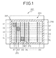
- FIG.1 is a general block diagram that shows a three-electrode surface discharge AC-driven plasma display panel and FIG.2 is a sectional view to illustrate the electrode structure of the plasma display panel shown in FIG.1.
- reference number 207 refers to a discharge cell (display cell)
- 210 refers to a rear glass substrate
- 211 and 221 refer to dielectric layers
- 212 refers to a phosphor
- 213 refers to a rib
- 214 refers to address electrodes (A1 to Ad)
- 220 refers to a front glass substrate
- reference number 222 refers to first electrodes (X electrodes: X1 to XL) or second electrodes (Y electrodes: Y1 to YL).
- Reference symbol Ca refers to capacitance between neighboring address electrodes
- Cg refers to capacitance between an address electrode and an opposite electrode (X electrode and Y electrode).
- a plasma display panel 201 is composed of two glass substrates, that is, the rear glass substrate 210 and the front glass substrate 220, and on the front glass substrate 220, the X electrodes (X1, X2, ..., XL) and the Y electrodes (scan electrodes: Y1, Y2, ..., YL) composed as sustain electrodes (including BUS electrodes and transparent electrodes) are arranged.
- the address electrodes (A1, A2, ..., Ad) 214 are arranged so as to be perpendicular to the sustain electrodes (Y electrodes and X electrodes), and each display cell 207, where discharge light emission is caused to occur by these electrodes, is formed in an area where two sustain electrodes, that is, an X electrode and the Y electrode, having the same number (Y1 and X1, Y2 and X2, and so on) that sandwich the area and an address electrode perpendicular to them, intersect.
- FIG.3 is a block diagram that shows the general configuration of a plasma display (PDP) apparatus that uses the plasma display panel shown in FIG.1, and also shows the main part of a drive circuit for the display panel.
- PDP plasma display
- a three-electrode surface discharge AC-driven plasma display apparatus comprises a display panel 201, a control circuit 205 that forms a control signal to control the drive circuit of the display panel by using an interface signal input from the outside, an X driver (X electrode drive circuit) 206 that drives panel electrodes by using the control signal from the control circuit 205, a scan electrode drive circuit (scan driver) 203 and a Y common driver 204, and an address electrode drive circuit (address driver) 202.
- the X common driver 206 generates sustain discharge (sustain) pulses and the Y common driver 204 also generates sustain pulses, and the scan driver 203 works so that the scan pulse is applied sequentially to each scan electrode (Y1 to YL).
- the address driver 202 applies an address voltage pulse corresponding to display data to each address electrode (A1 to Ad).
- the control circuit 205 comprises a display data control section 251 that receives a clock CLK and display data DATA and supplies an address control signal to the address driver 202, a scan driver control section 253 that receives a vertical synchronization signal Vsync and a horizontal synchronization signal Hsync and controls the scan driver, and a common driver control section 254 that controls the common drivers (the X common driver 206 and the Y common driver 204).
- the display data control section 251 comprises a frame memory 252.
- FIG.4 is a diagram that shows examples of the drive waveform of the PDP apparatus shown in FIG.3, and mainly shows general voltage waveforms to be applied to each electrode during an all-surface-write period (AW), an all-surface-erase period (AE), an address period (ADD) and a sustain period (sustain discharge period: SUS).
- AW all-surface-write period
- AE all-surface-erase period
- ADD address period
- SUS sustain period
- the drive periods that directly relate to image display are the address period ADD and the sustain period SUS, and it is designed so that image display is achieved at a fixed luminance by selecting pixels to be displayed during the address period ADD and causing the selected pixels to emit light during the subsequent sustain period.
- FIG.4 shows the drive waveforms in each subframe when a frame is composed of a plurality of subframes (subfields).
- a scan voltage pulse of -Vy level is sequentially applied instead.
- an address voltage pulse of +Va level is applied to each address electrode (A1 to Ad) and pixels on each scan line are selected.
- a sustain discharge (sustain) pulse of common +Vs level is applied alternately to all of the scan electrodes (Y1 to YL) and the X electrodes (X1 to XL) to cause sustain discharge to occur in the pixels selected previously, and display at a fixed luminance is achieved by means of the successive application.
- a sustain discharge (sustain) pulse of common +Vs level is applied alternately to all of the scan electrodes (Y1 to YL) and the X electrodes (X1 to XL) to cause sustain discharge to occur in the pixels selected previously, and display at a fixed luminance is achieved by means of the successive application.
- it will be possible to achieve a gradated display in density by combining basic actions of these drive waveforms to control the number of times of light emission.
- the all-surface-write period AW serves here to maintain the uniformity of the display characteristic by applying a write voltage pulse to all of the display cells in the panel to activate each display cell, and is inserted at certain periods.
- the all-surface-erase period AE serves to erase the previous display contents before addressing and sustaining for image display are initiated by applying an erase voltage pulse to all of the display cells.
- the sustain pulse is applied alternately to every X electrode and Y electrode and the address pulse is applied selectively to an electrode that corresponds to a lit- or unlit-cell.
- the address pulse has the same period as that of the scan pulse and the period is shorter than that of the sustain pulse.
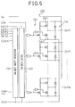
- FIG.5 is a block circuit diagram that shows an example of an IC used in the PDP apparatus shown in FIG.3.
- the drive IC to be connected to the address electrodes is assumed to have a 128-bit output
- 24 drive IC's are used in total.
- these 24 drive IC's are mounted in a plurality of modules so that each module is provided with a plurality of IC's.
- FIG.5 shows the internal circuit configuration of a drive IC chip equipped with the output circuits (234: OUT1 to OUT128) corresponding to 128 bits.
- Each output circuit 234 comprises a high voltage power supply wire V H and a ground wire GND connected to each other, with push-pull FET's 2341 and 2342 in the final output stage being sandwiched in between.
- a drive IC 230 further comprises logic circuits 233 to control both FET's, a shift register circuit 231 to select a 128-bit output circuit, and a latch circuit 232.
- control signals consist of a clock signal CLOCK of the shift register 231, data signals DATA1 to DATA4, a latch signal LATCH of the latch circuit 232, and a strobe signal STB for gate circuit control.
- the final output stage has a CMOS configuration (2341, 2342), but a totem pole configuration composed of MOSFET's of the same polarity can be applied.
- the drive IC chip is mounted on a rigid printed board and the pad terminals for the power supply, signal and output of the drive IC chip and the corresponding terminals on the printed board are connected by wire bonding.
- the output wire from the IC chip is connected to the end surface side of the printed board and an output terminal is provided, and the terminal is thermally compress-bonded to a flexible substrate that is provided with a similar terminal to form a module.
- a terminal for connection with a panel display electrode is provided and is used after being connected to the panel display electrode by techniques such as a thermal compression bonding or the like.
- each electrode described above is insulated from the circuit ground with respect to the direct current except for the dummy electrode in the panel end portion and, therefore, the capacitive impedance becomes dominant as the load in the drive circuit.
- a power recovery circuit is widely known, which makes use of the resonance phenomena to exchange energy between the capacitive load and an inductance.
- United States Patent No. 4,707,692 has disclosed a power recovery circuit in which the energy stored in a capacitor is applied again to a capacitive load by providing an inductor that makes up a resonant circuit together with the capacitive load and by performing on/off control of a switch at 1/4 period intervals of the resonance period in an electro-luminescent display apparatus.
- the energy is transferred between a capacitor 315 and loads 310/312.
- the energy in the capacitor is stored in the inductor and half of it charges the loads and the rest returns to the capacitor 315.
- the energy in the loads is once stored in the inductor and then is returned to the capacitor 315.
- United States Patent No. 5,081,400 and United States Patent No. 5,828,353 have disclosed a power recovery circuit that is switched at 1/2 period intervals of the sustain pulse when the sustain pulse is applied in the PDP apparatus.
- Japanese Unexamined Patent Publication (Kokai) No. 5-2449916 has disclosed a power recovery circuit used when an address pulse is applied from the address driver in the PDP apparatus.
- FIG.6 shows a low power drive circuit disclosed in Japanese Unexamined Patent Publication (Kokai) No. 2002-175044.
- power consumption is suppressed by driving a power supply terminal 121 of an address drive IC120 using a power recovery circuit 110 equipped with a resonance inductor 112.
- the power recovery circuit 110 outputs a normal constant address drive voltage at the timing of inducing address discharge to occur at an address electrode of a plasma display panel. Then the voltage of the power supply terminal 121 is lowered to the ground level before the switching states of an output circuit 122 in the address drive IC are switched.
- Japanese Unexamined Patent Publication (Kokai) No. 2002-175044 has also disclosed another technique to reduce power consumption for a capacitive load pulse drive circuit that is appropriate to be applied to an address driver and so on.
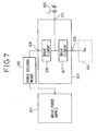
- FIG.7 is a diagram that shows an example of another capacitive load drive circuit disclosed in Japanese Unexamined Patent Publication (Kokai) No. 2002-175044. In this circuit, the power consumption in a drive device 306 in a drive circuit 303 is suppressed by dividing it to a power dividing means 330 composed of resistors, a constant current circuit, and so on.
- Japanese Unexamined Patent Publication (Kokai) No. 9-62226 has disclosed a configuration that is used to recover the energy discharged from the X electrode to charge the Y electrode, and to recover the energy discharged from the Y electrode to discharge the X electrode, when sustain pulses are applied alternately to the X electrode and Y electrode.
- the drive circuit disclosed in United States Patent No. 4,707,692, United States Patent No. 5,081,400, United States Patent No. 5,828,353, Japanese Unexamined Patent Publication (Kokai) No. 5-249916, Japanese Unexamined Patent Publication (Kokai) No. 9-62226, and shown in FIG.6 is one that reduces the power consumption by utilizing the resonance phenomenon, but there is a problem that the power consumption suppressing effect is considerably lessened as the definition of the plasma display panel becomes higher and the size of its screen becomes larger.
- the sustain pulse is applied to all of the sustain electrodes and the capacitive load is constant.
- the address pulse is applied to each load electrode independently of each other according to the display video, the load capacitance to be driven changes considerably.
- the configuration disclosed in Japanese Unexamined Patent Publication (Kokai) No. 5-2449916 can be used to reduce the power consumption, but when the same image continues in the vertical direction and the state of each load capacitance does not change, a problem occurs that the power consumption becomes large if the configuration disclosed in Japanese Unexamined Patent Publication (Kokai) No. 5-2449916 is used.
- the capacitive load drive circuit that uses the power dividing method shown in FIG.7, it is also possible to suppress heat generation in all the system, including the power supply circuit, and further reduce the cost, if the input power from the drive power supply 301 to the drive circuit 303 can be further decreased.
- the power consumption in the drive circuit 303 cannot be suppressed sufficiently, the cost relating to heat dissipation in each part of the display and the cost of parts are raised. Moreover, there is possibility that the light emission luminance is suppressed by the limit of heat dissipation of the display apparatus itself, or the characteristic of the flat panel display of being able to be made thinner and lighter is not utilized fully.
- a capacitive load drive circuit able to not only suppress the power consumption (heat generation) but also suppress the increase in cost of each part of the display even when the drive circuit is sped up, and to provide a display apparatus such as a PDP apparatus using the same.
- a capacitive load drive power supply circuit characterized by the use of a transformer.
- each one end of the primary coil and the secondary coil of a transformer is connected to an output terminal to be connected to a capacitive load
- a first switch circuit is connected between the other end of the primary coil and a first reference potential
- a second switch circuit is connected between the other end of the secondary coil and a second reference potential
- a power supply switch circuit is connected between the output terminal and a drive power supply.
- the power consumption in the drive circuit can be minimized by properly selecting a circuit section (drive load) into which the electromagnetic energy is to be directed for reuse, and by properly designing the exciting inductance of the secondary coil.
- the energy loss during the energy re-entry is compensated for by the drive power supply via the power supply switch circuit.
- a third switch circuit composed of a one-way conductive element is further provided between the output terminal and the first reference potential.
- the second switch circuit can be composed of the one-way conductive element.
- connection point of the primary coil and the first switch circuit and a fifth reference potential
- the fifth reference potential is, for example, an output terminal of the drive power supply
- the fourth switch circuit can be composed of the one-way conductive element.
- the power consumption can be divided.
- a capacitive load drive power supply circuit is characterized in that it uses an inductance element but not a capacitor.
- a first switch circuit, a coil and a second switch circuit are connected in series between the output terminal to be connected to a capacitive load and a first reference potential, a third switch circuit is connected between the connection point of the first switch circuit and the coil, and the first reference potential, a fourth switch circuit is connected between the connection point of the coil and the second switch circuit, and the output terminal, and the power supply switch circuit is connected between the output terminal and the drive power supply.
- resonance is caused to occur between the capacitance of the drive load and the exciting inductance of the coil by connecting the drive load to the first reference potential via the coil and the first and second switch circuits.
- the energy loss during the process of reusing the above-mentioned energy is compensated for from the drive power supply via the power supply switch circuit.
- the third switch circuit and the fourth switch circuit can be composed of the one-way conductive elements.
- an impedance circuit is connected to the path to which the power supply switch circuit is connected.
- the capacitive load drive power supply circuit described above is proper for use as a power supply circuit for a capacitive load drive circuit such as an address driver in a PDP apparatus.
- a capacitive load drive circuit comprises a capacitive load, a first drive power supply, a second drive power supply, and first and second drive elements that are connected in series between the first drive power supply and the second drive power supply and, the connection point of which is connected to the capacitive load, and the capacitive load drive power supply circuit described above is used for either of the first or the second drive power supply.
- an address driver in a PDP apparatus there are a plurality of capacitive loads and a plurality of pairs of first and second drive elements for driving the plurality of capacitive loads, respectively, but first and second drive power supplies are connected commonly to the plurality of pairs of the first and second drive elements.
- the plurality of capacitive loads are set to the individual potential states independent of each another but, when the potential state is set, all the plurality of capacitive loads are connected to the capacitive load drive power supply circuit and the stored electrostatic energy is once recovered to the capacitive load drive power supply circuit to be stored as electromagnetic energy, and then all of the drive elements are changed to the first potential.
- one of the first and second drive elements is brought into a conductive state, and the output terminal of the drive power supply is changed to the second potential by discharging the electromagnetic energy stored in the capacitive load drive power supply circuit, and the corresponding capacitive load is changed to the second potential through the first or second drive element.
- the power consumption increases when the number of load capacitances that change for each display line is large, and the power consumption can be reduced by performing the above-mentioned power recovery function of the capacitive load drive power supply circuit, but when the state of each load capacitance does not change, the power consumption is small and the power consumption can be reduced, on the contrary, by not performing the power recovery function.
- a current detection circuit that detects the current flowing out from the drive power supply is provided to the path to which the power supply switch circuit of the capacitive load drive power supply circuit is connected, and whether the power recovery function of the capacitive load drive power supply circuit is performed is controlled in accordance with the detection result.
- an expected value of the power consumption in the drive circuit is calculated from the information about the changes in each drive state of the plurality of capacitive loads and whether the power recovery function of the capacitive load drive power supply circuit is performed is controlled.
- a temperature detection circuit that detects the temperature of a part of the capacitive load drive circuit such as an address driver and whether the power recovery function of the capacitive load drive power supply circuit is performed is controlled in accordance with the detected temperature.
- the energy used to release the sustain pulse applied to the X electrode in a PDP apparatus is recovered and is reused to apply the sustain pulse to the Y electrode immediately after, and moreover, the energy used to release the sustain pulse applied to the Y electrode is recovered and is reused to apply the sustain pulse to the X electrode immediately after, and this cycle is repeated.
- the energy of the sustain pulse to be applied to both X electrode and Y electrode is recovered by the X common drive circuit and the Y common drive circuit and is once stored in the capacitor, then the energy of the sustain pulse recovered from the X electrode to the capacitor is reused to apply the sustain pulse to the X electrode next time, and the energy of the sustain pulse recovered from the Y electrode is reused to apply the sustain pulse to the Y electrode next time.
- 9-62226 has disclosed a configuration in which the power recovery circuit is provided between the X common drive circuit and the Y common drive circuit, and the energy of the sustain pulse applied to the X electrode is recovered and once stored in the capacitor and the energy thus stored in the capacitor is used for the application of the sustain pulse to be applied to the Y electrode immediately after, and similarly the energy of the sustain pulse applied to the Y electrode is recovered and once stored in the capacitor and the energy thus stored in the capacitor is used for the application of the sustain pulse to be applied to the X electrode immediately after.
- the recovered energy is once stored in the capacitor in either case, and then the energy stored in the capacitor is taken out and used for application of the sustain pulse.
- a capacitor to which energy is temporarily stored is not used but only an inductance element (coil circuit) is used, and the energy used when the voltage applied to one of two electrodes forming the drive load is released is recovered and is reused to apply a voltage to the other electrode immediately after.
- the recovery efficiency is no longer dependent on the period of the sustain pulse and a sustain pulse of a high frequency can be handled.
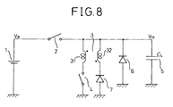
- FIG.8 shows the configuration of the display drive circuit in the first embodiment of the present invention.
- reference number 5 denotes a capacitive load that represents the drive terminal of a display.
- the capacitance of the drive load is assumed to be C L , and the applied voltage, V H .
- a drive power supply 1 supplies a voltage Va to the drive load.
- V H to the drive load 5 is raised or lowered, a power supply switch circuit 2 is once brought into the OFF-state (open state).
- a first switch circuit 4 When the applied voltage is lowered, a first switch circuit 4 is brought into the ON-state (conductive state), and the electrostatic energy stored in C L is converted into the electromagnetic energy in a primary coil 31 by causing resonance to occur between the load capacitance C L and the primary coil 31 of a transformer 3.
- a secondary coil 32 As a secondary coil 32 is wound in the direction shown schematically, during resonance, an electromotive force is produced in the direction such that the cathode side of a diode 7 is high potential. Due to this, the diode 7 is shut off and no current flows through the secondary coil 32, the resonance is under the control of the characteristic of the primary coil.
- the applied voltage V H drops to 0V, and a diode 6 is brought into conduction and the voltage between the terminals of the primary coil becomes nearly equal to 0V. If the voltage V H drops to 0V, the diode 6 is not necessary. At this time, almost all the electrostatic energy stored in C L is converted into the electromagnetic energy of the primary coil 31.
- the switch circuit 4 is switched to the OFF-state from this state, the current in the primary coil 31 decreases in magnitude, and at the same time, because an electromotive force is induced in the secondary coil 32 in the direction such that the diode 7 is brought into conduction, the stored electromagnetic energy is discharged from the secondary coil 32.
- the applied voltage V H is raised.
- the energy loss due to the connection loss of resistive components and transformers in each part of the circuit is compensated for, from the drive power supply 1, by switching the switch circuit 2 into the ON-state.
- the primary coil 31 of the transformer 31 and the switch circuit 4 change their connected positions.
- the diodes 6 and 7 with switch elements controlled from the outside, respectively, such as a MOSFET and IGBT. In this case, it is also possible to change the positional relation between the secondary coil 32 and the switch element corresponding to the diode 7.
- the present invention can be applied to an electro-luminescent display, a liquid crystal display, or a CRT display, in addition to a plasma display, as long as the drive load can be regarded as a capacitive load.
- the load capacitance C L When the load capacitance C L is recharged, it cannot be charged to a voltage Va only by the resonance energy because of the loss of resonance energy, therefore, the switch circuit 2 is brought into conduction immediately before or after the completion of recharging so that it is charged to the voltage Va.
- FIG.9 is a diagram that shows the general configuration of the PDP apparatus in the second embodiment of the present invention
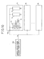
- FIG.10 is a diagram that shows the power supply of an address driver.
- the PDP apparatus in the second embodiment differs from the conventional PDP apparatus in that an address driver power recovery power supply 260 is provided.
- the power supply of the address driver 202 is one that supplies only voltage Va and ground GND.
- the PDP apparatus in the second embodiment once recovers and reuses the power retained by the address electrode, when the address driver power recovery power supply 260 supplies the voltage Va to the high-potential power terminal of the address driver 202.
- the address electrodes in the plasma display panel are drive loads 51 each having a capacitance C L , and drive IC's 70, 75 and 76 that drive these are mounted in drive modules 77 to 79 in plural units to improve their mountability and heat radiating performance.
- the address driver power recovery power supply 260 supplies the voltage Va that is applied commonly to the drive IC's within these drive modules.
- V H denotes the voltage at a terminal 700.
- the ground voltage GND to be applied commonly to the drive IC's in the drive modules is supplied similarly as before. Due to this, the power consumption of all the drive IC's can be reduced.
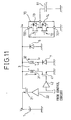
- FIG.11 is a diagram that shows the configuration of the address driver power recovery power supply 260 in the second embodiment, and only a pair of drive devices of the drive IC 70 are shown here.
- the address driver power recovery power supply 260 in the second embodiment is composed of the capacitive load drive circuit in the first embodiment.
- the drive IC 70 directly drives the drive load 51 and the voltage Va is supplied to the high-potential power terminal 700 of the drive IC 70 from the address driver power supply recovery power supply 260.
- a high-side MOSFET 71 and a low-side MOSFET 72 are integrated and these MOSFET's are parasitized by diodes 73 and 74, respectively.
- MOSFET's 21 and 41 are used as the switch circuits 2 and 4, respectively, in the first embodiment shown in FIG.8, and these MOSFET's are driven by buffer circuits 22 and 42, and the control signal is supplied from the control circuit 205.
- MOSFET's and diodes are used here in each switch circuit, but it is needless to say that these can be replaced with proper semiconductor devices or switch devices such as IGBT's and bipolar transistors.
- the transformer 3 an air-core transformer, the coupling coefficient of which has been improved by techniques such as the bifilar winding, the sandwich winding, and the space winding, can be applied.
- a transformer can be used, the coupling coefficient of which has been improved, the characteristic of which has been stabilized, and the size of which has been reduced, by using general core materials such as a ferrite and a dielectric material.
- the winding can be a single wire, but a stranded wire or a parallel winding or a series winding are recommended, if the skin effect or the proximity effect is aimed at within the limit of the transformer in size and cost.
- FIG.12 the power supply terminal voltage V H of the drive IC, the states of the MOSFET's 21 and 41, the current I 1 of the primary coil and the current I 2 of the secondary coil of the transformer 3, and the state of the drive IC 70 are shown in this order from top to bottom as time elapses.
- the conventional power supply circuit when the output state of the drive IC 70 switched from output (L n ) to output (L n+1 ), a part or the whole of the transferred energy accompanying the raise and drop of the voltage of the drive load 51 is consumed by internal devices 71 and 72 within the IC.
- the electrostatic energy stored in the drive load 51 is taken out from the power supply terminal 700 of the drive IC 70 to the primary coil 31 of the transformer 3.
- the MOSFET 41 is turned ON.
- the current I 1 in the primary coil 31 increases to Va (C L / L 1 ) 1/2 in a sinusoidal manner.
- the time T1 is ⁇ (C L / L 1 ) 1/2 as shown in the mathematical expression 2, that is, it is halved compared to the conventional drive method shown in FIG.6, therefore, a high-speed drive can be realized.
- T 1 ⁇ L 1 C L / 2
- T 2 ⁇ L 2 C L / 2
- T 3 ⁇ L 3 C L / 2
- the diode 6 For reduction in cost, it is also possible to eliminate the diode 6 and utilize the conductive states of the parasitic diodes 73 and 74 within the drive IC 70.
- the diode 6 when the diode 6 is eliminated, there may be a case where the decrease in the current I 1 , denoted by the alternating long and short dashed line a in the waveform of I 1 , cannot be ignored. Therefore, when the conduction period of the MOSFET 41 is extended, the energy loss should be taken into consideration. Then, after the output state of the drive IC 70 switches to output (L n+1 ), the MOSFET 41 is turned OFF.
- the MOSFET 41 can be turned OFF.
- the maximum value of the current I 2 is the maximum value (L 1 / L 2 ) 1/2 of the current I 1 , but it decreases as the coupling coefficient between the primary and secondary coils decreases.
- the resonance time T 2 of the secondary coil is ⁇ (L 2 / C L ) 1/2 as shown in the mathematical expression 1, that is, it is halved compared to the conventional method.
- the diode 6 is connected to the ground but it can be connected to a potential point other than the ground potential in order to, for example, speed up the power reproduction in the drive load 5 or reduce the power supplied from the drive power supply 1.
- the solid lines denote the waveforms of V H and I 2 when L 1 and L 2 are designed so as to be equal to each other.
- the conductive resistance of the parasitic diode 73 is the factor of the power loss.
- the ON-state resistance of the high-side MOSFET 71 is the conductive resistance of which is generally higher than that of the parasitic diode 73, is the factor of the power loss. Because of these power losses, the electrostatic energy to be reproduced in the load capacitance decreases and, therefore, the power supply terminal voltage V H after the resonance time T 2 becomes lower than the drive power supply voltage Va.
- the power loss is compensated for from the drive power supply 1 by bringing the MOSFET 21 into the ON-state after the resonance time T 2 elapses.
- the power loss caused by the resistance described above can be reduced. If the drive voltage of the load capacitance is constant, the average current corresponding to the amount of charge for charging is also constant, but the effective value of the current becomes smaller for the lower peak values of the current, because it is in proportion to the average value of the current squared.
- the resonance time also increases, but it is possible to reduce the peak value of the resonance current and the effective value.
- the reproduced energy in the load capacitance increases as shown by the broken line waveform of the power supply terminal voltage V H .
- priority is given to a high-speed drive, it is possible to bring the MOSFET 21 into the ON-state earlier during resonance as shown by the solid line.
- the power loss can be reduced compared to the case where the L 1 is equal to L 2 .
- the inductance L 2 can be made smaller than the inductance L 1 .
- the power supply having the power recovery function is used as the power supply on the high-potential side of the drive IC in the second embodiment, it is also possible to provide the power supply on the low-potential side with the power recovery function.
- the high-potential power terminal 700 of the drive IC 70 is connected to the ground potential
- the low-potential power terminal 701 is connected to the output terminal of the address driver power recovery power supply described above, not to the ground point.
- the drive power supply 1 and the semiconductor devices such as the MOSFET's 21 and 41, and the diodes 6 and 7 in the circuit of the address driver power recovery power supply reverse their polarity.
- level shift has to be performed on the control signal via circuits such as the photocoupler circuit or the condenser coupling circuit when the drive IC 70 is a type that inputs the control signal with respect to the reference of the potential of the low-potential power terminal 701 and the control signal is input with respect to the reference of the ground potential.
- the voltage between Va/2 and - Va/2 is applied to the drive load 51, it is possible to connect the address driver power recovery power supply equipped with the drive power supply 1 that gives the reference potential of Va/2 to the high-potential power terminal 700 of the drive IC 70, and connect the potential reference point of - Va/2 to the low-potential power terminal 701.
- FIG.13 is a diagram that shows the configuration of the address driver power recovery power supply in the PDP apparatus in the third embodiment of the present invention.
- the address driver power recovery power supply in the third embodiment differs from the power supply in the second embodiment in that the connection point between the primary coil 31 and the first switch circuit 41 is connected to the terminal of the power supply 1 via a diode 43.
- the gate of the N-channel MOSFET 23 is driven by a buffer circuit 23 with respect to the reference of the source potential.
- An integrated circuit driven by a floating power supply capacitor connected to the source potential of the MOSFET 23 can be used instead of the buffer circuit 24.
- a pulse transformer connected between the source and the drain of the MOSFET 23 can also be used. Moreover, it is possible to suppress the counter-electromotive force produced in the primary coil 31 by connecting the cathode terminal of the diode 43 to another potential point and not to the drive power supply 1.
- a constant current source switch circuit is used as the switch circuit 2 shown in FIG.8. If the switch circuit 2 is operated as a constant current source in the ON-state, it is possible to suppress the effective value of the drive current that flows through the drive IC and the power consumption to a low level. In concrete terms, current feedback is performed on the drive device used in the switch circuit.
- a feedback resistor 25 is connected in series to the source of the MOSFET 23 shown in FIG.13 and the drive voltage from the buffer circuit 24 is applied between the feedback resistor 25 and the gate of the MOSFET 23.
- the circuit shown in FIG.8 it is also possible to obtain an operation equivalent to that of the constant current source obtained from the above-mentioned MOSFET 23 and the resistor 25, because the conductive impedance of the switch circuit 2 in the ON-state is raised by inserting impedances (circuits) such as a resistor and a constant current circuit in series with the switch circuit 2.
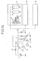
- FIG.14 is a diagram that shows the configuration of the address driver power recovery power supply in the PDP apparatus in the fourth embodiment of the present invention.
- the display drive circuit in the fourth embodiment differs from that in the third embodiment in that the secondary coil 32 of the transformer 3 is connected to the source terminal of the MOSFET 23 that operates as a constant current source while it is in the ON-state. Due to this, the drive current toward the drive modules 77 to 79 including the drive IC70 is always made to be a constant current at the rise of the applied voltage V H , and the effective value is minimized.
- the charges to be supplied from the drive power supply 1 are reduced by the amount corresponding to the amount of charges supplied from the secondary coil 32, and the power consumption of the whole of the drive circuit can be reduced. Therefore, even in a case where a large load capacitance such as that when a matrix electrode of the plasma display panel is driven, the cost for heat dissipation of the drive module 77, and so on, can be suppressed.
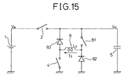
- FIG.15 is a diagram that shows the configuration of the capacitive load drive circuit in the fifth embodiment of the present invention.
- a low power circuit equivalent to the drive circuit shown in FIG.8 can be realized by using an inexpensive coil 8 instead of a transformer.
- the capacitive load drive circuit in the fifth embodiment is also suitable for use as a power supply of an address driver in a PDP apparatus.
- FIG.16 the applied voltage V H to the drive load 5, the states of the switch circuits 2 and 4 and a switch circuit 81, and the current I 3 of the coil 8 are shown in this order from top to bottom.
- the output state of the drive IC 70 when the drive load 5 is driven via the drive IC 70 is also shown in brackets.
- the electrostatic energy stored in the drive load 5 is taken out into the coil 8 to reduce the power consumption by bringing the switch circuits 81 and 4 into the ON-state. For this purpose, first the switch circuit 81 is brought into the ON-state and after the switch circuit is brought into the OFF-state, the switch circuit 4 is brought into the ON-state.
- the current I 3 of the coil 8 increases up to Va (C L / L 3 ) 1/2 in a sinusoidal manner.
- the time T 3 is ⁇ (L 3 ⁇ C L ) 1/2 , as shown in the mathematical expression 1, that is, a half of that in the conventional drive method shown in FIG.6 and therefore a high-speed drive can be realized.
- the drive IC 70 the current is taken out from the power supply terminal 700 via the parasitic diode 73 of the high-side MOSFET 71, therefore, it is possible to switch the states of the high-side MOSFET 71 and the low-side MOSFET 72 to speed up the circuit operation only by prohibiting the low-side MOSFET 72 from changing from the OFF-state to the ON-state.
- the MOSFET 41 can be brought into the OFF-state only if the ON-state of the high-side MOSFET 71 within the drive IC 70 is maintained.
- the very instant that the current I 3 is about to decrease because the switch circuit 4 is brought into the OFF-state a counter-electromotive force is produced in the direction that brings a diode 83 into conduction and the current I 3 decreases while describing a sinusoidal resonance waveform as shown schematically.
- the resonance time T 3 is slightly longer or shorter, depending on the resistance in the path of the resonance current. Then, the switch circuit 2 is brought into the ON-state to supply the drive voltage Va to the drive load and the switch circuit 81 is brought into the ON-state in preparation for the subsequent repetitious operation.
- FIG.17 is a diagram that shows the configuration of the address driver power recovery power supply in the sixth embodiment of the present invention.
- Each of the address driver power recovery power supplies in the first to the fourth embodiments described above can reduce the power consumption significantly when handling a display signal for a display pattern that changes considerably.
- the power consumption can be suppressed sufficiently even by the conventional method, and, if the above-mentioned embodiments are applied without any changes made to them, a drive pulse of high frequency is applied forcedly to the drive load 51 as a result, and the power consumption in the drive circuit increases, on the contrary, compared to the case of the conventional method.
- a detection circuit 15 for the power supply current is inserted in series between the drive power supply 1 and the switch circuit 2, and the output terminal of the current detection circuit 15 is connected to the input terminal of a drive control circuit 18. Then, for a display that only consumes power considerably in the drive circuit, the power recovery function is activated as before.
- the power supply current flowing out of the drive power supply 1 is detected using the current detection circuit 15, the detected output is input to the control circuit 18, and the switch circuit 4 is activated when the current value exceeds a certain value.
- the current detection circuit 15 can be inserted to any position such as between the switch circuit 2 and the output terminal as long as the power supply current flowing out of the drive power supply 1 can be detected.
- FIG.18 is a diagram that shows an example of the configuration of the current detection circuit.
- the current detection circuit 15 is composed of a current detection resistor 16 and a detected voltage conversion circuit 17.
- the power supply current of the drive power supply 1 can be detected by the voltage drop across the current detection resistor 16 caused in proportion to the power supply current.
- the detected voltage conversion circuit 17 converts the detected voltage into a signal (voltage, current, pulse, etc.) that can be easily handled in the drive control circuit 18, and outputs it to the drive control circuit 18.
- the detected voltage conversion circuit 17 can detect the above-mentioned voltage drop only from the terminal that is not connected to the drive power supply 1 of the current detection resistor 16, with respect to the reference of the ground potential. Or, it can detect accurately from both terminals of the current detection resistor 16 even when the detected voltage is small, if the connection denoted by the broken line is added.
- FIG.19 is a diagram that shows the address driver power recovery power supply in the PDP apparatus in the seventh embodiment of the present invention, in which, similar to the sixth embodiment, the power supply current flowing out of the drive power supply 1 is detected and the switch circuit 4 is activated when the current valued exceeds a certain value in the PDP apparatus, in which the capacitive load drive circuit in the fifth embodiment shown in FIG.15 is applied to the address driver power recovery power supply.
- the current detection circuit 15 is provided between the switch circuit 2 and the output terminal.
- FIG.20 is a diagram that shows the configuration of the PDP apparatus in the eighth embodiment of the present invention.
- the power supply current flowing out from the drive power supply 1 is detected in the sixth and seventh embodiments, the power consumption in the drive circuit can be estimated also by detecting the display signal in the PDP apparatus.
- the display data control section 251 in the control circuit 205 is provided with a load variation detection circuit 261 and the power recovery operation by the address driver power recovery power supply 260 is controlled on the basis of the detected result.
- the address driver power recovery power supply 260 is, for example, one of the circuits shown in the second to seventh embodiments.
- the load variation detection section 261 estimates the power consumption of the drive circuit from the input clock signal and the display data signal.
- the load variation can be obtained by counting the number of output pulses of the individual address driver IC or the address drive module obtained from the clock signal and the display data signal.
- the power consumption in the drive circuit also increase or decreases.
- the power consumption in the drive circuit is obtained by assigning weights of the following kind to the number of pulses, with the parasitic capacitance between neighboring output lines being taken into consideration. In other words, in accordance with the switching relation of the outputs between the neighboring output terminals and the output terminal that is the target of calculation, a heavier weight is assigned according to the following priority.
- FIG.21 a diagram that shows the configuration of the drive system of the address driver in the PDP apparatus in the ninth embodiment of the present invention, which is a case where the capacitive load drive circuit in the fifth embodiment is applied to the address driver power recovery power supply.
- the circuit power consumption is reduced when a display pattern that requires a large circuit power consumption is displayed by activating the recovery operation of the address driver power recovery power supply when the detected temperature exceeds a certain value, and when the circuit power consumption is small, on the contrary, the circuit power consumption is prevented from increasing, without the recovery operation.
- the address drive IC 70 is provided with a temperature detector 58 such as a thermistor, and a temperature detection control circuit 59 detects the temperature from the detected signal of the temperature detector 58 and controls the operation of the switch circuit 4.
- a temperature detector 58 such as a thermistor
- a temperature detection control circuit 59 detects the temperature from the detected signal of the temperature detector 58 and controls the operation of the switch circuit 4.
- the switch circuit 4 is prevented from operating by shutting off the control signal thereto.
- the address drive IC 70 is provided with the temperature detector 58 such as a thermistor in the ninth embodiment, it is also possible to detect the temperature of a power consuming device directly or indirectly by mounting a temperature detector on the address drive module 77, a heat radiating board used for it, or a wiring member such as a flexible substrate provided on the heat radiating board, or by attaching it to a power consuming device or to its periphery by screwing or bonding.
- an IC for detecting temperature or the like can be used.
- the power consumption reducing function according to an embodiment of the present invention is activated immediately when the power consumed or the temperature detected in the drive circuit described above exceeds a certain threshold, and the operation is terminated when the power consumption or the temperature falls below the threshold.
- this method minimizes the size of the control program, there is possibility that switching noises may be discerned by the operator, which are produced when the power consumption reducing function is activated and terminated repeatedly each time the display pattern changes. To avoid this, therefore, there is another method in which the power consumption reducing function is activated or terminated a certain period after the threshold is exceeded or the value falls below the threshold.
- the power consumption operation is provided with a hysteresis characteristic by setting two thresholds.
- the power consumption reducing function according to an embodiment of the present invention is performed when the power consumed or the temperature detected in the drive circuit described above exceeds a first threshold and the power consumption reducing operation is terminated when the power consumption or the detected temperature falls below a second threshold, which is lower than the first threshold. Due to this hysteresis characteristic, the possibility that the noises are recognized is reduced because the power consumption reducing operations may be switched in synchronization with the change of images.
- control over activation and termination of the power consumption reducing function on the basis of the power consumption of the drive circuit or the detected temperature of the device, as described above, can also be applied to the previously-proposed drive circuit, the power consumption of which has been reduced, disclosed in Japanese Unexamined Patent Publication (Kokai) No. 5-249916 shown in FIG.6 or in Japanese Patent Application No. 2000-301015 shown in FIG.7.
- FIG.22 is a diagram that shows the configuration of the part of the panel 201, the X common driver, the scan driver 203 and the Y common driver in the PDP apparatus in the tenth embodiment of the present invention.
- the sustain electrode drive circuit (X common driver and Y common driver (common driver, together)) in the plasma display panel 201 drives a capacitive load, the load capacitance of which can be regarded as constant.
- a common drive voltage V Y is applied to the Y electrodes Y1 to YL of the plasma display panel 201, shown in FIG.22, via the drive module 203 on which the scan drive IC is mounted, and a common drive voltage V X is also applied to the X electrodes X1 to XL during the sustain period, as shown in FIG.4.
- V X is also applied to the X electrodes X1 to XL during the sustain period, as shown in FIG.4.
- there can be a method for widening the margin to absorb the panel dependency of the drive voltage and for increasing the luminance of the display in which the period during which the voltage being applied to the X electrodes and Y electrodes is 0V in the sustain period shown in FIG.4 is shortened and the drive duty is increased.
- FIG.24 is a diagram that shows the configuration of the part of the panel 201, the X common driver, the scan driver 203 and the Y common driver in the PDP apparatus in the eleventh embodiment.
- drive circuit in the tenth embodiment it is possible to further reduce the power consumption and the cost of the drive circuit, the load capacitance of which can be regarded as constant, as similar to the common driver in the plasma display panel 201.
- the common drive voltage V Y is applied to the Y electrodes Y1 to YL of the plasma display panel 201 shown in FIG.24 via the drive module 203 on which the scan drive IC is mounted and, also, the common drive voltage V X is applied to the X electrodes X1 to XL.
- the power consumption in the drive circuit is almost proportional to the second power of the drive voltage and the drive frequency. Therefore, if ⁇ Va is applied, as is conventionally done, between the X and Y electrodes of the plasma display panel 201 while the amplitude of the drive pulse of V X and V Y is being kept at Va/2, that is, a half of the conventional one, as shown in the waveform diagram in FIG.25, the power consumption in the drive circuit can be halved. In this case, even if the pulse frequency is doubled, the consumed energy per pulse period becomes 1/4.
- V X falls below the minimum potential of the pulse waveform, a diode 61 is brought into conduction and V X is kept almost at the minimum potential.
- a parasitic diode in an element making up a switch circuit 97 or a diode newly loaded in parallel can be used instead of the diode 61. Then, when the switch circuit 63 is brought into the OFF-state, the current flowing through the coil 311 is shut off and the electromagnetic energy in the transformer 3 flows into the Y electrode of the plasma display panel 201 via the other coil 321 and a diode 66.
- the power consumption in the drive circuit can be reduced by efficiently converting and reproducing the electromagnetic energy stored in the transformer 3 into the electrostatic energy of the capacitance of the Y electrode, via the resonance between the coil 321 and the capacitance of the Y electrode.
- the same operation is performed repeatedly when lowering the voltages V X and V Y of the X and Y electrodes by switching floating switch circuits 99 and 100. (There are four patterns, because each electrode voltage is lowered from VA/2 and 0V, respectively.)
- the present embodiment it is possible to use inexpensive drive devices, diodes, and transformers, the withstand voltage of which have been halved, in each switch circuit or as circuitry parts.
- the drive voltage, the amplitude of which is halved is applied differentially between the X electrode and the Y electrode of the plasma display panel 201 in the description of the present embodiment, it is needless to say that the drive voltage can be applied between terminals of the same X electrode or between an odd-numbered terminal and an even-numbered one of the Y electrodes. Therefore, by using the present embodiment, it is possible to realize a fast low-power consumption drive circuit able to wide the margin of the drive voltage or to increase the luminance of a display by increasing the pulse frequency while suppressing the power consumption and the cost of the drive circuit significantly.
- each embodiment can be applied to a plasma display panel, a liquid crystal panel, an electro-luminescent panel, a field emission display (FED) panel, and so on, which have a matrix electrode and which can be regarded as a capacitive load, in addition to the plasma display panel that is the target to be driven.
- FED field emission display
- Braun tubes or fluorescent tubes (those used as a backlight of a liquid crystal display are also included), the drive load of which shows a capacitive impedance, are included as the drive load in embodiments of the present invention.
- the present invention it is possible to suppress the power consumption (heat generation) in a drive circuit that drives a display device at high speed, and at the same time to suppress an increase in the circuitry cost.
- SVGA 800 x 600 dots
- SXGA (1280 x 1024 dots a high luminance plasma television with a high gradation
- TV and HDTV high gradation
Landscapes
- Engineering & Computer Science (AREA)
- Physics & Mathematics (AREA)
- Power Engineering (AREA)
- Plasma & Fusion (AREA)
- Computer Hardware Design (AREA)
- General Physics & Mathematics (AREA)
- Theoretical Computer Science (AREA)
- Control Of Indicators Other Than Cathode Ray Tubes (AREA)
- Control Of Gas Discharge Display Tubes (AREA)
- Transforming Electric Information Into Light Information (AREA)
Applications Claiming Priority (2)
| Application Number | Priority Date | Filing Date | Title |
|---|---|---|---|
| JP2002346165A JP2004177815A (ja) | 2002-11-28 | 2002-11-28 | 容量性負荷駆動回収回路、容量性負荷駆動回路及びそれを用いたプラズマディスプレイ装置 |
| JP2002346165 | 2002-11-28 |
Publications (2)
| Publication Number | Publication Date |
|---|---|
| EP1424678A2 true EP1424678A2 (fr) | 2004-06-02 |
| EP1424678A3 EP1424678A3 (fr) | 2007-08-22 |
Family
ID=32290475
Family Applications (1)
| Application Number | Title | Priority Date | Filing Date |
|---|---|---|---|
| EP03255475A Withdrawn EP1424678A3 (fr) | 2002-11-28 | 2003-09-02 | Circuit d'attaque pour charge capacitive et appareil d' affichage à plasma utilisant ce type de circuit |
Country Status (6)
| Country | Link |
|---|---|
| US (1) | US20040104866A1 (fr) |
| EP (1) | EP1424678A3 (fr) |
| JP (1) | JP2004177815A (fr) |
| KR (1) | KR20040047558A (fr) |
| CN (1) | CN1504979A (fr) |
| TW (1) | TWI241547B (fr) |
Cited By (3)
| Publication number | Priority date | Publication date | Assignee | Title |
|---|---|---|---|---|
| CN100407251C (zh) * | 2004-09-07 | 2008-07-30 | Lg电子株式会社 | 等离子显示设备及其驱动方法 |
| WO2010088954A1 (fr) * | 2009-02-04 | 2010-08-12 | Osram Gesellschaft mit beschränkter Haftung | Circuiterie et procédé pour faire fonctionner une feuille électroluminescente |
| US11860101B2 (en) | 2020-04-17 | 2024-01-02 | Korea Advanced Institute Of Science And Technology | Multi-photon microscopy and imaging method, lowering repetition rate to use time-gated detection |
Families Citing this family (25)
| Publication number | Priority date | Publication date | Assignee | Title |
|---|---|---|---|---|
| KR100550983B1 (ko) * | 2003-11-26 | 2006-02-13 | 삼성에스디아이 주식회사 | 플라즈마 표시 장치 및 플라즈마 표시 패널의 구동 방법 |
| KR20050090863A (ko) * | 2004-03-10 | 2005-09-14 | 삼성에스디아이 주식회사 | 플라즈마 표시 패널 및 그의 erc 타이밍 제어 방법 |
| US20050219165A1 (en) * | 2004-03-31 | 2005-10-06 | Paul Regen | Electroluminescent color-change technology |
| JP4532244B2 (ja) * | 2004-11-19 | 2010-08-25 | 日立プラズマディスプレイ株式会社 | プラズマディスプレイ装置 |
| KR100588019B1 (ko) * | 2004-12-31 | 2006-06-12 | 엘지전자 주식회사 | 플라즈마 디스플레이 패널의 에너지 회수장치 및 방법 |
| KR100908714B1 (ko) | 2005-01-17 | 2009-07-22 | 삼성에스디아이 주식회사 | 플라즈마 표시 장치 및 그 구동 방법 |
| CN100412924C (zh) * | 2005-06-09 | 2008-08-20 | 乐金电子(南京)等离子有限公司 | 等离子显示模块的变压器控制装置及方法 |
| TWI345755B (en) * | 2005-06-21 | 2011-07-21 | Chunghwa Picture Tubes Ltd | Method of switching a high-side switch of a pdp scan circuit in a zero-voltage-switching mode |
| TWI349917B (en) * | 2005-06-22 | 2011-10-01 | Chunghwa Picture Tubes Ltd | Multi-mode switch for plasma display panel |
| CN1885696A (zh) * | 2005-06-22 | 2006-12-27 | 中华映管股份有限公司 | 等离子体显示面板电源 |
| TWI349918B (en) * | 2005-06-22 | 2011-10-01 | Chunghwa Picture Tubes Ltd | Driving circuit of plasma display panel |
| US20090231234A1 (en) * | 2005-06-27 | 2009-09-17 | Makoto Onozawa | Plasma display apparatus |
| JPWO2007015309A1 (ja) * | 2005-08-04 | 2009-02-19 | 日立プラズマディスプレイ株式会社 | プラズマディスプレイ装置 |
| WO2007023744A1 (fr) * | 2005-08-23 | 2007-03-01 | Matsushita Electric Industrial Co., Ltd. | Circuit de commande d'écran à plasma et dispositif d'affichage à plasma |
| KR100708860B1 (ko) | 2005-12-29 | 2007-04-17 | 삼성에스디아이 주식회사 | 플라즈마 표시 장치 및 그 구동 방법 |
| KR100793033B1 (ko) | 2006-02-16 | 2008-01-10 | 엘지전자 주식회사 | 플라즈마 디스플레이 장치 |
| US8138995B2 (en) * | 2007-01-15 | 2012-03-20 | Panasonic Corporation | Plasma display device |
| WO2009130860A1 (fr) * | 2008-04-22 | 2009-10-29 | パナソニック株式会社 | Dispositif d'affichage à plasma et procédé de commande d'un panneau d'affichage à plasma |
| WO2010058447A1 (fr) * | 2008-11-21 | 2010-05-27 | 日立プラズマディスプレイ株式会社 | Dispositif d’affichage plasma |
| US9436315B2 (en) * | 2011-09-15 | 2016-09-06 | Apple Inc. | Noise rejection circuit for touch sensitive display |
| JP2013070539A (ja) * | 2011-09-24 | 2013-04-18 | Shiga Sekkei Co Ltd | 絶縁型双方向dc−dcコンバータ |
| US20160320902A1 (en) * | 2015-04-28 | 2016-11-03 | Egalax_Empia Technology Inc. | Touch sensitive panel, screen and electronic device |
| US10596807B2 (en) * | 2018-03-19 | 2020-03-24 | Fuji Xerox Co., Ltd. | Capacitive load driving circuit and image forming apparatus |
| US11146267B1 (en) * | 2020-11-30 | 2021-10-12 | Stmicroelectronics S.R.L. | Charge recovery driver for MEMS mirror with reduced number of tank capacitors |
| WO2023189206A1 (fr) * | 2022-03-28 | 2023-10-05 | ローム株式会社 | Circuit d'attaque d'impulsion et dispositif de transmission de signal |
Citations (2)
| Publication number | Priority date | Publication date | Assignee | Title |
|---|---|---|---|---|
| US5227696A (en) * | 1992-04-28 | 1993-07-13 | Westinghouse Electric Corp. | Power saver circuit for TFEL edge emitter device |
| EP1065650A2 (fr) * | 1999-06-30 | 2001-01-03 | Fujitsu Limited | Dispositif de commande et procédé de commande pour un panneau d'affichage à plasma |
Family Cites Families (14)
| Publication number | Priority date | Publication date | Assignee | Title |
|---|---|---|---|---|
| US4707692A (en) * | 1984-11-30 | 1987-11-17 | Hewlett-Packard Company | Electroluminescent display drive system |
| US5081400A (en) * | 1986-09-25 | 1992-01-14 | The Board Of Trustees Of The University Of Illinois | Power efficient sustain drivers and address drivers for plasma panel |
| US4958105A (en) * | 1988-12-09 | 1990-09-18 | United Technologies Corporation | Row driver for EL panels and the like with inductance coupling |
| US5313414A (en) * | 1992-11-12 | 1994-05-17 | Vlsi Technology, Inc. | Canonical signed two's complement constant multiplier compiler |
| JP3672669B2 (ja) * | 1996-05-31 | 2005-07-20 | 富士通株式会社 | 平面表示装置の駆動装置 |
| JP3897896B2 (ja) * | 1997-07-16 | 2007-03-28 | 三菱電機株式会社 | プラズマディスプレイパネルの駆動方法及びプラズマディスプレイ装置 |
| JP3568098B2 (ja) * | 1998-06-03 | 2004-09-22 | パイオニア株式会社 | 表示パネルの駆動装置 |
| JP3665956B2 (ja) * | 2000-03-23 | 2005-06-29 | パイオニアプラズマディスプレイ株式会社 | プラズマディスプレイパネルの駆動回路 |
| JP4612947B2 (ja) * | 2000-09-29 | 2011-01-12 | 日立プラズマディスプレイ株式会社 | 容量性負荷駆動回路およびそれを用いたプラズマディスプレイ装置 |
| JP4660020B2 (ja) * | 2001-06-14 | 2011-03-30 | パナソニック株式会社 | ディスプレイパネルの駆動装置 |
| AU2002343213A1 (en) * | 2001-11-06 | 2003-05-19 | Pioneer Corporation | Displ ay panel driving apparatus with reduced power loss |
| KR100456680B1 (ko) * | 2002-01-11 | 2004-11-10 | 재단법인서울대학교산학협력재단 | 플라즈마 디스플레이 패널의 전력 회수 구동 회로 |
| KR100492816B1 (ko) * | 2002-02-28 | 2005-06-03 | 학교법인 대양학원 | 플라즈마 디스플레이 패널의 전하 제어 구동 회로 |
| KR100450203B1 (ko) * | 2002-03-05 | 2004-09-24 | 삼성에스디아이 주식회사 | 플라즈마 디스플레이 패널과 그 구동 장치 및 그 구동 방법 |
-
2002
- 2002-11-28 JP JP2002346165A patent/JP2004177815A/ja not_active Withdrawn
-
2003
- 2003-09-02 TW TW092124202A patent/TWI241547B/zh not_active IP Right Cessation
- 2003-09-02 EP EP03255475A patent/EP1424678A3/fr not_active Withdrawn
- 2003-09-02 US US10/652,486 patent/US20040104866A1/en not_active Abandoned
- 2003-09-25 KR KR1020030066553A patent/KR20040047558A/ko not_active Application Discontinuation
- 2003-09-26 CN CNA031598609A patent/CN1504979A/zh active Pending
Patent Citations (2)
| Publication number | Priority date | Publication date | Assignee | Title |
|---|---|---|---|---|
| US5227696A (en) * | 1992-04-28 | 1993-07-13 | Westinghouse Electric Corp. | Power saver circuit for TFEL edge emitter device |
| EP1065650A2 (fr) * | 1999-06-30 | 2001-01-03 | Fujitsu Limited | Dispositif de commande et procédé de commande pour un panneau d'affichage à plasma |
Non-Patent Citations (1)
| Title |
|---|
| DONG Y LEE ET AL: "Novel energy-recovery driving circuit for plasma display panel using regenerative transformer" PESC'03. 2003 IEEE 34TH. ANNUAL POWER ELECTRONICS SPECIALISTS CONFERENCE. CONFERENCE PROCEEDINGS. ACAPULCO, MEXICO, JUNE 15 - 19, 2003, ANNUAL POWER ELECTRONICS SPECIALISTS CONFERENCE, NEW YORK, NY : IEEE, US, vol. VOL. 4 OF 4. CONF. 34, 15 June 2003 (2003-06-15), pages 656-659, XP010648888 ISBN: 0-7803-7754-0 & WO 03/058592 A (CHO BO-HYUNG [KR]; LEE DONG-YOUNG [KR]) 17 July 2003 (2003-07-17) * |
Cited By (3)
| Publication number | Priority date | Publication date | Assignee | Title |
|---|---|---|---|---|
| CN100407251C (zh) * | 2004-09-07 | 2008-07-30 | Lg电子株式会社 | 等离子显示设备及其驱动方法 |
| WO2010088954A1 (fr) * | 2009-02-04 | 2010-08-12 | Osram Gesellschaft mit beschränkter Haftung | Circuiterie et procédé pour faire fonctionner une feuille électroluminescente |
| US11860101B2 (en) | 2020-04-17 | 2024-01-02 | Korea Advanced Institute Of Science And Technology | Multi-photon microscopy and imaging method, lowering repetition rate to use time-gated detection |
Also Published As
| Publication number | Publication date |
|---|---|
| US20040104866A1 (en) | 2004-06-03 |
| KR20040047558A (ko) | 2004-06-05 |
| JP2004177815A (ja) | 2004-06-24 |
| EP1424678A3 (fr) | 2007-08-22 |
| TWI241547B (en) | 2005-10-11 |
| TW200409070A (en) | 2004-06-01 |
| CN1504979A (zh) | 2004-06-16 |
Similar Documents
| Publication | Publication Date | Title |
|---|---|---|
| EP1424678A2 (fr) | Circuit d'attaque pour charge capacitive et appareil d' affichage à plasma utilisant ce type de circuit | |
| JP4612947B2 (ja) | 容量性負荷駆動回路およびそれを用いたプラズマディスプレイ装置 | |
| US7382338B2 (en) | Driver circuit for plasma display panels | |
| US6657604B2 (en) | Energy recovery circuit for plasma display panel | |
| US7075528B2 (en) | Display panel drive circuit and plasma display | |
| JP4693625B2 (ja) | プラズマ表示装置とその駆動方法 | |
| JP3221423B2 (ja) | ディスプレイ駆動回路及びその駆動方法 | |
| KR100749489B1 (ko) | 플라즈마 표시 장치 및 그 구동 장치 | |
| KR100730246B1 (ko) | 용량성 부하 구동 회로, 그 구동 방법 및 플라즈마디스플레이 장치 | |
| JP2004013154A (ja) | プラズマディスプレイパネルの電力回収装置及び方法 | |
| US8203550B2 (en) | Plasma display and method for driving plasma display panel | |
| JPH10111667A (ja) | 容量性負荷駆動回路及びこれを用いたプラズマ表示器 | |
| US8405578B2 (en) | Plasma display device and driving apparatus thereof | |
| KR100732583B1 (ko) | 플라즈마 디스플레이 장치 | |
| JP4719813B2 (ja) | プラズマディスプレイ装置 | |
| JP2001083933A (ja) | 容量性表示パネル駆動装置 |
Legal Events
| Date | Code | Title | Description |
|---|---|---|---|
| PUAI | Public reference made under article 153(3) epc to a published international application that has entered the european phase |
Free format text: ORIGINAL CODE: 0009012 |
|
| AK | Designated contracting states |
Kind code of ref document: A2 Designated state(s): AT BE BG CH CY CZ DE DK EE ES FI FR GB GR HU IE IT LI LU MC NL PT RO SE SI SK TR |
|
| AX | Request for extension of the european patent |
Extension state: AL LT LV MK |
|
| PUAL | Search report despatched |
Free format text: ORIGINAL CODE: 0009013 |
|
| 17P | Request for examination filed |
Effective date: 20070709 |
|
| AK | Designated contracting states |
Kind code of ref document: A3 Designated state(s): AT BE BG CH CY CZ DE DK EE ES FI FR GB GR HU IE IT LI LU MC NL PT RO SE SI SK TR |
|
| AX | Request for extension of the european patent |
Extension state: AL LT LV MK |
|
| 17Q | First examination report despatched |
Effective date: 20071115 |
|
| AKX | Designation fees paid |
Designated state(s): DE FR GB |
|
| STAA | Information on the status of an ep patent application or granted ep patent |
Free format text: STATUS: THE APPLICATION IS DEEMED TO BE WITHDRAWN |
|
| 18D | Application deemed to be withdrawn |
Effective date: 20090401 |