EP1422967A2 - Optisches Vermittlungssystem - Google Patents
Optisches Vermittlungssystem Download PDFInfo
- Publication number
- EP1422967A2 EP1422967A2 EP03292883A EP03292883A EP1422967A2 EP 1422967 A2 EP1422967 A2 EP 1422967A2 EP 03292883 A EP03292883 A EP 03292883A EP 03292883 A EP03292883 A EP 03292883A EP 1422967 A2 EP1422967 A2 EP 1422967A2
- Authority
- EP
- European Patent Office
- Prior art keywords
- optical
- output
- signal
- input
- wavelength
- Prior art date
- Legal status (The legal status is an assumption and is not a legal conclusion. Google has not performed a legal analysis and makes no representation as to the accuracy of the status listed.)
- Granted
Links
Images


Classifications
-
- H—ELECTRICITY
- H04—ELECTRIC COMMUNICATION TECHNIQUE
- H04J—MULTIPLEX COMMUNICATION
- H04J14/00—Optical multiplex systems
- H04J14/02—Wavelength-division multiplex systems
- H04J14/0278—WDM optical network architectures
- H04J14/0283—WDM ring architectures
-
- H—ELECTRICITY
- H04—ELECTRIC COMMUNICATION TECHNIQUE
- H04J—MULTIPLEX COMMUNICATION
- H04J14/00—Optical multiplex systems
- H04J14/02—Wavelength-division multiplex systems
- H04J14/03—WDM arrangements
- H04J14/0307—Multiplexers; Demultiplexers
-
- H—ELECTRICITY
- H04—ELECTRIC COMMUNICATION TECHNIQUE
- H04J—MULTIPLEX COMMUNICATION
- H04J14/00—Optical multiplex systems
- H04J14/02—Wavelength-division multiplex systems
- H04J14/0227—Operation, administration, maintenance or provisioning [OAMP] of WDM networks, e.g. media access, routing or wavelength allocation
- H04J14/0228—Wavelength allocation for communications one-to-all, e.g. broadcasting wavelengths
-
- H—ELECTRICITY
- H04—ELECTRIC COMMUNICATION TECHNIQUE
- H04J—MULTIPLEX COMMUNICATION
- H04J14/00—Optical multiplex systems
- H04J14/02—Wavelength-division multiplex systems
- H04J14/0227—Operation, administration, maintenance or provisioning [OAMP] of WDM networks, e.g. media access, routing or wavelength allocation
- H04J14/0241—Wavelength allocation for communications one-to-one, e.g. unicasting wavelengths
-
- H—ELECTRICITY
- H04—ELECTRIC COMMUNICATION TECHNIQUE
- H04Q—SELECTING
- H04Q11/00—Selecting arrangements for multiplex systems
- H04Q11/0001—Selecting arrangements for multiplex systems using optical switching
- H04Q11/0005—Switch and router aspects
-
- H—ELECTRICITY
- H04—ELECTRIC COMMUNICATION TECHNIQUE
- H04Q—SELECTING
- H04Q11/00—Selecting arrangements for multiplex systems
- H04Q11/0001—Selecting arrangements for multiplex systems using optical switching
- H04Q11/0062—Network aspects
-
- H—ELECTRICITY
- H04—ELECTRIC COMMUNICATION TECHNIQUE
- H04J—MULTIPLEX COMMUNICATION
- H04J14/00—Optical multiplex systems
- H04J14/02—Wavelength-division multiplex systems
- H04J14/0278—WDM optical network architectures
- H04J14/0286—WDM hierarchical architectures
-
- H—ELECTRICITY
- H04—ELECTRIC COMMUNICATION TECHNIQUE
- H04Q—SELECTING
- H04Q11/00—Selecting arrangements for multiplex systems
- H04Q11/0001—Selecting arrangements for multiplex systems using optical switching
- H04Q11/0005—Switch and router aspects
- H04Q2011/0007—Construction
- H04Q2011/0032—Construction using static wavelength routers (e.g. arrayed waveguide grating router [AWGR] )
-
- H—ELECTRICITY
- H04—ELECTRIC COMMUNICATION TECHNIQUE
- H04Q—SELECTING
- H04Q11/00—Selecting arrangements for multiplex systems
- H04Q11/0001—Selecting arrangements for multiplex systems using optical switching
- H04Q11/0062—Network aspects
- H04Q2011/009—Topology aspects
- H04Q2011/0092—Ring
Definitions
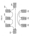
- FIG. 53 shows a system comprising four communication nodes 5201 to 5204.
- Communication modules 5012 loaded with optical transceivers and shared memories, are installed in the communication nodes 5201 to 5204, and the flow of frames F1 to F4 loaded with the respective data of the communication nodes 5201 to 5204, forms a logical ring topology.
- each communication node configures a leading part of the optical data signal with an unmodulated signal, modulates the unmodulated part of the optical data signal input to each communication node, and transmits the modulated optical data signal as the optical control signal for link query.
- multiple communication nodes can be connected at low cost and with high reliability, and sharing of the memories of the respective communication nodes becomes possible.
- an optical communication system comprising: multiple communication nodes each having a pair of a signal output port and a signal input port; and multiple path establishment circuits each having multiple optical input ports and multiple optical output ports which are set so that an optical signal input from an optical input port is output to a predetermined optical output port corresponding to the wavelength of the input optical signal, wherein the signal output port and the signal input port of the pair of each communication node are connected to an optical input port and an optical output port of one of the multiple path establishment circuits, an optical input port of one path establishment circuit is connected to an optical output port of another path establishment circuit, and an optical output port of the one path establishment circuit is connected to an optical input port of the other path establishment circuit.
- an optical communication system in an optical communication system according to a twentieth aspect of the present invention, in an optical communication system according to any of the tenth through nineteenth aspects, further comprising a management node which monitors and controls the condition of the respective communication nodes, wherein the respective communication nodes and the management node communicate using an optical signal, of which the wavelength is different from the wavelength of an optical data signal loaded with information of communication nodes.
- An optical communication system is an optical communication system for communicating between multiple communication nodes each having a pair of a signal output port and a signal input port, comprising: a path establishment circuit having multiple optical input ports and multiple optical output ports which is previously set so that an optical signal input from an optical input port is output to a predetermined optical output port depending on the wavelength of the input optical signal; a database prestored with output wavelengths used in the case in which a signal is routed from a predetermined optical input port to the predetermined optical output port in the path establishment circuit; and a controlling device which receives control information including a connection request from a communication node, refers to the database and reads out an output wavelength which should be set by the communication node, and transmits control information for instructing the output wavelength to the communication node which transmitted the connection request, wherein the signal output port and the signal input port of the pair of each multiple communication node are connected to an optical input port and an optical output port of the path establishment circuit, and an optical input port of one path establishment circuit
- a communication node means a device which receives an input optical signal, effects communication processing and then outputs an optical signal with a predetermined wavelength.
- Logical ring topology means a configuration where the logical connection forms a ring shape.
- Arrayed-waveguide grating means a passive functional device where an optical waveguide is formed on a substrate made of silica, silicon or the like. By means of an arrayed-waveguide grating, a path establishment modifying function, a wavelength selecting function and the like can be realized.
- a wavelength-tunable optical light source means an optical light source which can control and modify the wavelength of the output optical signal.
- N being the number of input ports and output ports of an N x N arrayed waveguide grating optical multiplexer/demultiplexer (hereunder, N x N-AWG) which functions as a wavelength path establishment circuit, and as n, being the number of communication nodes.
- N x N-AWG N arrayed waveguide grating optical multiplexer/demultiplexer
- n being the number of communication nodes.
- the invention is not limited to this and it may be such that N is any integer of 2 or more and that n is any integer of 2 or more and less than or equal to N.
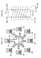
- FIG. 3A and FIG. 3B show a second embodiment of an optical communication system of the present invention.
- FIG. 3A shows a case with one route (same as the case of the first embodiment) and
- FIG. 3B shows a case with three routes.
- FIG. 9 shows another example of a configuration related to transfer of optical control signals in the respective communication nodes, together with an N x N-AWG.
- the example is shown for the case where a part of the optical data signal is split and transmitted as the optical control signal.
- the other configuration is the same as for the case of FIG. 8.
- FIG. 10 shows yet another example of a configuration related to transfer of optical control signals in the respective communication nodes, together with an N x N-AWG.
- FIG. 10 shown an example, as with the example in FIG. 9, of the case where a part of the optical data signal is simply split and returned to the input port.
- an optical data signal of a shared memory frame 901 of the communication node (#1) 201 is sent to the communication node (#2) 202, an unmodulated part at the head is split by the optical splitter 1802 of the communication node (#2) 202, modulated by the optical modulator 1102 and returned as a reverse optical data signal 2201 for link query, and sent to the communication node (#1) 201, and received by the reverse optical data signal receiver 2101.
- the communication node (#1) 201 similarly to the examples in FIG. 9 and FIG.
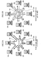
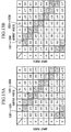
- FIG. 13A and FIG. 13B show an example of setting of wavelengths of optical data signals and optical control signals of the communication nodes in the case where a fault occurs.
- FIG. 13A shows a case where the used wavelength does not have cyclic characteristics
- FIG. 13B shows a case where the used wavelength has cyclic characteristics.
- reference symbols 1501 to 1508 are skip wavelengths for at the time of a fault. However, these wavelengths ( ⁇ 3, ⁇ 5, ⁇ 7, ⁇ 9, ⁇ 11, ⁇ 13, ⁇ 7, and ⁇ 9 in the case of FIG. 13A, and ⁇ 3, ⁇ 5, ⁇ 7, ⁇ 1, ⁇ 3, ⁇ 5, ⁇ 7, and ⁇ 1 in the case of FIG.
- the number of path establishment circuits for connection is four.
- the number of path establishment circuits for connection is not limited to the number described in the embodiment, and has no upper limit.
- An optical signal from the output circuit 3302 of the communication node 3202 is input to the input circuit 3411 of the communication node 3211 and received, and after communication processing by the communication node 3211, the optical signal is output from the output circuit 3311.
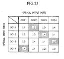
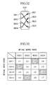
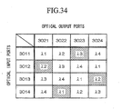
- an optical signal of ⁇ 3 wavelength is input from the optical input port 3011, it is output to the optical output port 3023. If an optical signal of ⁇ 2 wavelength is input from the optical input port 3013, it is output to the optical output port 3024. If an optical signal of ⁇ 4 wavelength is input from the optical input port 3014, it is output to the optical output port 3021.
- the wavelength of a communication node connected to the path establishment circuit 3101 in FIG. 26 is arranged such as in FIG. 27 or FIG. 28, it becomes possible in the path establishment circuit 3101 to establish the paths shown by the arrowheads in FIG. 26. In this manner, if the wavelength of the optical signal input to the optical input port of the path establishment circuit is modified, optional path establishment becomes feasible in the path establishment circuit.
- connection of the communication nodes circulates sequentially from the communication node 3201, the communication node 3211, the communication node 3204, the communication node 3205, the communication node 3212, the communication node 3203, to communication node 3201, so that the connection of these communication nodes forms a logical ring topology.
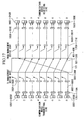
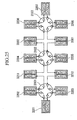
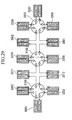
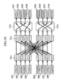
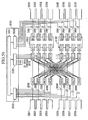
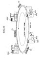
- FIG. 30 describes an optical communication system for accommodating eight communication nodes.
- reference symbols 3101 to 3103 denote path establishment circuits
- reference symbols 3201 to 3208 denote communication nodes
- reference symbols 3301 to 3308 denote respectively output circuits of the communication nodes 3201 to 3208
- reference symbols 3401 to 3408 denote respectively input circuits of the communication nodes 3201 to 3208
- reference symbols 3601 to 3608 denote optical switches
- reference symbols 3701 to 3708 denote optical multiplexers.
- FIG. 30 four communication nodes, four optical switches, four optical multiplexers, and one path establishment circuit constitute one unit, and an optical communication system comprises two units.
- the thin lines denote directions in which connections are possible by the optical switches
- the thick lines denote directions in which connections are actually made.
- An optical signal from the output circuit 3307 of the communication node 3207 is input via the optical switch 3607, the optical multiplexer 3707 and the path establishment circuit 3102 to the input circuit 3405 of the communication node 3205 and received, and after communication processing by the communication node 3205, the optical signal is output from the output circuit 3305.
- An optical signal from the output circuit 3305 of the communication node 3205 is input via the optical switch 3605, the optical multiplexer 3704 and the path establishment circuit 3101 to the input circuit 3402 of the communication node 3202 and received, and after communication processing by the communication node 3202, the optical signal is output from the output circuit 3302.
- An optical signal from the output circuit 3302 of the communication node 3202 is input via the optical switch 3602, the optical multiplexer 3708 and the path establishment circuit 3102 to the input circuit 3406 of the communication node 3206 and received, and after communication processing by the communication node 3206, the optical signal is output from the output circuit 3306.
- the optical input port and optical output port pairs of the path establishment circuit were described as four pairs, however the optical input port and optical output port pairs of the path establishment circuit are not limited to four pairs and may be multiple pairs.
- the path establishment circuits have the same number of optical input ports and optical output port pairs, however the respective path establishment circuits may have different numbers of optical input port and optical output port pairs.
- the above embodiment is configured by two units of path establishment circuits, however the number of units is not limited.
- the present embodiment is such that in the above-described embodiments, the communication node 3204 is replaced by the repeater 3501 and the communication node 3205 is replaced by the repeater 3502. Even if they are replaced in this manner, the connection of the communication nodes circulates sequentially from the communication node 3201, the communication node 3203, the repeater 3501, the communication node 3207, the repeater 3502, the communication node 3202, the communication node 3206, the communication node 3208, to the communication node 3201, so that the connection of these communication nodes forms a logical ring topology.
- the connection of FIG. 36 becomes equivalent to a connection skipping the communication nodes 3204 and 3205 in FIG. 31.
- an optical communication system for modifying the connections of the communication nodes, by modifying the wavelength of the optical signals from the output circuit of the communication node, and the direction of the optical switch.
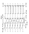
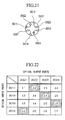
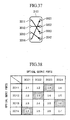
- FIG. 37 shows a configuration of a path establishment circuit.
- reference symbol 3101 denotes the path establishment circuit
- reference symbols 3011, 3012, 3013 and 3014 denote optical input ports
- reference symbols 3021, 3022, 3023 and 3024 denote optical output ports.
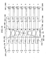
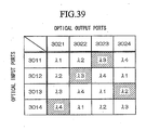
- FIG. 38 and FIG. 39 show wavelength-routing characteristics which determine from which optical output port an optical signal input from an optical input port is to be output corresponding to the wavelength thereof.
- FIG. 38 shows a case without cyclic-wavelength characteristics
- FIG. 39 shows a case with cyclic-wavelength characteristics.
- Such characteristic can be realized by configuring with an arrayed waveguide grating.
- the number of wavelengths used in the respective communication nodes may be only a few.
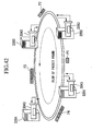
- FIG. 42 shows a basic configuration of an information sharing system comprising four communication nodes 3201 to 3204. Shared memory boards 3043 loaded with optical transceivers and memories are installed in the communication nodes 3201 to 3204.
- the flow of packet frames P1 to P4 loaded with information of the respective communication nodes 3201 to 3204 sent from the optical transceivers installed in the shared memory boards 3043 of the respective communication nodes for sharing information forms a logical ring topology.
- the packet frames P1 to P4 loaded with information of the respective communication nodes 3201 to 3204 circulate on a logical ring so that the respective communication nodes can share the information.
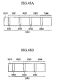
- FIG. 43A shows an example of the case where, the segment 3061 is information of the communication node 3201, the segment 3062 is information of the communication node 3202, the segment 3063 is information of the communication node 3203, and the segment 3064 is information of the communication node 3204.
- the frame configuration of the information sharing system and a method of loading information of the respective communication nodes onto the frames is not limited to those described above.
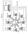
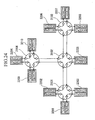
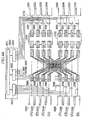
- FIG. 44 is a diagram showing a configuration of an information sharing system which uses the optical communication system of the present invention.
- only the signal lines which connect between the optical switch controlling section 3033 and the respective optical switches 3601 to 3608 are electric signal lines, and the other signal lines are signal lines configured by optical fibers.
- the input ports of the optical switch 360x (x is any integer from 1 to 8) are connected to the communication node 320x by optical fibers, and the output ports of the optical switches 3601 to 3608 are connected to the input ports of the corresponding 5 x 1 optical multiplexers 3701 to 3708 and the input ports of all of the optical multiplexers 3701 to 3708 connected to the other path establishment circuit.
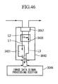
- the optical transceiver 3047 based on control information transmitted to the optical control/data signal transmitting/receiving board 3044 of the communication node via the optical control signal transmitting section 3034 of the network management node 3030 serving as an optical control/data signal related to a wavelength of the wavelength-tunable optical light source, sets the wavelength of the wavelength-tunable optical light source via the wavelength-tunable optical light source controlling section 3042 of the communication node, and outputs a packet frame as an optical packet frame signal of the desired wavelength ⁇ d in the 1.55 ⁇ m band.
- an optical packet frame signal transmitted from the wavelength-tunable optical light source built-in optical transceiver 3047 installed in the shared memory board 3043, and an optical control signal output from the optical transceiver 3052 loaded in the optical control/data signal transmitting/receiving board 3044, are multiplexed by the optical multiplexer 3053, and transmitted via an optical fiber to the optical demultiplexer 3090 shown in FIG. 44.
- an optical packet frame signal and an optical control signal, transmitted via the optical demultiplexer 3091 shown in FIG. 44 to a communication node by an optical fiber, are demultiplexed by the optical demultiplexer 3054.
- the shared memory board 3043 On the logical ring topology, when a packet frame (optical signal) from one of the adjacent communication nodes is input via an optical fiber to the optical receiving section of the optical transceiver 3047, the packet frame of the optical signal is converted into an electric signal.
- the frame transfer processing circuit 3432 splits the photo-electrically converted packet frame into two directions of a first direction L1 and a second direction L2. Regarding the packet frame split into the first direction L1, information of each of the communication nodes written in the packet frame is identified by the frame transfer processing circuit 3432, and information of the other communication nodes are respectively stored in the predetermined address space of the shared memory 3431 for respective communication nodes.
- the communication nodes transmit the information of the respective communication nodes stored in the shared memory 3431 to the image data signal processing section 3048 as required.
- the network management section 3031 is mainly configured by; a processor section 3035, a control signal input/output interface 3036, and a storage medium 3037.
- the storage medium 3037 there is registered as a basic database: a table of wavelength-routing characteristics of the path establishment circuit 3101 and the path establishment circuit 3102; information of the communication nodes connected to the input port side of the optical switches 3601 to 3608, and information of the input ports of the path establishment circuits connected via the optical multiplexers to the output port side of the optical switches 3601 to 3609.
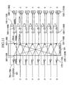
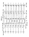
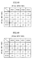
- FIG. 48 shows a table of wavelength-routing characteristics showing the relationship between the wavelengths of the path establishment circuit 3101 and the input/output ports.
- FIG. 49 shows a table of wavelength-routing characteristics showing the relationship between the wavelengths of the path establishment circuit 3102 and the input/output ports.
- An optical packet frame signal output from communication node 3205 passes through the optical switch 3605, the optical multiplexer 3704, the input port 3014 of the path establishment circuit 3101, the output port 3021 of the path establishment circuit and the optical multiplexer 3091, and is received by the optical transceiver 3047 of the shared memory board 3043 of the communication node 3201.
- the wavelength of the optical packet frame signal output from the communication node 3205 is set to ⁇ 4 based on the wavelength characteristics (FIG. 48) of the path establishment circuit 3101.
- an optical packet frame signal output from the communication node 3202 passes through the optical switch 3602, the optical multiplexer 3706, the input port 3016 of the path establishment circuit 3102, the output port 3028 of the path establishment circuit and the optical multiplexer 3091, and is received by the optical transceiver 3047 of the shared memory board 3043 of the communication node 3208.
- the wavelength of the optical packet frame signal output from the communication node 3201 is set to ⁇ 1 based on the wavelength-routing characteristics (FIG. 49) of the path establishment circuit 3102.
- connection of the communication nodes circulates sequentially from the communication node 3202 ⁇ the communication node 3206 ⁇ the communication node 3208, so that the connection of these communication nodes forms a logical ring topology.
- Mach-Zehnder type optical switches made of Silica-glass optical waveguides or the like are applicable, however, they are not limited to this as long as they are optical devices having a function for outputting an input optical signal to any one direction of eight directions.
- the optical communication system accommodating eight communication nodes shown in FIG. 44, a description is given of an embodiment related to fault avoidance in the case where a fault occurs.
- the configuration of the respective communication nodes is the same as in FIG. 45.
- the relationship between the wavelengths of the path establishment circuit 3101 and the path establishment circuit 3102 and the optical input/output ports is as shown in FIG. 48 and FIG. 49 respectively.
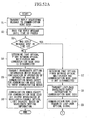
- the network management node 3030 in order to query the condition (presence of a disconnection) of an optical fiber 3123 for connecting the communication node 3203 and the optical multiplexer 3091, sends a reply requesting message from the optical control signal transmitting section 3034 to the communication node 3203 (step S1 of the flowchart in FIG. 52A).
- the network management node 3030 based on the relationship between the respective input/output ports and the wavelengths of the path establishment circuit 3101 and the path establishment circuit 3102 (FIG. 48 and FIG. 49); transmits wavelength setting information for setting the output wavelength of the wavelength-tunable optical light source of the optical transceiver 3047 of the communication node 3201 to ⁇ 4 and for optical outputting, from the optical control signal transmitting section 3034 to the communication node 3201; transmits wavelength setting information for setting the output wavelength of the wavelength-tunable optical light source of the optical transceiver 3047 of the communication node 3204 to ⁇ 3 and for optical outputting, from the optical control signal transmitting section 3034 to the communication node 3204; transmits wavelength setting information for setting the output wavelength of the wavelength-tunable optical light source of the optical transceiver 3047 of the communication node 3207 to ⁇ 3 and for optical outputting, from the optical control signal transmitting section 3034 to the communication node 3207; and transmits wavelength setting information for setting the output wavelength of
- the network management node 3030 transmits from the optical control signal transmitting section 3034 to the communication node 3203, instruction information for setting the output wavelength of its own wavelength-tunable optical light source to a wavelength for returning to its own communication node 3203, that is to ⁇ 1 (based on FIG. 48) and for optical outputting (hereunder, called "loop-back wavelength outputting instruction”) (step S8 in FIG. 52A).
- an optical packet frame for transmitting the information of the respective communication nodes sequentially circulates on a logical ring topology of the communication node 3201 ⁇ the communication node 3204 ⁇ the communication node 3207 ⁇ the communication node 3205 ⁇ the communication node 3201, so that it is possible to continue the operation of information sharing.
Landscapes
- Engineering & Computer Science (AREA)
- Computer Networks & Wireless Communication (AREA)
- Signal Processing (AREA)
- Optical Communication System (AREA)
Applications Claiming Priority (4)
| Application Number | Priority Date | Filing Date | Title |
|---|---|---|---|
| JP2002338242 | 2002-11-21 | ||
| JP2002338242 | 2002-11-21 | ||
| JP2003326317 | 2003-09-18 | ||
| JP2003326317 | 2003-09-18 |
Publications (3)
| Publication Number | Publication Date |
|---|---|
| EP1422967A2 true EP1422967A2 (de) | 2004-05-26 |
| EP1422967A3 EP1422967A3 (de) | 2006-07-26 |
| EP1422967B1 EP1422967B1 (de) | 2012-10-31 |
Family
ID=32232728
Family Applications (2)
| Application Number | Title | Priority Date | Filing Date |
|---|---|---|---|
| EP03104283A Withdrawn EP1422854A2 (de) | 2002-11-21 | 2003-11-19 | Optisches Übertragungssystem |
| EP03292883A Expired - Lifetime EP1422967B1 (de) | 2002-11-21 | 2003-11-20 | Optisches Vermittlungssystem |
Family Applications Before (1)
| Application Number | Title | Priority Date | Filing Date |
|---|---|---|---|
| EP03104283A Withdrawn EP1422854A2 (de) | 2002-11-21 | 2003-11-19 | Optisches Übertragungssystem |
Country Status (2)
| Country | Link |
|---|---|
| EP (2) | EP1422854A2 (de) |
| CN (1) | CN1503501A (de) |
Family Cites Families (2)
| Publication number | Priority date | Publication date | Assignee | Title |
|---|---|---|---|---|
| US6643463B1 (en) * | 1998-10-26 | 2003-11-04 | Nippon Telegraph And Telephone Corporation | Optical wavelength division multiplexing transmission network system using transmitting/receiving apparatuses having 2-input and 2-output optical path switching elements |
| JP3292843B2 (ja) * | 1998-10-26 | 2002-06-17 | 日本電信電話株式会社 | 光波長分割多重伝送ネットワーク装置 |
-
2003
- 2003-11-19 EP EP03104283A patent/EP1422854A2/de not_active Withdrawn
- 2003-11-19 CN CNA2003101163277A patent/CN1503501A/zh active Pending
- 2003-11-20 EP EP03292883A patent/EP1422967B1/de not_active Expired - Lifetime
Non-Patent Citations (1)
| Title |
|---|
| None |
Also Published As
| Publication number | Publication date |
|---|---|
| CN1503501A (zh) | 2004-06-09 |
| EP1422967B1 (de) | 2012-10-31 |
| EP1422967A3 (de) | 2006-07-26 |
| EP1422854A2 (de) | 2004-05-26 |
Similar Documents
| Publication | Publication Date | Title |
|---|---|---|
| US7072580B2 (en) | Autoprotected optical communication ring network | |
| EP0593039B1 (de) | Optischer Konzentrator und optisches Übertragungsnetz mit einem derartigen Konzentrator | |
| JP5545212B2 (ja) | 波長パス通信ノード装置、波長パス通信制御方法、プログラム、および記録媒体 | |
| US8280244B2 (en) | Optical ring network system | |
| JP3092521B2 (ja) | 通信ネットワークノード装置、光通信ネットワークノード装置、信号監視方式、及び、通信ネットワーク | |
| US7522837B2 (en) | Optical communication system | |
| JP2003298540A (ja) | データ伝送システム、光ネットワーク監視制御信号の伝送方法及びノード | |
| EP1056235A2 (de) | Optisches Ringsystem | |
| US6377725B1 (en) | Optical wavelength division multiplexed interconnect system providing autonomous information selection and prioritization | |
| US7054555B2 (en) | Communication network, wavelength division multiplex transmission equipment, optical switch equipment, and optical attribute/state administering method for them | |
| US20020105693A1 (en) | Optical transmission unit and system | |
| WO2011018926A1 (ja) | ネットワーク管理装置および波長パス設定方法 | |
| CN1666564B (zh) | 用于wdm网络的路径保护方法和相应的节点 | |
| US7805072B2 (en) | Wavelength division multiplex optical ring network for transmitting protected signals by local state switching following local interruption detection | |
| JP4598934B2 (ja) | 光伝送装置および光伝送システム | |
| EP1422967B1 (de) | Optisches Vermittlungssystem | |
| JP2002141867A (ja) | 波長多重光信号送信装置、波長多重光信号受信装置および光波長多重通信システム | |
| JP4488813B2 (ja) | 直接的に接続された光学素子を管理するための方法及びシステム | |
| JP3971331B2 (ja) | 光波長分割多重伝送ネットワーク装置、波長ルータおよび送受信装置 | |
| JP3730202B2 (ja) | 光ネットワークシステム | |
| JP3683791B2 (ja) | 光ネットワークシステム | |
| JP2005117603A (ja) | 光通信方式 | |
| JP2004254339A (ja) | 通信ネットワーク及び通信ネットワーク・ノード装置 | |
| JPH11112422A (ja) | 波長多重網切替え装置及び波長多重リング光ネットワーク・システム | |
| JP3363603B2 (ja) | 格子型ネットワークシステム及びノード間接続装置 |
Legal Events
| Date | Code | Title | Description |
|---|---|---|---|
| PUAI | Public reference made under article 153(3) epc to a published international application that has entered the european phase |
Free format text: ORIGINAL CODE: 0009012 |
|
| 17P | Request for examination filed |
Effective date: 20031126 |
|
| AK | Designated contracting states |
Kind code of ref document: A2 Designated state(s): AT BE BG CH CY CZ DE DK EE ES FI FR GB GR HU IE IT LI LU MC NL PT RO SE SI SK TR |
|
| AX | Request for extension of the european patent |
Extension state: AL LT LV MK |
|
| PUAL | Search report despatched |
Free format text: ORIGINAL CODE: 0009013 |
|
| AK | Designated contracting states |
Kind code of ref document: A3 Designated state(s): AT BE BG CH CY CZ DE DK EE ES FI FR GB GR HU IE IT LI LU MC NL PT RO SE SI SK TR |
|
| AX | Request for extension of the european patent |
Extension state: AL LT LV MK |
|
| AKX | Designation fees paid |
Designated state(s): DE FR GB |
|
| 17Q | First examination report despatched |
Effective date: 20110131 |
|
| GRAC | Information related to communication of intention to grant a patent modified |
Free format text: ORIGINAL CODE: EPIDOSCIGR1 |
|
| GRAP | Despatch of communication of intention to grant a patent |
Free format text: ORIGINAL CODE: EPIDOSNIGR1 |
|
| GRAC | Information related to communication of intention to grant a patent modified |
Free format text: ORIGINAL CODE: EPIDOSCIGR1 |
|
| RIN1 | Information on inventor provided before grant (corrected) |
Inventor name: NOGUCHI, KAZUTO Inventor name: TANOBE, HIROMASA Inventor name: MATSUOKA, MORITO Inventor name: SAKAMOTO, TAKASHI Inventor name: OKADA, AKIRA Inventor name: MORIWAKI, OSAMU |
|
| GRAS | Grant fee paid |
Free format text: ORIGINAL CODE: EPIDOSNIGR3 |
|
| GRAA | (expected) grant |
Free format text: ORIGINAL CODE: 0009210 |
|
| AK | Designated contracting states |
Kind code of ref document: B1 Designated state(s): DE FR GB |
|
| REG | Reference to a national code |
Ref country code: GB Ref legal event code: FG4D |
|
| RIN1 | Information on inventor provided before grant (corrected) |
Inventor name: MORIWAKI, OSAMU Inventor name: TANOBE, HIROMASA Inventor name: NOGUCHI, KAZUTO Inventor name: MATSUOKA, MORITO Inventor name: SAKAMOTO, TAKASHI Inventor name: OKADA, AKIRA |
|
| REG | Reference to a national code |
Ref country code: DE Ref legal event code: R096 Ref document number: 60342474 Country of ref document: DE Effective date: 20121227 |
|
| PLBE | No opposition filed within time limit |
Free format text: ORIGINAL CODE: 0009261 |
|
| STAA | Information on the status of an ep patent application or granted ep patent |
Free format text: STATUS: NO OPPOSITION FILED WITHIN TIME LIMIT |
|
| 26N | No opposition filed |
Effective date: 20130801 |
|
| REG | Reference to a national code |
Ref country code: DE Ref legal event code: R097 Ref document number: 60342474 Country of ref document: DE Effective date: 20130801 |
|
| PGFP | Annual fee paid to national office [announced via postgrant information from national office to epo] |
Ref country code: FR Payment date: 20141110 Year of fee payment: 12 Ref country code: DE Payment date: 20141111 Year of fee payment: 12 Ref country code: GB Payment date: 20141119 Year of fee payment: 12 |
|
| REG | Reference to a national code |
Ref country code: DE Ref legal event code: R119 Ref document number: 60342474 Country of ref document: DE |
|
| GBPC | Gb: european patent ceased through non-payment of renewal fee |
Effective date: 20151120 |
|
| REG | Reference to a national code |
Ref country code: FR Ref legal event code: ST Effective date: 20160729 |
|
| PG25 | Lapsed in a contracting state [announced via postgrant information from national office to epo] |
Ref country code: GB Free format text: LAPSE BECAUSE OF NON-PAYMENT OF DUE FEES Effective date: 20151120 Ref country code: DE Free format text: LAPSE BECAUSE OF NON-PAYMENT OF DUE FEES Effective date: 20160601 |
|
| PG25 | Lapsed in a contracting state [announced via postgrant information from national office to epo] |
Ref country code: FR Free format text: LAPSE BECAUSE OF NON-PAYMENT OF DUE FEES Effective date: 20151130 |