EP1420457B1 - Manufacturing method of an insulated gate power semiconductor device with Schottky diode - Google Patents
Manufacturing method of an insulated gate power semiconductor device with Schottky diode Download PDFInfo
- Publication number
- EP1420457B1 EP1420457B1 EP02425695A EP02425695A EP1420457B1 EP 1420457 B1 EP1420457 B1 EP 1420457B1 EP 02425695 A EP02425695 A EP 02425695A EP 02425695 A EP02425695 A EP 02425695A EP 1420457 B1 EP1420457 B1 EP 1420457B1
- Authority
- EP
- European Patent Office
- Prior art keywords
- layer
- dopant
- implanted
- drain
- body region
- Prior art date
- Legal status (The legal status is an assumption and is not a legal conclusion. Google has not performed a legal analysis and makes no representation as to the accuracy of the status listed.)
- Expired - Lifetime
Links
- 239000004065 semiconductor Substances 0.000 title claims description 24
- 238000004519 manufacturing process Methods 0.000 title claims description 14
- 239000002019 doping agent Substances 0.000 claims description 45
- 238000000034 method Methods 0.000 claims description 41
- 229910021420 polycrystalline silicon Inorganic materials 0.000 claims description 38
- 210000004027 cell Anatomy 0.000 claims description 37
- 229920005591 polysilicon Polymers 0.000 claims description 35
- 239000000758 substrate Substances 0.000 claims description 33
- 230000008569 process Effects 0.000 claims description 29
- 239000007943 implant Substances 0.000 claims description 26
- 210000000746 body region Anatomy 0.000 claims description 25
- 238000005468 ion implantation Methods 0.000 claims description 24
- 229920002120 photoresistant polymer Polymers 0.000 claims description 23
- 238000005530 etching Methods 0.000 claims description 21
- 238000002513 implantation Methods 0.000 claims description 19
- 238000000151 deposition Methods 0.000 claims description 18
- 230000008021 deposition Effects 0.000 claims description 8
- 239000003989 dielectric material Substances 0.000 claims description 7
- 230000004888 barrier function Effects 0.000 claims description 6
- 125000006850 spacer group Chemical group 0.000 claims description 6
- 230000015572 biosynthetic process Effects 0.000 claims description 5
- 229910052751 metal Inorganic materials 0.000 claims description 5
- 239000002184 metal Substances 0.000 claims description 5
- 230000000873 masking effect Effects 0.000 claims description 4
- 230000003213 activating effect Effects 0.000 claims 4
- 238000010438 heat treatment Methods 0.000 claims 4
- 238000009792 diffusion process Methods 0.000 description 14
- XUIMIQQOPSSXEZ-UHFFFAOYSA-N Silicon Chemical compound [Si] XUIMIQQOPSSXEZ-UHFFFAOYSA-N 0.000 description 13
- 229910052710 silicon Inorganic materials 0.000 description 13
- 239000010703 silicon Substances 0.000 description 13
- ZOXJGFHDIHLPTG-UHFFFAOYSA-N Boron Chemical compound [B] ZOXJGFHDIHLPTG-UHFFFAOYSA-N 0.000 description 9
- 229910052796 boron Inorganic materials 0.000 description 9
- 229910052738 indium Inorganic materials 0.000 description 9
- APFVFJFRJDLVQX-UHFFFAOYSA-N indium atom Chemical compound [In] APFVFJFRJDLVQX-UHFFFAOYSA-N 0.000 description 9
- 239000000463 material Substances 0.000 description 9
- 238000000206 photolithography Methods 0.000 description 9
- 108091006146 Channels Proteins 0.000 description 8
- 230000001413 cellular effect Effects 0.000 description 7
- 230000004913 activation Effects 0.000 description 6
- 230000008901 benefit Effects 0.000 description 6
- 239000013078 crystal Substances 0.000 description 6
- 239000011810 insulating material Substances 0.000 description 6
- 229910052785 arsenic Inorganic materials 0.000 description 4
- RQNWIZPPADIBDY-UHFFFAOYSA-N arsenic atom Chemical compound [As] RQNWIZPPADIBDY-UHFFFAOYSA-N 0.000 description 4
- 150000002500 ions Chemical class 0.000 description 4
- 230000010287 polarization Effects 0.000 description 4
- 230000009467 reduction Effects 0.000 description 4
- 208000032365 Electromagnetic interference Diseases 0.000 description 3
- RTAQQCXQSZGOHL-UHFFFAOYSA-N Titanium Chemical compound [Ti] RTAQQCXQSZGOHL-UHFFFAOYSA-N 0.000 description 3
- 238000013459 approach Methods 0.000 description 3
- 238000010884 ion-beam technique Methods 0.000 description 3
- 230000000670 limiting effect Effects 0.000 description 3
- 238000012856 packing Methods 0.000 description 3
- 238000011084 recovery Methods 0.000 description 3
- 239000010936 titanium Substances 0.000 description 3
- 229910052719 titanium Inorganic materials 0.000 description 3
- BPQQTUXANYXVAA-UHFFFAOYSA-N Orthosilicate Chemical compound [O-][Si]([O-])([O-])[O-] BPQQTUXANYXVAA-UHFFFAOYSA-N 0.000 description 2
- 239000000969 carrier Substances 0.000 description 2
- 210000003850 cellular structure Anatomy 0.000 description 2
- 230000005684 electric field Effects 0.000 description 2
- 238000005516 engineering process Methods 0.000 description 2
- 238000007667 floating Methods 0.000 description 2
- 230000003071 parasitic effect Effects 0.000 description 2
- 230000002829 reductive effect Effects 0.000 description 2
- 230000002441 reversible effect Effects 0.000 description 2
- 108010075750 P-Type Calcium Channels Proteins 0.000 description 1
- 230000002411 adverse Effects 0.000 description 1
- 230000015556 catabolic process Effects 0.000 description 1
- 239000002131 composite material Substances 0.000 description 1
- 230000009977 dual effect Effects 0.000 description 1
- 230000000694 effects Effects 0.000 description 1
- 229910052737 gold Inorganic materials 0.000 description 1
- 230000001678 irradiating effect Effects 0.000 description 1
- 230000004807 localization Effects 0.000 description 1
- 238000001465 metallisation Methods 0.000 description 1
- 229910052697 platinum Inorganic materials 0.000 description 1
- 238000000926 separation method Methods 0.000 description 1
- 229910021332 silicide Inorganic materials 0.000 description 1
- FVBUAEGBCNSCDD-UHFFFAOYSA-N silicide(4-) Chemical compound [Si-4] FVBUAEGBCNSCDD-UHFFFAOYSA-N 0.000 description 1
- 230000001360 synchronised effect Effects 0.000 description 1
- 238000009827 uniform distribution Methods 0.000 description 1
Images


Classifications
-
- H—ELECTRICITY
- H01—ELECTRIC ELEMENTS
- H01L—SEMICONDUCTOR DEVICES NOT COVERED BY CLASS H10
- H01L29/00—Semiconductor devices adapted for rectifying, amplifying, oscillating or switching, or capacitors or resistors with at least one potential-jump barrier or surface barrier, e.g. PN junction depletion layer or carrier concentration layer; Details of semiconductor bodies or of electrodes thereof ; Multistep manufacturing processes therefor
- H01L29/66—Types of semiconductor device ; Multistep manufacturing processes therefor
- H01L29/66007—Multistep manufacturing processes
- H01L29/66075—Multistep manufacturing processes of devices having semiconductor bodies comprising group 14 or group 13/15 materials
- H01L29/66227—Multistep manufacturing processes of devices having semiconductor bodies comprising group 14 or group 13/15 materials the devices being controllable only by the electric current supplied or the electric potential applied, to an electrode which does not carry the current to be rectified, amplified or switched, e.g. three-terminal devices
- H01L29/66409—Unipolar field-effect transistors
- H01L29/66477—Unipolar field-effect transistors with an insulated gate, i.e. MISFET
- H01L29/66674—DMOS transistors, i.e. MISFETs with a channel accommodating body or base region adjoining a drain drift region
- H01L29/66712—Vertical DMOS transistors, i.e. VDMOS transistors
- H01L29/66719—With a step of forming an insulating sidewall spacer
-
- H—ELECTRICITY
- H01—ELECTRIC ELEMENTS
- H01L—SEMICONDUCTOR DEVICES NOT COVERED BY CLASS H10
- H01L21/00—Processes or apparatus adapted for the manufacture or treatment of semiconductor or solid state devices or of parts thereof
- H01L21/02—Manufacture or treatment of semiconductor devices or of parts thereof
- H01L21/04—Manufacture or treatment of semiconductor devices or of parts thereof the devices having at least one potential-jump barrier or surface barrier, e.g. PN junction, depletion layer or carrier concentration layer
- H01L21/18—Manufacture or treatment of semiconductor devices or of parts thereof the devices having at least one potential-jump barrier or surface barrier, e.g. PN junction, depletion layer or carrier concentration layer the devices having semiconductor bodies comprising elements of Group IV of the Periodic System or AIIIBV compounds with or without impurities, e.g. doping materials
- H01L21/26—Bombardment with radiation
- H01L21/263—Bombardment with radiation with high-energy radiation
- H01L21/265—Bombardment with radiation with high-energy radiation producing ion implantation
- H01L21/26586—Bombardment with radiation with high-energy radiation producing ion implantation characterised by the angle between the ion beam and the crystal planes or the main crystal surface
-
- H—ELECTRICITY
- H01—ELECTRIC ELEMENTS
- H01L—SEMICONDUCTOR DEVICES NOT COVERED BY CLASS H10
- H01L29/00—Semiconductor devices adapted for rectifying, amplifying, oscillating or switching, or capacitors or resistors with at least one potential-jump barrier or surface barrier, e.g. PN junction depletion layer or carrier concentration layer; Details of semiconductor bodies or of electrodes thereof ; Multistep manufacturing processes therefor
- H01L29/66—Types of semiconductor device ; Multistep manufacturing processes therefor
- H01L29/66007—Multistep manufacturing processes
- H01L29/66075—Multistep manufacturing processes of devices having semiconductor bodies comprising group 14 or group 13/15 materials
- H01L29/66227—Multistep manufacturing processes of devices having semiconductor bodies comprising group 14 or group 13/15 materials the devices being controllable only by the electric current supplied or the electric potential applied, to an electrode which does not carry the current to be rectified, amplified or switched, e.g. three-terminal devices
- H01L29/66409—Unipolar field-effect transistors
- H01L29/66477—Unipolar field-effect transistors with an insulated gate, i.e. MISFET
- H01L29/66674—DMOS transistors, i.e. MISFETs with a channel accommodating body or base region adjoining a drain drift region
- H01L29/66712—Vertical DMOS transistors, i.e. VDMOS transistors
-
- H—ELECTRICITY
- H01—ELECTRIC ELEMENTS
- H01L—SEMICONDUCTOR DEVICES NOT COVERED BY CLASS H10
- H01L29/00—Semiconductor devices adapted for rectifying, amplifying, oscillating or switching, or capacitors or resistors with at least one potential-jump barrier or surface barrier, e.g. PN junction depletion layer or carrier concentration layer; Details of semiconductor bodies or of electrodes thereof ; Multistep manufacturing processes therefor
- H01L29/66—Types of semiconductor device ; Multistep manufacturing processes therefor
- H01L29/68—Types of semiconductor device ; Multistep manufacturing processes therefor controllable by only the electric current supplied, or only the electric potential applied, to an electrode which does not carry the current to be rectified, amplified or switched
- H01L29/76—Unipolar devices, e.g. field effect transistors
- H01L29/772—Field effect transistors
- H01L29/78—Field effect transistors with field effect produced by an insulated gate
- H01L29/7801—DMOS transistors, i.e. MISFETs with a channel accommodating body or base region adjoining a drain drift region
- H01L29/7802—Vertical DMOS transistors, i.e. VDMOS transistors
- H01L29/7803—Vertical DMOS transistors, i.e. VDMOS transistors structurally associated with at least one other device
- H01L29/7806—Vertical DMOS transistors, i.e. VDMOS transistors structurally associated with at least one other device the other device being a Schottky barrier diode
-
- H—ELECTRICITY
- H01—ELECTRIC ELEMENTS
- H01L—SEMICONDUCTOR DEVICES NOT COVERED BY CLASS H10
- H01L29/00—Semiconductor devices adapted for rectifying, amplifying, oscillating or switching, or capacitors or resistors with at least one potential-jump barrier or surface barrier, e.g. PN junction depletion layer or carrier concentration layer; Details of semiconductor bodies or of electrodes thereof ; Multistep manufacturing processes therefor
- H01L29/66—Types of semiconductor device ; Multistep manufacturing processes therefor
- H01L29/68—Types of semiconductor device ; Multistep manufacturing processes therefor controllable by only the electric current supplied, or only the electric potential applied, to an electrode which does not carry the current to be rectified, amplified or switched
- H01L29/76—Unipolar devices, e.g. field effect transistors
- H01L29/772—Field effect transistors
- H01L29/78—Field effect transistors with field effect produced by an insulated gate
- H01L29/7839—Field effect transistors with field effect produced by an insulated gate with Schottky drain or source contact
-
- H—ELECTRICITY
- H01—ELECTRIC ELEMENTS
- H01L—SEMICONDUCTOR DEVICES NOT COVERED BY CLASS H10
- H01L29/00—Semiconductor devices adapted for rectifying, amplifying, oscillating or switching, or capacitors or resistors with at least one potential-jump barrier or surface barrier, e.g. PN junction depletion layer or carrier concentration layer; Details of semiconductor bodies or of electrodes thereof ; Multistep manufacturing processes therefor
- H01L29/66—Types of semiconductor device ; Multistep manufacturing processes therefor
- H01L29/86—Types of semiconductor device ; Multistep manufacturing processes therefor controllable only by variation of the electric current supplied, or only the electric potential applied, to one or more of the electrodes carrying the current to be rectified, amplified, oscillated or switched
- H01L29/861—Diodes
- H01L29/872—Schottky diodes
-
- H—ELECTRICITY
- H01—ELECTRIC ELEMENTS
- H01L—SEMICONDUCTOR DEVICES NOT COVERED BY CLASS H10
- H01L29/00—Semiconductor devices adapted for rectifying, amplifying, oscillating or switching, or capacitors or resistors with at least one potential-jump barrier or surface barrier, e.g. PN junction depletion layer or carrier concentration layer; Details of semiconductor bodies or of electrodes thereof ; Multistep manufacturing processes therefor
- H01L29/02—Semiconductor bodies ; Multistep manufacturing processes therefor
- H01L29/06—Semiconductor bodies ; Multistep manufacturing processes therefor characterised by their shape; characterised by the shapes, relative sizes, or dispositions of the semiconductor regions ; characterised by the concentration or distribution of impurities within semiconductor regions
- H01L29/08—Semiconductor bodies ; Multistep manufacturing processes therefor characterised by their shape; characterised by the shapes, relative sizes, or dispositions of the semiconductor regions ; characterised by the concentration or distribution of impurities within semiconductor regions with semiconductor regions connected to an electrode carrying current to be rectified, amplified or switched and such electrode being part of a semiconductor device which comprises three or more electrodes
- H01L29/0843—Source or drain regions of field-effect devices
- H01L29/0847—Source or drain regions of field-effect devices of field-effect transistors with insulated gate
- H01L29/0852—Source or drain regions of field-effect devices of field-effect transistors with insulated gate of DMOS transistors
- H01L29/0873—Drain regions
- H01L29/0878—Impurity concentration or distribution
-
- H—ELECTRICITY
- H01—ELECTRIC ELEMENTS
- H01L—SEMICONDUCTOR DEVICES NOT COVERED BY CLASS H10
- H01L29/00—Semiconductor devices adapted for rectifying, amplifying, oscillating or switching, or capacitors or resistors with at least one potential-jump barrier or surface barrier, e.g. PN junction depletion layer or carrier concentration layer; Details of semiconductor bodies or of electrodes thereof ; Multistep manufacturing processes therefor
- H01L29/02—Semiconductor bodies ; Multistep manufacturing processes therefor
- H01L29/06—Semiconductor bodies ; Multistep manufacturing processes therefor characterised by their shape; characterised by the shapes, relative sizes, or dispositions of the semiconductor regions ; characterised by the concentration or distribution of impurities within semiconductor regions
- H01L29/10—Semiconductor bodies ; Multistep manufacturing processes therefor characterised by their shape; characterised by the shapes, relative sizes, or dispositions of the semiconductor regions ; characterised by the concentration or distribution of impurities within semiconductor regions with semiconductor regions connected to an electrode not carrying current to be rectified, amplified or switched and such electrode being part of a semiconductor device which comprises three or more electrodes
- H01L29/1095—Body region, i.e. base region, of DMOS transistors or IGBTs
-
- H—ELECTRICITY
- H01—ELECTRIC ELEMENTS
- H01L—SEMICONDUCTOR DEVICES NOT COVERED BY CLASS H10
- H01L29/00—Semiconductor devices adapted for rectifying, amplifying, oscillating or switching, or capacitors or resistors with at least one potential-jump barrier or surface barrier, e.g. PN junction depletion layer or carrier concentration layer; Details of semiconductor bodies or of electrodes thereof ; Multistep manufacturing processes therefor
- H01L29/40—Electrodes ; Multistep manufacturing processes therefor
- H01L29/41—Electrodes ; Multistep manufacturing processes therefor characterised by their shape, relative sizes or dispositions
- H01L29/417—Electrodes ; Multistep manufacturing processes therefor characterised by their shape, relative sizes or dispositions carrying the current to be rectified, amplified or switched
- H01L29/41725—Source or drain electrodes for field effect devices
- H01L29/41766—Source or drain electrodes for field effect devices with at least part of the source or drain electrode having contact below the semiconductor surface, e.g. the source or drain electrode formed at least partially in a groove or with inclusions of conductor inside the semiconductor
-
- H—ELECTRICITY
- H01—ELECTRIC ELEMENTS
- H01L—SEMICONDUCTOR DEVICES NOT COVERED BY CLASS H10
- H01L29/00—Semiconductor devices adapted for rectifying, amplifying, oscillating or switching, or capacitors or resistors with at least one potential-jump barrier or surface barrier, e.g. PN junction depletion layer or carrier concentration layer; Details of semiconductor bodies or of electrodes thereof ; Multistep manufacturing processes therefor
- H01L29/66—Types of semiconductor device ; Multistep manufacturing processes therefor
- H01L29/66007—Multistep manufacturing processes
- H01L29/66075—Multistep manufacturing processes of devices having semiconductor bodies comprising group 14 or group 13/15 materials
- H01L29/66227—Multistep manufacturing processes of devices having semiconductor bodies comprising group 14 or group 13/15 materials the devices being controllable only by the electric current supplied or the electric potential applied, to an electrode which does not carry the current to be rectified, amplified or switched, e.g. three-terminal devices
- H01L29/66409—Unipolar field-effect transistors
- H01L29/66477—Unipolar field-effect transistors with an insulated gate, i.e. MISFET
- H01L29/66674—DMOS transistors, i.e. MISFETs with a channel accommodating body or base region adjoining a drain drift region
- H01L29/66712—Vertical DMOS transistors, i.e. VDMOS transistors
- H01L29/66727—Vertical DMOS transistors, i.e. VDMOS transistors with a step of recessing the source electrode
Definitions
- the invention relates to insulated gate planar integrated power devices and in particular to devices to which is associated a power diode integrated on the same chip.
- the intrinsic bipolar diode (body-drain junction) is switched, but such an intrinsic diode is inefficient because:
- a known approach is that of using a Schottky diode of the same voltage and of appropriate area, in parallel to the internal PN junction diode of the integrated structure of the insulated gate device (for example a power MOS transistor or briefly PMOS).
- the Schottky diode Because of the absence of minority carriers, the Schottky diode is characterized by a fast recovery and, because of the different barrier heights, it has lower conduction voltages. In fact, for voltages lower than 0.9V the Schottky diode conducts a larger current than a PN junction diode; for higher voltages, the characteristics become similar and the PN diode finally conducts a larger current, because of the a modulation of its conductivity.
- Figure 1 illustrates the advantage of a combined diode MPS (Merged PN Schottky) in respect to a normal junction diode.
- a more efficient solution depicted in Figure 4 , consists in "distributing" the Schottky diode uniformly over the whole active area of the PMOS by integrating it in the elementary cells of the MOS. It has been demonstrated that by using a uniform distribution of Schottky diodes, it is possible to improve the dynamic performances ( trr and softness) while using a reduced total area dedicated to the diode.
- Schottky diode is realized in the elementary cell of the MOSFET by a dedicated step of photolithography for realizing a Schottky diode through a certain aperture produced through a first deposited polysilicon layer, that is in the area destined to the realization of the integrated structure of an elementary cell of the insulated gate power device and on which the relative source contact will be established.
- Schottky diodes are realized by contacting with a metal layer the monocrystalline semiconductor substrate, the doping level of which determines the voltage class.
- the technique of forming, around the Schottky contact region in the semiconductor, a more or less dense array of juxtaposed diffuse regions (tubs) of opposite type of conductivity to that of the substrate (Lateral Merged PiN Schottky).
- the distance of separation among adjacent tubs is chosen so that under conditions of inverse polarization, the electric field is partially shielded by the depleted zones that form around the tubs.
- the US patent No. 4,823,172 discloses a vertical MOSFET including a N epitaxial layer grown on a P+ or N+ substrate, a P type channel region and a N+ source region, having a Schottky diode formed between the N epitaxial layer and a metal source electrode extending through the source region and the channel region and reaching the epitaxial layer under the source and channel regions for preventing latch-up of a parasitic thyristor.
- a further and more general objective is that of limiting the number of photolithographic steps in the sequence of process steps of an insulated gate integrated power device with co-integrated Schottky diode in parallel thereto.
- the photolithographic step for defining the Schottky contact area inside the aperture of a discrete or of an elementary cell of an integrated structure of the insulated gate power device is eliminated by carrying out:
- the invention provides a method for integrating a Schottky contact inside the apertures of the elementary cells that constitute the integrated structure of the insulated gate power device in a totally self-alignment manner without requiring a dedicated masking step.
- the process of this invention differs from the known processes for the realization of a structure of an insulated gate device with Schottky diode integrated in the elementary cells that compose the device, because of the way in which the elementary cell structure is realized such to include a Schottky contact between the source metal layer and a region of semiconductor crystal of substrate electrically coinciding with the drain of the integrated power device.
- process steps that characterize the invention may be introduced in any process flow for the fabrication of an integrated floating gate power device, such as a power MOS or briefly PMOS. For this reason, specific dimensional details of structural features and relative doses and implantation energies of the dopants are not indicated, given that these may vary from a process to another depending on fabrication technology, particular needs and/or preferences of the manufacturer.
- an implantation (which hereinafter will be referred to as of "drain engineering" or D.E.) is included in the process sequence for increasing the resistivity of the semiconductor of substrate (drain) of the device under the Schottky contact region.
- the semiconductor substrate of drain may be in practice an epitomical layer grown on a semiconductor crystal that may have electrical characteristics different from those of the epitaxial layer grown thereon.
- An implanted buried region of "drain engineering" will be electrically tied to the body or, where they exists, to the deep body diffusions, such to effectively shield the Schottky contact also in a vertical direction, with the result of decisively reducing the leakage current.
- the realized integrated structure may be defined as "Lateral & Vertical Merged PiN Schottky (LVMPS)".
- the invention has been illustrated for the case of fabrication of a N channel PMOS, the invention can be practiced also for fabricating a P channel PMOS, by inverting the types of dopants.
- stripe layout is not mandatory, other cellular layouts may be used, eventually performing several pairs of body implantations each with appropriate tilts and twist angles in order to realize the body diffusions in each channel zone while defining a Shottky contact window there between.
- a self-aligned Schottky contact in a "window" defined by the use of angled implantations in the middle of the cell area may be extended even to a structure with traditional contacts (that is defined and opened by photolithography).
- the etching of silicon for forming the microtrench will not be self-aligned to the window opened by photolithography through the polysilicon, but self-aligned to the contact openings.
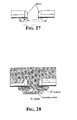
- the graph of Figure 30 shows the leakage current and the direct voltage drop obtained on test structures for different doses of drain engineering dopant. Near the dose of 2* 10 12 ions/cm 2 there is enough room for reducing the leakage by an order of magnitude without burdening excessively the direct voltage drop. By doubling the dose, the drain engineering diffusion creates a junction that shields the Schottky contact but reduces the direct characteristic to become practically similar to that of a PN junction diode.
Description
- The invention relates to insulated gate planar integrated power devices and in particular to devices to which is associated a power diode integrated on the same chip.
- Insulated gate devices, such as MOSFETs in particular, are used in many applications as synchronous rectifiers. In this case, the insulated gate device operates as a diode: it is turned on when the equivalent diode must be in conduction and is turned off when the diode must stop conducting.
- This happens for example in output bridge stages in DC-DC converter applications.
- In these applications, the intrinsic bipolar diode (body-drain junction) is switched, but such an intrinsic diode is inefficient because:
- it switches slowly;
- it has a high conduction voltage;
- it may generate EMI in the board
- In order to reduce the switching time or more precisely the reverse recovery time of the diode (trr), techniques for controlling the life time of minority carriers are generally used. The introduction in the semiconductor substrate of the device of Au, Pt, or other elements by ion implantation, or irradiation with electrons, produces a marked decrease of the life time (from tens of microseconds to tens of nanoseconds) with consequent reduction of the trr of the intrinsic or internal diode. In any case, the reduction of the trr is accompanied by an increase of the conduction voltage (Vf) and of the output resistance (Ron) of the insulated gate device that limits the usefulness of such techniques.
- Moreover, these techniques amplify or do not reduce the problems due to a too fast recovery of the diode and thus to the emissions of electromagnetic interferences (EMI) on the board. In order to improve softness, more complex alternative techniques are needed.
- A known approach is that of using a Schottky diode of the same voltage and of appropriate area, in parallel to the internal PN junction diode of the integrated structure of the insulated gate device (for example a power MOS transistor or briefly PMOS).
- Because of the absence of minority carriers, the Schottky diode is characterized by a fast recovery and, because of the different barrier heights, it has lower conduction voltages. In fact, for voltages lower than 0.9V the Schottky diode conducts a larger current than a PN junction diode; for higher voltages, the characteristics become similar and the PN diode finally conducts a larger current, because of the a modulation of its conductivity.
- Therefore, the parallel of a junction diode and a Schottky diode produces an equivalent device with the following characteristics:
- reduced Vf at relatively low current levels (<0.8V);
- less stored charge and thus reduction of the switching time.
-
Figure 1 illustrates the advantage of a combined diode MPS (Merged PN Schottky) in respect to a normal junction diode. - The experimental trade-off curve between Vf and the inverse current peak during the switching of a MPS diode upon varying the area of the Schottky diode and when the control of the life time in a PN diode has been obtained by irradiating the junction will high energy electrons (3MeV) at doses comprised between 0 and 32 MRad.
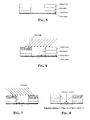
- Nowadays, various Schottky diode configurations, in parallel with the intrinsic diode of the PMOS structure are implemented in planar devices to be used in the low voltage range (320 - 150 V): that is from the simplest architecture that uses a single package but separate devices (discrete solution) depicted in
Figure 2 , to more complex architectures that integrate the Schottky diode in the PMOS structure itself. - Among known "integrated" solutions, there is the one shown in
Figure 3 , according to which a separated area (on the same chip) is dedicated for the Schottky diode. However, this solution has limitations and drawbacks, as will be explained later. - A more efficient solution, depicted in
Figure 4 , consists in "distributing" the Schottky diode uniformly over the whole active area of the PMOS by integrating it in the elementary cells of the MOS. It has been demonstrated that by using a uniform distribution of Schottky diodes, it is possible to improve the dynamic performances (trr and softness) while using a reduced total area dedicated to the diode. - A solution of this kind, for low voltages devices, is disclosed in the
US Patent No. 5,886,383 . - According to the technique described in the patent, Schottky diode is realized in the elementary cell of the MOSFET by a dedicated step of photolithography for realizing a Schottky diode through a certain aperture produced through a first deposited polysilicon layer, that is in the area destined to the realization of the integrated structure of an elementary cell of the insulated gate power device and on which the relative source contact will be established.
- Commonly, Schottky diodes are realized by contacting with a metal layer the monocrystalline semiconductor substrate, the doping level of which determines the voltage class. In order to improve electric characteristics (leakage and breakdown voltage) when not conducting, it is well known the technique of forming, around the Schottky contact region in the semiconductor, a more or less dense array of juxtaposed diffuse regions (tubs) of opposite type of conductivity to that of the substrate (Lateral Merged PiN Schottky). The distance of separation among adjacent tubs is chosen so that under conditions of inverse polarization, the electric field is partially shielded by the depleted zones that form around the tubs.
- Summarizing, in order to co-integrate Schottky diodes within the cellular structure of a power MOS there are two different approaches:
- 1) Schottky diode formed in dedicated areas inside the power MOS. In this case, areas more or less distributed are defined within the active area of the MOS structure, on which a Schottky contact is realized through the process steps that are done for realizing the integrated MOS structure. As explained before, in order to limit leakage current, the Schottky diode contact is surrounded by diffusions of opposite type of conductivity to that of the semiconductor crystal for shielding the electric field that is created under inverse polarization. The shielding diffusions may be realized by the same body implant of the MOS or by a dedicated implant step.
- 2) Schottky diode integrated in the single elementary cells that constitute the power MOS. Even if more efficient, this approach is little used because it imposes layout restraints severely limiting the possibility of increasing the packing density. The known techniques, such as the technique described in the above mentioned
US Patent No. 5,886,383 , require the realization of an island (51 ofFigure 6 ) of oxide or photoresist within an aperture produced through the polysilicon layer (poly). This limits the possibility of reducing the width of the aperture and represents an obstacle to increase the packing density of the elementary cells of the integrated structure of the power device. The shielding diffusions of the Schottky diode must necessarily be realized with the same implant step of the body of the MOS. - The
US patent No. 4,823,172 discloses a vertical MOSFET including a N epitaxial layer grown on a P+ or N+ substrate, a P type channel region and a N+ source region, having a Schottky diode formed between the N epitaxial layer and a metal source electrode extending through the source region and the channel region and reaching the epitaxial layer under the source and channel regions for preventing latch-up of a parasitic thyristor. - There exists the need of integrating a Schottky diode in an elementary cell of an integrated structure of an insulated gate power device without limiting the possibility of reducing the dimensions (scaling down) of the elementary cell apart from the resolution of the photo-exposition equipment and the precision of localization of the dopants implanted in the semiconductor substrate crystal of the available fabrication technology.
- A further and more general objective is that of limiting the number of photolithographic steps in the sequence of process steps of an insulated gate integrated power device with co-integrated Schottky diode in parallel thereto.
- The above mentioned objectives and other important advantages are obtained with the fabrication process of the present invention.
- According to the present disclosure, the photolithographic step for defining the Schottky contact area inside the aperture of a discrete or of an elementary cell of an integrated structure of the insulated gate power device, is eliminated by carrying out:
- 1) an ion implantation of dopants for realizing a diffused body region with appropriate tilt and twist angles through the cell aperture formed in the layer of polysilicon deposited beforehand;
- 2) an ion implantation of dopants for realizing a source diffusion on the whole area of the aperture through the polysilicon;
- 3) formation of a spacer along the lateral walls of the cell aperture through the polysilicon to define the anisotropic etching area of the semiconductor crystal.
- In practice, the invention provides a method for integrating a Schottky contact inside the apertures of the elementary cells that constitute the integrated structure of the insulated gate power device in a totally self-alignment manner without requiring a dedicated masking step. This overcomes the above indicated limits to the possibility of increasing the packing density of the cellular structure of the integrated power device, while permitting improved performances of the co-integrated Schottky diode under inverse polarization of the device and producing other advantages that will be mentioned in the ensuing description.
- The invention and the various embodiments thereof are more precisely defined in the annexed claims.
- The different aspects and advantages of this invention will appear even more evident through the following description of several alternative embodiments and referring to the attached drawings wherein:
-
Figure 1 shows the experimental trade-off curve between the voltage Vf and the inverse current peak of a switching MPS diode, with an irradiated PN junction diode in function of the area reserved to the Schottky diode; -
Figure 2 depicts a solution with discrete elements combined in a single package; -
Figure 3 depicts a monolithic solution with distinct areas for the PMOS and the Schottky diode; -
Figure 4 depicts an integrated solution of a Schottky diode in each elementary cell of the PMOS, according to the prior art; - Figures from 5 to 14 illustrate the relevant steps of a process of fabrication of an insulated gate power device according to a first embodiment of this invention; and characteristics of the structure that is realized;
- Figures from 15 to 21 illustrate the relevant steps of a process of fabrication according to a second embodiment of this invention; and characteristics of the structure that is realized;
-
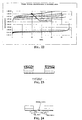
Figure 22 shows leakage characteristics under inverse polarization in function of the area of the Schottky contact; - Figures from 23 to 29 illustrate the relevant steps of a process of fabrication according to a third embodiment of this invention; and characteristics of the structure that is realized;
-
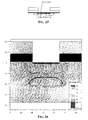
Figure 30 shows the inverse leakage and the direct voltage drop performances in function of the characteristics of a shielding buried region of the Schottky contact. - Making reference to the Figures, the integrated structure and the way in which it may be realized according to preferred embodiments of this invention will be described herein below.
- Basically, the process of this invention differs from the known processes for the realization of a structure of an insulated gate device with Schottky diode integrated in the elementary cells that compose the device, because of the way in which the elementary cell structure is realized such to include a Schottky contact between the source metal layer and a region of semiconductor crystal of substrate electrically coinciding with the drain of the integrated power device.
- The process steps that characterize the invention may be introduced in any process flow for the fabrication of an integrated floating gate power device, such as a power MOS or briefly PMOS. For this reason, specific dimensional details of structural features and relative doses and implantation energies of the dopants are not indicated, given that these may vary from a process to another depending on fabrication technology, particular needs and/or preferences of the manufacturer.
- Moreover, only for illustrating purposes, the realization of a N-channel PMOS is shown, though it is intended that the disclosed structure may also be that of a P-channel floating gate device, by simply inverting, in a dual mode, the type of conductivity of the semiconductor crystal substrate and of the dopants used for realizing the various diffused regions.
-
- 1. realization of the drain semiconductor substrate and of the edge structure of the integrated insulated gate power device according to any known process;
- 2. realization of the insulated gate according to any known process (growth or deposition of a dielectric gate oxide film and deposition thereon of a conducting layer of polycrystalline silicon (polysilicon));
- 3. covering of the conducting gate electrode layer of polysilicon with an insulating layer of a dielectric material (for example a layer of 0.5 µm of LTO);
- 4. covering with photosensitive material of appropriate thickness (for example a layer of 1.5 µm of a photoresist);
- 5. definition of the gate electrode of polysilicon by photolithography of the layer photoresist followed by selective anisotropic etching first of the insulating layer and then of the polysilicon (on grounds of expediency a stripe cellular layout may be preferable (that is each cell is defined in the form of a short segment of a definition line, but of course the process may be practiced with any other type of cellular layout);
- 6. ion implantation (first body implant) with appropriate tilt and twist angles of a P type dopant (for example boron or indium with 30° tilt and 90° twist). The tilt angle must be chosen such to create a not implanted shade zone by the windows opened by the anisotropic (vertical) etching in the stack composed of the polysilicon layer and the insulating layer. The tilt angle to be used will depend from the total height of the etched edge of the hard mask formed by the polysilicon the insulating layer and eventually also of the residual thickness of the photo resist mask, and from the width of the stripes or definition lines. The twist angle must be such to make the impinging ion beam orthogonal to the long side of the stripe segments. The implant dose and energy will be chosen such to obtain the desired concentration and channel length;
- 7. ion implantation (second body implantation) of the same P type dopant but with tilt and twist angles opposite to the ones of the preceding implantation step (for example boron or indium with -30° tilt and 90° twist or 30° tilt and -90° twist);
- 8. removing of the mask of photoresist;
- 9. activation of the body dopants (for example, 30 seconds in oven at 1100°C);
- 10. ion implantation (source implant) of a N type dopant (for example 1015 ions/cm2 of arsenic with an implant energy of about 80 keV);
- 11. activation of the source dopant (for example, 30 seconds in oven at 1100°C);
- 12. covering with one or more layers of a dielectric insulating material deposited in a sufficient conformal mode on the cell area definition steps;
- 13. anisotropic (vertical) etching of the layer of insulating material deposited for forming a spacer over the definition edges of the cell area stripes;
- 14. anisotropic (vertical) etching of the silicon for a depth deeper than the depth of the doped source region but shallower than the depth of the doped body regions. The so realized microtrench exposes within the area of each cell of the integrated structure of the PMOS, silicon surfaces of the doped source regions, the doped body regions and at the bottom of the trench also the surface of the silicon of substrate between the body diffusions, that coincides electrically with the drain of the PMOS;
- 15. opening by means of a dedicated photolithography of the gate contacts;
- 16. metallization of the front side of the wafer with a material capable of establishing a good electrical contact with said exposed surfaces of the body and source diffusions and a good barrier height of the Schottky contact that is established at the bottom of the trench with the silicon of substrate, that is with the drain of the integrated structure of the insulated gate power device (suitable materials may be for example titanium or a silicide thereof);
- 17. finishing of the front side and of the rear side according to the common fabrication process.
- Even if it is possible to realize the body regions with only two tilted implantations, it may happen that the charge under the source be insufficient in certain particular applications to prevent the turning on of the parasitic transistor that is created by the source/body/drain junctions.
- In order to increase robustness, it is advisable for certain applications to perform a second pair of tilted implantations for enriching the body zones under the source, in practice realizing a second or deep body diffused region.
-
- 1. realization of the drain semiconductor substrate and of the edge structure of the integrated insulated gate power device according to any known process;
- 2. realization of the insulated gate according to any known process (growth or deposition of a dielectric gate oxide film and deposition thereon of a conducting layer of polycrystalline silicon (polysilicon));
- 3. covering of the conducting gate electrode layer of polysilicon with an insulating layer of a dielectric material (for example a layer of 0.5 µm of LTO);
- 4. covering with photosensitive material of appropriate thickness (for example a layer of 1.5 µm of a photo resist);
- 5. definition of the gate electrode of polysilicon by photolithography of the layer photo resist followed by selective anisotropic etching first of the insulating layer and then of the polysilicon (on grounds of expediency a stripe cellular layout may be preferable (that is each cell is defined in the form of a short segment of a definition line, but of course the process may be practiced with any other type of cellular layout);
- 6. ion implantation (first deep body implantation) with appropriate tilt and twist angles of a P type dopant (for example boron or indium with 20° tilt and 90° twist). The tilt angle must be chosen such to create a not implanted shade zone in the windows opened by the anisotropic (vertical) etching through the stack composed of the polysilicon layer and the insulating layer. The tilt angle to be used will depend from the total height of the etched edge of the mask formed by the polysilicon layer, the insulating layer and the residual thickness of the photo resist mask, and from the width of the stripes or definition lines. The twist angle must be such that the ionic stream be orthogonal to the long side of the stripes. The dose and the implant energy must be chosen such to obtain the desired concentration;
- 7. ion implantation (second deep body implant) of the same P type dopant but with tilt and twist angles opposite to those of the preceding implantation step (for example boron or indium with -20° tilt and 90° twist or 20° tilt and -90° twist);
- 8. removing of the mask of photo resist;
- 9. ion implantation (first body implant) with appropriate tilt and twist angles of a P type dopant (for example boron or indium with 40° tilt and 90° twist). The tilt angle must be chosen such to create a not implanted shade zone by the windows opened by the anisotropic (vertical) etching in the stack composed of the polysilicon layer and the insulating layer. The tilt angle to be used will depend from the total height of the etched edge of the hard mask formed by the polysilicon the insulating layer and from the width of the stripes or definition lines. The twist angle must be such to make the impinging ion beam orthogonal to the long side of the stripe segments. The implant dose and energy will be chosen such to obtain the desired concentration and channel length;
- 10. ion implantation (second body implantation) of the same P type dopant but with tilt and twist angles opposite to those of the preceding implantation step (for example boron or indium with -40° tilt and 90° twist or 40° tilt and -90° twist);
- 11. activation of the dopants (for example, 30 seconds in an oven at 1100°C);
- 12. ion implantation (source implant) of a N type dopant (for example 1015 ions/cm2 of arsenic with an implant energy of 80 keV);
- 13. activation of the source dopant (for example, 30 seconds in oven at 1100°C);
- 14. covering with one or more layers of a dielectric insulating material deposited in a sufficient conformal mode on the cell area definition steps;
- 15. anisotropic (vertical) etching of the layer of insulating material deposited for forming a spacer over the definition edges of the cell area stripes;
- 16. anisotropic (vertical) etching of the silicon for a depth deeper than the depth of the doped source region but shallower than the depth of the doped body regions. The so realized micro trench exposes within the area of each cell of the integrated structure of the PMOS, silicon surfaces of the doped source regions, the doped body regions and at the bottom of the trench also the surface of the silicon of substrate between the body diffusions, that coincides electrically with the drain of the PMOS;
- 17. opening by means of a dedicated photolithography of the gate contacts;
- 18. moralization of the front side of the wafer with a material capable of establishing a good electrical contact with said exposed surfaces of the body and source diffusions and a good barrier height of the Schottky contact that is established at the bottom of the trench with the silicon of substrate, that is with the drain of the integrated structure of the insulated gate power device (suitable materials may be for example titanium or a silicate thereof);
- 19. finishing of the front side and of the rear side according to the common fabrication process.
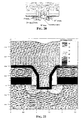
- It has been noticed that the presence of a Schottky contact sensibly worsen the reverse bias electrical characteristics of the integrated device. As may be observed from the characteristics of
Figure 22 , the leakage current varies by orders of magnitude in function of the percentage of cell area that is dedicated to the Schottky contact. - In order to reduce the adverse effect on the leakage current of the presence of a co-integrated Schottky diode, according to an optional but highly preferred embodiment of this invention, an implantation (which hereinafter will be referred to as of "drain engineering" or D.E.) is included in the process sequence for increasing the resistivity of the semiconductor of substrate (drain) of the device under the Schottky contact region.
- Of course, the semiconductor substrate of drain may be in practice an epitomical layer grown on a semiconductor crystal that may have electrical characteristics different from those of the epitaxial layer grown thereon.
- An implanted buried region of "drain engineering" will be electrically tied to the body or, where they exists, to the deep body diffusions, such to effectively shield the Schottky contact also in a vertical direction, with the result of decisively reducing the leakage current.
- According to this optional but highly preferred embodiment, the realized integrated structure may be defined as "Lateral & Vertical Merged PiN Schottky (LVMPS)".
-
- 1. realization of the drain semiconductor substrate and of the edge structure of the integrated insulated gate power device according to any known process;
- 2. realization of the insulated gate according to any known process (growth or deposition of a dielectric gate oxide film and deposition thereon of a conducting layer of polycrystalline silicon (polysilicon));
- 3. covering of the conducting gate electrode layer of polysilicon with an insulating layer of a dielectric material (for example a layer of 0.5 µm of LTO);
- 4. covering with photosensitive material of appropriate thickness (for example a layer of 1.5 µm of a photo resist);
- 5. definition of the gate electrode of polysilicon by photolithography of the layer photo resist followed by selective anisotropic etching first of the insulating layer and then of the polysilicon (on grounds of expediency a stripe cellular layout may be preferable (that is each cell is defined in the form of a short segment of a definition line, but of course the process may be practiced with any other type of cellular layout);
- 6. ion implantation (Drain Engineering implant) at high energy of a P type dopant (for example boron at 200-400keV). The dose to be implanted must be such to compensate slightly the epitaxial layer and it is thus function of the voltage class of the power device being fabricated;
- 7. ion implantation (first body implant) with appropriate tilt and twist angles of a P type dopant (for example boron or indium with 30° tilt and 90° twist). The tilt angle must be chosen such to create a not implanted shade zone by the windows opened by the anisotropic (vertical) etching in the stack composed of the polysilicon layer and the insulating layer. The tilt angle to be used will depend from the total height of the etched edge of the hard mask formed by the polysilicon the insulating layer and eventually also of the residual thickness of the photo resist mask, and from the width of the stripes or definition lines. The twist angle must be such to make the impinging ion beam orthogonal to the long side of the stripe segments. The implant dose and energy will be chosen such to obtain the desired concentration and channel length;
- 8. ion implantation (second body implant) of the same P type dopant but with tilt and twist angles opposite to those of the preceding implantation (for example boron or indium with -30° tilt and 90° twist or 30° tilt and -90° twist);
- 9. removing of the mask of photo resist;
- 10. activation of the body dopants (for example, 30 seconds in oven at 1100°C);
- 11. ion implantation (source implant) of a N type dopant (for example 1015 ions/cm2 of arsenic with an implant energy of about 80 keV);
- 12. activation of the source dopant (for example, 30 seconds in oven at 1100°C);
- 13. covering with one or more layers of a dielectric insulating material deposited in a sufficient conformal mode on the cell area definition steps;
- 14. anisotropic (vertical) etching of the layer of insulating material deposited for forming a spacer over the definition edges of the cell area stripes;
- 15. anisotropic (vertical) etching of the silicon for a depth deeper than the depth of the doped source region but shallower than the depth of the doped body regions. The so realized micro trench exposes within the area of each cell of the integrated structure of the PMOS, silicon surfaces of the doped source regions, the doped body regions and at the bottom of the trench also the surface of the silicon of substrate between the body diffusions, that coincides electrically with the drain of the PMOS;
- 16. opening by means of a dedicated photolithography of the gate contacts;
- 17. moralization of the front side of the wafer with a material capable of establishing a good electrical contact with said exposed surfaces of the body and source diffusions and a good barrier height of the Schottky contact that is established at the bottom of the trench with the silicon of substrate, that is with the drain of the integrated structure of the insulated gate power device (suitable materials may be for example titanium or a silicate thereof);
- 18. finishing of the front side and of the rear side according to the common fabrication process.
- Advantages:
- a) the disclosed composite basic cell structure MOS+Schottky is realized without any additional dedicated masking step. The width of the stripes is thus limited only by the resolution of the photoexposition equipment and by the ability of precisely implant the dopants (to this end it is convenient to use dopants with low diffusivity such as indium and arsenic);
- b) by carrying out a process flow that contemplates the formation of an additional buried drain engineering region, a reduction of the leakage current of even an order of magnitude may be achieved while retaining all advantages under direct bias (
Figure 30 ). - Though the invention has been illustrated for the case of fabrication of a N channel PMOS, the invention can be practiced also for fabricating a P channel PMOS, by inverting the types of dopants.
- Of course, the use of a stripe layout is not mandatory, other cellular layouts may be used, eventually performing several pairs of body implantations each with appropriate tilts and twist angles in order to realize the body diffusions in each channel zone while defining a Shottky contact window there between.
- The formation of a self-aligned Schottky contact in a "window" defined by the use of angled implantations in the middle of the cell area, may be extended even to a structure with traditional contacts (that is defined and opened by photolithography). In this case the etching of silicon for forming the microtrench will not be self-aligned to the window opened by photolithography through the polysilicon, but self-aligned to the contact openings.
- Even the concept of "Lateral & Vertical Merged PiN Schottky (LVMPS)", that is the introduction of an implantation (buried region) under the lateral body diffusions and under the Schottky contact region, for modifying locally the doping profile of the drain, may be extended also to Schottky diodes that are not co-integrated in the elementary cells of the integrated power device, but realized in dedicated areas.
- The graph of
Figure 30 shows the leakage current and the direct voltage drop obtained on test structures for different doses of drain engineering dopant. Near the dose of 2* 1012 ions/cm2 there is enough room for reducing the leakage by an order of magnitude without burdening excessively the direct voltage drop. By doubling the dose, the drain engineering diffusion creates a junction that shields the Schottky contact but reduces the direct characteristic to become practically similar to that of a PN junction diode.
Claims (4)
- A process for fabricating an insulated gate integrated power device comprising the steps of:a) constituting a drain semiconductor substrate doped with a dopant of a first type of conductivity and forming an edge structure of the insulated gate integrated power device,b) forming an insulated gate electrode by growing or depositing a dielectric film of gate oxide on the surface of said drain semiconductor substrate and depositing thereon a conductive layer of polysilicon,c) covering said conductive polysilicon layer with an insulating layer or multilayer of dielectric material deposited thereon,d) depositing a layer of photo resist on said deposited insulating layer,e) defming said gate electrode by masking and anisotropic selective etching of said deposited insulating layer and of said polysilicon layer forming apertures through the area of which the integrated structure and the relative source contact of each elementary cell constituting said power device will be formed,
and characterized by the successive steps of:f) performing a first ion implantation of a dopant appropriate to constitute a body region of opposite type of conductivity of said drain semiconductor substrate with certain tilt and twist angles such to determine a not implanted shade zone inside said aperture in function of the total height of the definition edge of the stack composed of said polysilicon layer, said insulating layer and said layer of photo resist, and of the width of the aperture, with an implant dose and energy appropriate to obtain a certain concentration and channel length;g) performing at least a second ion implantation at the same conditions of said first implantation but with different tilt and twist angles to define a not implanted central window in the shade pattern on the implanted cell area;h) removing said layer of photo resist;i) activating the implanted dopants by heat treatment;j) performing a source ion implantation on the whole area of said aperture of a dopant of the same type of conductivity of the drain substrate and opposite to that of the dopant of said body implantations with dose and energy of implant appropriate to constitute a source region surrounded by said body region;k) activating of the implanted source dopant by heat treatment;l) depositing a sacrificial layer of a dielectric material under conditions of substantial uniformity of thickness of deposition over the steps of the definition borders of said apertures;m) anisotropic etching of the sacrificial layer for leaving a dielectric spacer on the definition edge surfaces of said apertures;n) anisotropic etching of the semiconductor for a depth deeper than the depth of said source region but shallower than the depth of said body region, exposing within the area of each cell surfaces of said source region, of said body region and, at the bottom of the trench, a zone of said drain substrate surrounded laterally by said body region;o) opening of contacts on said gate electrode through a dedicated photo resist mask;p) removing the photo resist mask and depositing one or more conductive metal layers for establishing inside said trench an electric contact with both the source region and the body region and determining a barrier height of the Schottky contact established with the drain substrate on at least a portion of the bottom surface of said trench. - A process for fabricating an insulated gate integrated power device comprising the steps of:a) constituting a drain semiconductor substrate doped with a dopant of a first type of conductivity and forming an edge structure of the insulated gate integrated power device,b) forming an insulated gate electrode by growing or depositing a dielectric film of gate oxide on the surface of said drain semiconductor substrate and depositing thereon a conductive layer of polysilicon,c) covering said conductive polysilicon layer with an insulating layer or multilayer of dielectric material deposited thereon,d) depositing a layer of photo resist on said deposited insulating layer,e) defining said gate electrode by masking and anisotropic selective etching of said deposited insulating layer and of said polysilicon layer forming apertures through the area of which the integrated structure and the relative source contact of each elementary cell constituting said power device will be formed, and characterized by the successive steps off) performing a first ion implantation of a dopant appropriate to constitute deep body region of opposite type of conductivity of said drain semiconductor substrate with certain tilt and twist angles such to determine a not implanted shade zone inside said aperture in function of the total height of the definition edge of the stack composed of said polysilicon layer, said insulating layer and said layer of photo resist, and of the width of the aperture, with an implant dose and energy appropriate to obtain a certain concentration and depth of implant;g) performing at least a second ion implantation at the same conditions of said first implantation but with different tilt and twist angles to define a central not implanted window in the shade pattern on the implanted cell area;h) removing said layer of photo resist;i) performing at least a third ion implantation of a dopant appropriate to constitute a body region of opposite type of conductivity of said drain semiconductor
substrate with certain tilt and twist angles such to determine a not implanted shade zone inside said aperture in function of the total height of the definition edge of the stack composed of said polysilicon layer and said insulating layer,
and of the width of the aperture, with an implant dose and energy appropriate to obtain a certain concentration and channel length;j) performing at least a fourth ion implantation at the same conditions of said third implantation but with different tilt and twist angles to define a central not implanted. window in the shade pattern on the implanted cell areak) activating the implanted body and deep body dopants by heat treatment;l) performing a source ion implantation on the whole area of said aperture of a dopant of the same type of conductivity of the drain substrate and opposite to that of the dopants of said body and deep body implantations, with dose and energy of implant appropriate to constitute a source region surrounded by said body region;m) activating the implanted source dopant by heat treatment;n) depositing a sacrificial layer of a dielectric material under conditions of substantial uniformity of thickness of deposition over the steps of the definition borders of said apertures;o) anisotropic etching of the sacrificial layer for leaving a dielectric spacer on the definition edge surfaces of said apertures;p) anisotropic etching of the semiconductor for a depth deeper than the depth of said source region but shallower than the depth of said body region, exposing within the area of each cell surfaces of said source region, of said body region, and, at the bottom of the trench, said deep body region and a zone of said drain substrate surrounded laterally by said deep body region;q) opening of contacts on said gate electrode through a dedicated photo resist mask;r) removing the photo resist mask and depositing one or more conductive metal layers for establishing inside said trench an electric contact with both the source region and the body region and determining a barrier height of the Schottky contact established with the drain substrate on at least a portion of the bottom surface of said trench. - A process of fabrication of a device according to claim 1 or 2, characterized in that it comprises the further step of carrying out, after having defined the gate electrode with the formation of said apertures, an ion implantation at sufficiently high energy for implanting a dopant of the same type of conductivity of the dopant used for realizing said body region in a buried region at a depth deeper than the bottom of said body regions, with a dose such to slightly overcompensate or undercompensate the dopant concentration of opposite type of conductivity of said drain substrate to create a shielding region under the Shottky contact.
- A process of fabrication of a device according to claim 3, characterized in that said dose of implanted dopant is insufficient to compensate completely the dopant concentration of opposite type of conductivity of said drain substrate.
Priority Applications (4)
| Application Number | Priority Date | Filing Date | Title |
|---|---|---|---|
| EP02425695A EP1420457B1 (en) | 2002-11-14 | 2002-11-14 | Manufacturing method of an insulated gate power semiconductor device with Schottky diode |
| EP10180038.1A EP2259327B1 (en) | 2002-11-14 | 2002-11-14 | Insulated gate power semiconductor device with Schottky diode and manufacturing method thereof |
| US10/713,778 US20040164304A1 (en) | 2002-11-14 | 2003-11-14 | Insulated gate planar integrated power device with co-integrated schottky diode and process |
| US11/520,210 US7560368B2 (en) | 2002-11-14 | 2006-09-12 | Insulated gate planar integrated power device with co-integrated Schottky diode and process |
Applications Claiming Priority (1)
| Application Number | Priority Date | Filing Date | Title |
|---|---|---|---|
| EP02425695A EP1420457B1 (en) | 2002-11-14 | 2002-11-14 | Manufacturing method of an insulated gate power semiconductor device with Schottky diode |
Related Child Applications (2)
| Application Number | Title | Priority Date | Filing Date |
|---|---|---|---|
| EP10180038.1A Division EP2259327B1 (en) | 2002-11-14 | 2002-11-14 | Insulated gate power semiconductor device with Schottky diode and manufacturing method thereof |
| EP10180038.1 Division-Into | 2010-09-27 |
Publications (2)
| Publication Number | Publication Date |
|---|---|
| EP1420457A1 EP1420457A1 (en) | 2004-05-19 |
| EP1420457B1 true EP1420457B1 (en) | 2012-01-11 |
Family
ID=32116366
Family Applications (2)
| Application Number | Title | Priority Date | Filing Date |
|---|---|---|---|
| EP10180038.1A Expired - Lifetime EP2259327B1 (en) | 2002-11-14 | 2002-11-14 | Insulated gate power semiconductor device with Schottky diode and manufacturing method thereof |
| EP02425695A Expired - Lifetime EP1420457B1 (en) | 2002-11-14 | 2002-11-14 | Manufacturing method of an insulated gate power semiconductor device with Schottky diode |
Family Applications Before (1)
| Application Number | Title | Priority Date | Filing Date |
|---|---|---|---|
| EP10180038.1A Expired - Lifetime EP2259327B1 (en) | 2002-11-14 | 2002-11-14 | Insulated gate power semiconductor device with Schottky diode and manufacturing method thereof |
Country Status (2)
| Country | Link |
|---|---|
| US (2) | US20040164304A1 (en) |
| EP (2) | EP2259327B1 (en) |
Families Citing this family (40)
| Publication number | Priority date | Publication date | Assignee | Title |
|---|---|---|---|---|
| US7294882B2 (en) * | 2004-09-28 | 2007-11-13 | Sandisk Corporation | Non-volatile memory with asymmetrical doping profile |
| DE102004057235B4 (en) * | 2004-11-26 | 2007-12-27 | Infineon Technologies Ag | Vertical trench transistor and method for its production |
| EP1742271A1 (en) * | 2005-07-08 | 2007-01-10 | STMicroelectronics S.r.l. | Power field effect transistor and manufacturing method thereof |
| US8080848B2 (en) * | 2006-05-11 | 2011-12-20 | Fairchild Semiconductor Corporation | High voltage semiconductor device with lateral series capacitive structure |
| US7618867B2 (en) | 2006-07-26 | 2009-11-17 | Infineon Technologies Ag | Method of forming a doped portion of a semiconductor and method of forming a transistor |
| US20080296636A1 (en) * | 2007-05-31 | 2008-12-04 | Darwish Mohamed N | Devices and integrated circuits including lateral floating capacitively coupled structures |
| US7807555B2 (en) * | 2007-07-31 | 2010-10-05 | Intersil Americas, Inc. | Method of forming the NDMOS device body with the reduced number of masks |
| JP2009218580A (en) * | 2008-03-06 | 2009-09-24 | Toshiba Corp | Bidirectional halo injection |
| US8193565B2 (en) | 2008-04-18 | 2012-06-05 | Fairchild Semiconductor Corporation | Multi-level lateral floating coupled capacitor transistor structures |
| WO2011033550A1 (en) * | 2009-09-15 | 2011-03-24 | 株式会社 東芝 | Semiconductor device |
| US8368140B2 (en) * | 2009-12-03 | 2013-02-05 | Diodes Incorporated | Trench MOS device with Schottky diode and method for manufacturing same |
| US8624302B2 (en) * | 2010-02-05 | 2014-01-07 | Fairchild Semiconductor Corporation | Structure and method for post oxidation silicon trench bottom shaping |
| TWI425575B (en) * | 2010-07-09 | 2014-02-01 | Tzu Hsiung Chen | Low gate charging rectifier having mos structure and p-n junction, and method of manufacturing the same |
| DE102010051874A1 (en) | 2010-11-22 | 2012-05-24 | Init Innovative Informatikanwendungen In Transport-, Verkehrs- Und Leitsystemen Gmbh | Circuit for protection against reverse polarity |
| EP2500848A1 (en) | 2011-03-15 | 2012-09-19 | Amadeus S.A.S. | Method and system for centralized reservation context management on multi-server reservation system |
| US8716825B2 (en) * | 2011-06-22 | 2014-05-06 | Macronix International Co., Ltd. | Semiconductor structure and manufacturing method for the same |
| CN102842596B (en) * | 2011-06-22 | 2015-05-20 | 旺宏电子股份有限公司 | Semiconductor structure and manufacturing method thereof |
| US8736013B2 (en) | 2012-04-19 | 2014-05-27 | Fairchild Semiconductor Corporation | Schottky diode with opposite-polarity schottky diode field guard ring |
| US20130313570A1 (en) * | 2012-05-24 | 2013-11-28 | Microsemi Corporation | Monolithically integrated sic mosfet and schottky barrier diode |
| US9018048B2 (en) | 2012-09-27 | 2015-04-28 | Stmicroelectronics S.R.L. | Process for manufactuirng super-barrier rectifiers |
| WO2014061724A1 (en) | 2012-10-19 | 2014-04-24 | 日産自動車株式会社 | Semiconductor device and method for manufacturing same |
| WO2014168430A1 (en) * | 2013-04-10 | 2014-10-16 | 주식회사 실리콘웍스 | Method for manufacturing rectifier circuit |
| CN104518006B (en) * | 2014-07-01 | 2017-03-15 | 重庆中科渝芯电子有限公司 | A kind of deplection type channel super barrier rectifier and its manufacture method |
| WO2016179025A1 (en) * | 2015-05-01 | 2016-11-10 | The Regents Of The University Of California | Enhanced patterning of integrated circuit layer by tilted ion implantation |
| CN106257626B (en) * | 2015-06-19 | 2019-05-14 | 北大方正集团有限公司 | Schottky device production method and schottky device |
| US10600871B2 (en) | 2016-05-23 | 2020-03-24 | General Electric Company | Electric field shielding in silicon carbide metal-oxide-semiconductor (MOS) device cells using body region extensions |
| DE102016111940B4 (en) * | 2016-06-29 | 2019-07-25 | Infineon Technologies Austria Ag | A method of manufacturing a superjunction semiconductor device and superjunction semiconductor device |
| CN106098752A (en) * | 2016-07-25 | 2016-11-09 | 吉林华微电子股份有限公司 | A kind of IGBT device and manufacture method thereof |
| US9941171B1 (en) * | 2016-11-18 | 2018-04-10 | Monolithic Power Systems, Inc. | Method for fabricating LDMOS with reduced source region |
| CN107154346B (en) * | 2017-05-19 | 2021-03-16 | 京东方科技集团股份有限公司 | Film doping method, thin film transistor and manufacturing method thereof |
| CN108899364B (en) * | 2018-07-02 | 2020-06-16 | 电子科技大学 | MOS (metal oxide semiconductor) grid-controlled thyristor integrated with Schottky diode and preparation method thereof |
| CN110212026B (en) * | 2019-05-06 | 2022-09-16 | 上海功成半导体科技有限公司 | Super junction MOS device structure and preparation method thereof |
| EP3742476A1 (en) * | 2019-05-20 | 2020-11-25 | Infineon Technologies AG | Method of implanting an implant species into a substrate at different depths |
| WO2020252306A1 (en) * | 2019-06-14 | 2020-12-17 | Silcotek Corp. | Nano-wire growth |
| CN112864222B (en) * | 2019-11-27 | 2022-04-12 | 苏州东微半导体股份有限公司 | Semiconductor power device |
| CN112864150B (en) * | 2019-11-27 | 2022-04-15 | 苏州东微半导体股份有限公司 | Super junction power device |
| TW202137333A (en) * | 2020-03-24 | 2021-10-01 | 立錡科技股份有限公司 | Power device having lateral insulated gate bipolar transistor (ligbt) and manufacturing method thereof |
| CN112002751A (en) * | 2020-07-22 | 2020-11-27 | 湖南国芯半导体科技有限公司 | Cellular structure of silicon carbide VDMOSFET device, preparation method of cellular structure and silicon carbide VDMOSFET device |
| TWI773029B (en) | 2020-12-17 | 2022-08-01 | 國立清華大學 | Semiconductor structure with trench junction barrier schottky (tjbs) diode |
| CN115527860B (en) * | 2022-11-04 | 2023-04-07 | 合肥晶合集成电路股份有限公司 | Manufacturing method of semiconductor structure and semiconductor structure |
Citations (2)
| Publication number | Priority date | Publication date | Assignee | Title |
|---|---|---|---|---|
| JPH03105979A (en) * | 1989-09-20 | 1991-05-02 | Hitachi Ltd | Insulated-gate semiconductor device and its manufacture |
| DE10005774A1 (en) * | 2000-02-10 | 2001-08-23 | Infineon Technologies Ag | DMOS cell consists of a DMOS transistor and a Schottky diode formed in the contact hole between the source-contact layer and the drain zone of the transistor |
Family Cites Families (7)
| Publication number | Priority date | Publication date | Assignee | Title |
|---|---|---|---|---|
| US5528058A (en) * | 1986-03-21 | 1996-06-18 | Advanced Power Technology, Inc. | IGBT device with platinum lifetime control and reduced gaw |
| JPH0693512B2 (en) | 1986-06-17 | 1994-11-16 | 日産自動車株式会社 | Vertical MOSFET |
| JP2573736B2 (en) * | 1990-09-18 | 1997-01-22 | 三菱電機株式会社 | High breakdown voltage low resistance semiconductor device and method of manufacturing the same |
| EP0696054B1 (en) * | 1994-07-04 | 2002-02-20 | STMicroelectronics S.r.l. | Process for the manufacturing of high-density MOS-technology power devices |
| US5886383A (en) | 1997-01-10 | 1999-03-23 | International Rectifier Corporation | Integrated schottky diode and mosgated device |
| US6140214A (en) * | 1998-08-28 | 2000-10-31 | Micron Technology, Inc. | Semiconductor processing methods, semiconductor processing methods of forming diodes, and semiconductor processing methods of forming schottky diodes |
| US6724039B1 (en) * | 1998-08-31 | 2004-04-20 | Stmicroelectronics, Inc. | Semiconductor device having a Schottky diode |
-
2002
- 2002-11-14 EP EP10180038.1A patent/EP2259327B1/en not_active Expired - Lifetime
- 2002-11-14 EP EP02425695A patent/EP1420457B1/en not_active Expired - Lifetime
-
2003
- 2003-11-14 US US10/713,778 patent/US20040164304A1/en not_active Abandoned
-
2006
- 2006-09-12 US US11/520,210 patent/US7560368B2/en not_active Expired - Lifetime
Patent Citations (2)
| Publication number | Priority date | Publication date | Assignee | Title |
|---|---|---|---|---|
| JPH03105979A (en) * | 1989-09-20 | 1991-05-02 | Hitachi Ltd | Insulated-gate semiconductor device and its manufacture |
| DE10005774A1 (en) * | 2000-02-10 | 2001-08-23 | Infineon Technologies Ag | DMOS cell consists of a DMOS transistor and a Schottky diode formed in the contact hole between the source-contact layer and the drain zone of the transistor |
Also Published As
| Publication number | Publication date |
|---|---|
| EP2259327B1 (en) | 2014-04-02 |
| EP1420457A1 (en) | 2004-05-19 |
| EP2259327A2 (en) | 2010-12-08 |
| EP2259327A3 (en) | 2011-06-29 |
| US20070102725A1 (en) | 2007-05-10 |
| US20040164304A1 (en) | 2004-08-26 |
| US7560368B2 (en) | 2009-07-14 |
Similar Documents
| Publication | Publication Date | Title |
|---|---|---|
| EP1420457B1 (en) | Manufacturing method of an insulated gate power semiconductor device with Schottky diode | |
| US7696571B2 (en) | Method of manufacturing a trench transistor having a heavy body region | |
| US7084034B2 (en) | High voltage MOS-gated power device and related manufacturing process | |
| US5656843A (en) | Semiconductor device having a vertical insulated gate field effect device and a breakdown region remote from the gate | |
| US7041560B2 (en) | Method of manufacturing a superjunction device with conventional terminations | |
| US5342797A (en) | Method for forming a vertical power MOSFET having doped oxide side wall spacers | |
| US6624030B2 (en) | Method of fabricating power rectifier device having a laterally graded P-N junction for a channel region | |
| US7161208B2 (en) | Trench mosfet with field relief feature | |
| US9837358B2 (en) | Source-gate region architecture in a vertical power semiconductor device | |
| US6107127A (en) | Method of making shallow well MOSFET structure |
Legal Events
| Date | Code | Title | Description |
|---|---|---|---|
| PUAI | Public reference made under article 153(3) epc to a published international application that has entered the european phase |
Free format text: ORIGINAL CODE: 0009012 |
|
| AK | Designated contracting states |
Kind code of ref document: A1 Designated state(s): AT BE BG CH CY CZ DE DK EE ES FI FR GB GR IE IT LI LU MC NL PT SE SK TR |
|
| AX | Request for extension of the european patent |
Extension state: AL LT LV MK RO SI |
|
| 17P | Request for examination filed |
Effective date: 20041115 |
|
| AKX | Designation fees paid |
Designated state(s): DE FR GB IT |
|
| 17Q | First examination report despatched |
Effective date: 20081103 |
|
| RAP1 | Party data changed (applicant data changed or rights of an application transferred) |
Owner name: STMICROELECTRONICS SRL |
|
| GRAP | Despatch of communication of intention to grant a patent |
Free format text: ORIGINAL CODE: EPIDOSNIGR1 |
|
| RTI1 | Title (correction) |
Free format text: MANUFACTURING METHOD OF AN INSULATED GATE POWER SEMICONDUCTOR DEVICE WITH SCHOTTKY DIODE |
|
| GRAS | Grant fee paid |
Free format text: ORIGINAL CODE: EPIDOSNIGR3 |
|
| GRAA | (expected) grant |
Free format text: ORIGINAL CODE: 0009210 |
|
| AK | Designated contracting states |
Kind code of ref document: B1 Designated state(s): DE FR GB IT |
|
| REG | Reference to a national code |
Ref country code: GB Ref legal event code: FG4D |
|
| REG | Reference to a national code |
Ref country code: DE Ref legal event code: R096 Ref document number: 60241946 Country of ref document: DE Effective date: 20120308 |
|
| RAP2 | Party data changed (patent owner data changed or rights of a patent transferred) |
Owner name: STMICROELECTRONICS SRL |
|
| PLBE | No opposition filed within time limit |
Free format text: ORIGINAL CODE: 0009261 |
|
| STAA | Information on the status of an ep patent application or granted ep patent |
Free format text: STATUS: NO OPPOSITION FILED WITHIN TIME LIMIT |
|
| PG25 | Lapsed in a contracting state [announced via postgrant information from national office to epo] |
Ref country code: IT Free format text: LAPSE BECAUSE OF FAILURE TO SUBMIT A TRANSLATION OF THE DESCRIPTION OR TO PAY THE FEE WITHIN THE PRESCRIBED TIME-LIMIT Effective date: 20120111 |
|
| 26N | No opposition filed |
Effective date: 20121012 |
|
| REG | Reference to a national code |
Ref country code: DE Ref legal event code: R097 Ref document number: 60241946 Country of ref document: DE Effective date: 20121012 |
|
| GBPC | Gb: european patent ceased through non-payment of renewal fee |
Effective date: 20121114 |
|
| PG25 | Lapsed in a contracting state [announced via postgrant information from national office to epo] |
Ref country code: GB Free format text: LAPSE BECAUSE OF NON-PAYMENT OF DUE FEES Effective date: 20121114 |
|
| PGFP | Annual fee paid to national office [announced via postgrant information from national office to epo] |
Ref country code: FR Payment date: 20131121 Year of fee payment: 12 |
|
| REG | Reference to a national code |
Ref country code: DE Ref legal event code: R082 Ref document number: 60241946 Country of ref document: DE |
|
| REG | Reference to a national code |
Ref country code: FR Ref legal event code: ST Effective date: 20150731 |
|
| PG25 | Lapsed in a contracting state [announced via postgrant information from national office to epo] |
Ref country code: FR Free format text: LAPSE BECAUSE OF NON-PAYMENT OF DUE FEES Effective date: 20141201 |
|
| PGFP | Annual fee paid to national office [announced via postgrant information from national office to epo] |
Ref country code: DE Payment date: 20211020 Year of fee payment: 20 |
|
| REG | Reference to a national code |
Ref country code: DE Ref legal event code: R071 Ref document number: 60241946 Country of ref document: DE |