EP1418617A2 - Semiconductor device and method of manufacturing the same - Google Patents
Semiconductor device and method of manufacturing the same Download PDFInfo
- Publication number
- EP1418617A2 EP1418617A2 EP03256994A EP03256994A EP1418617A2 EP 1418617 A2 EP1418617 A2 EP 1418617A2 EP 03256994 A EP03256994 A EP 03256994A EP 03256994 A EP03256994 A EP 03256994A EP 1418617 A2 EP1418617 A2 EP 1418617A2
- Authority
- EP
- European Patent Office
- Prior art keywords
- electronic chip
- wiring
- insulating film
- semiconductor device
- film
- Prior art date
- Legal status (The legal status is an assumption and is not a legal conclusion. Google has not performed a legal analysis and makes no representation as to the accuracy of the status listed.)
- Granted
Links
Images







Classifications
-
- H—ELECTRICITY
- H10—SEMICONDUCTOR DEVICES; ELECTRIC SOLID-STATE DEVICES NOT OTHERWISE PROVIDED FOR
- H10W—GENERIC PACKAGES, INTERCONNECTIONS, CONNECTORS OR OTHER CONSTRUCTIONAL DETAILS OF DEVICES COVERED BY CLASS H10
- H10W72/00—Interconnections or connectors in packages
-
- H—ELECTRICITY
- H10—SEMICONDUCTOR DEVICES; ELECTRIC SOLID-STATE DEVICES NOT OTHERWISE PROVIDED FOR
- H10P—GENERIC PROCESSES OR APPARATUS FOR THE MANUFACTURE OR TREATMENT OF DEVICES COVERED BY CLASS H10
- H10P52/00—Grinding, lapping or polishing of wafers, substrates or parts of devices
-
- H—ELECTRICITY
- H10—SEMICONDUCTOR DEVICES; ELECTRIC SOLID-STATE DEVICES NOT OTHERWISE PROVIDED FOR
- H10P—GENERIC PROCESSES OR APPARATUS FOR THE MANUFACTURE OR TREATMENT OF DEVICES COVERED BY CLASS H10
- H10P72/00—Handling or holding of wafers, substrates or devices during manufacture or treatment thereof
- H10P72/70—Handling or holding of wafers, substrates or devices during manufacture or treatment thereof for supporting or gripping
- H10P72/74—Handling or holding of wafers, substrates or devices during manufacture or treatment thereof for supporting or gripping using temporarily an auxiliary support
-
- H—ELECTRICITY
- H10—SEMICONDUCTOR DEVICES; ELECTRIC SOLID-STATE DEVICES NOT OTHERWISE PROVIDED FOR
- H10P—GENERIC PROCESSES OR APPARATUS FOR THE MANUFACTURE OR TREATMENT OF DEVICES COVERED BY CLASS H10
- H10P95/00—Generic processes or apparatus for manufacture or treatments not covered by the other groups of this subclass
- H10P95/08—Planarisation of organic insulating materials
-
- H—ELECTRICITY
- H10—SEMICONDUCTOR DEVICES; ELECTRIC SOLID-STATE DEVICES NOT OTHERWISE PROVIDED FOR
- H10W—GENERIC PACKAGES, INTERCONNECTIONS, CONNECTORS OR OTHER CONSTRUCTIONAL DETAILS OF DEVICES COVERED BY CLASS H10
- H10W20/00—Interconnections in chips, wafers or substrates
- H10W20/01—Manufacture or treatment
- H10W20/021—Manufacture or treatment of interconnections within wafers or substrates
- H10W20/023—Manufacture or treatment of interconnections within wafers or substrates the interconnections being through-semiconductor vias
-
- H—ELECTRICITY
- H10—SEMICONDUCTOR DEVICES; ELECTRIC SOLID-STATE DEVICES NOT OTHERWISE PROVIDED FOR
- H10W—GENERIC PACKAGES, INTERCONNECTIONS, CONNECTORS OR OTHER CONSTRUCTIONAL DETAILS OF DEVICES COVERED BY CLASS H10
- H10W20/00—Interconnections in chips, wafers or substrates
- H10W20/01—Manufacture or treatment
- H10W20/021—Manufacture or treatment of interconnections within wafers or substrates
- H10W20/023—Manufacture or treatment of interconnections within wafers or substrates the interconnections being through-semiconductor vias
- H10W20/0245—Manufacture or treatment of interconnections within wafers or substrates the interconnections being through-semiconductor vias comprising use of blind vias during the manufacture
-
- H—ELECTRICITY
- H10—SEMICONDUCTOR DEVICES; ELECTRIC SOLID-STATE DEVICES NOT OTHERWISE PROVIDED FOR
- H10W—GENERIC PACKAGES, INTERCONNECTIONS, CONNECTORS OR OTHER CONSTRUCTIONAL DETAILS OF DEVICES COVERED BY CLASS H10
- H10W20/00—Interconnections in chips, wafers or substrates
- H10W20/20—Interconnections within wafers or substrates, e.g. through-silicon vias [TSV]
-
- H—ELECTRICITY
- H10—SEMICONDUCTOR DEVICES; ELECTRIC SOLID-STATE DEVICES NOT OTHERWISE PROVIDED FOR
- H10W—GENERIC PACKAGES, INTERCONNECTIONS, CONNECTORS OR OTHER CONSTRUCTIONAL DETAILS OF DEVICES COVERED BY CLASS H10
- H10W20/00—Interconnections in chips, wafers or substrates
- H10W20/20—Interconnections within wafers or substrates, e.g. through-silicon vias [TSV]
- H10W20/211—Through-semiconductor vias, e.g. TSVs
- H10W20/212—Top-view shapes or dispositions, e.g. top-view layouts of the vias
- H10W20/2125—Top-view shapes
-
- H—ELECTRICITY
- H10—SEMICONDUCTOR DEVICES; ELECTRIC SOLID-STATE DEVICES NOT OTHERWISE PROVIDED FOR
- H10W—GENERIC PACKAGES, INTERCONNECTIONS, CONNECTORS OR OTHER CONSTRUCTIONAL DETAILS OF DEVICES COVERED BY CLASS H10
- H10W70/00—Package substrates; Interposers; Redistribution layers [RDL]
- H10W70/01—Manufacture or treatment
- H10W70/05—Manufacture or treatment of insulating or insulated package substrates, or of interposers, or of redistribution layers
- H10W70/08—Manufacture or treatment of insulating or insulated package substrates, or of interposers, or of redistribution layers by depositing layers on the chip or wafer, e.g. "chip-first" RDLs
- H10W70/09—Manufacture or treatment of insulating or insulated package substrates, or of interposers, or of redistribution layers by depositing layers on the chip or wafer, e.g. "chip-first" RDLs extending onto an encapsulation that laterally surrounds the chip or wafer, e.g. fan-out wafer level package [FOWLP] RDLs
-
- H—ELECTRICITY
- H10—SEMICONDUCTOR DEVICES; ELECTRIC SOLID-STATE DEVICES NOT OTHERWISE PROVIDED FOR
- H10W—GENERIC PACKAGES, INTERCONNECTIONS, CONNECTORS OR OTHER CONSTRUCTIONAL DETAILS OF DEVICES COVERED BY CLASS H10
- H10W70/00—Package substrates; Interposers; Redistribution layers [RDL]
- H10W70/60—Insulating or insulated package substrates; Interposers; Redistribution layers
- H10W70/611—Insulating or insulated package substrates; Interposers; Redistribution layers for connecting multiple chips together
- H10W70/614—Insulating or insulated package substrates; Interposers; Redistribution layers for connecting multiple chips together the multiple chips being integrally enclosed
-
- H—ELECTRICITY
- H10—SEMICONDUCTOR DEVICES; ELECTRIC SOLID-STATE DEVICES NOT OTHERWISE PROVIDED FOR
- H10W—GENERIC PACKAGES, INTERCONNECTIONS, CONNECTORS OR OTHER CONSTRUCTIONAL DETAILS OF DEVICES COVERED BY CLASS H10
- H10W70/00—Package substrates; Interposers; Redistribution layers [RDL]
- H10W70/60—Insulating or insulated package substrates; Interposers; Redistribution layers
- H10W70/62—Insulating or insulated package substrates; Interposers; Redistribution layers characterised by their interconnections
- H10W70/65—Shapes or dispositions of interconnections
- H10W70/652—Cross-sectional shapes
- H10W70/6525—Cross-sectional shapes for securing the interconnections to the substrate, e.g. to prevent peeling
-
- H—ELECTRICITY
- H10—SEMICONDUCTOR DEVICES; ELECTRIC SOLID-STATE DEVICES NOT OTHERWISE PROVIDED FOR
- H10W—GENERIC PACKAGES, INTERCONNECTIONS, CONNECTORS OR OTHER CONSTRUCTIONAL DETAILS OF DEVICES COVERED BY CLASS H10
- H10W90/00—Package configurations
-
- H—ELECTRICITY
- H10—SEMICONDUCTOR DEVICES; ELECTRIC SOLID-STATE DEVICES NOT OTHERWISE PROVIDED FOR
- H10P—GENERIC PROCESSES OR APPARATUS FOR THE MANUFACTURE OR TREATMENT OF DEVICES COVERED BY CLASS H10
- H10P72/00—Handling or holding of wafers, substrates or devices during manufacture or treatment thereof
- H10P72/70—Handling or holding of wafers, substrates or devices during manufacture or treatment thereof for supporting or gripping
- H10P72/74—Handling or holding of wafers, substrates or devices during manufacture or treatment thereof for supporting or gripping using temporarily an auxiliary support
- H10P72/7424—Handling or holding of wafers, substrates or devices during manufacture or treatment thereof for supporting or gripping using temporarily an auxiliary support used as a support during the manufacture of self-supporting substrates
-
- H—ELECTRICITY
- H10—SEMICONDUCTOR DEVICES; ELECTRIC SOLID-STATE DEVICES NOT OTHERWISE PROVIDED FOR
- H10W—GENERIC PACKAGES, INTERCONNECTIONS, CONNECTORS OR OTHER CONSTRUCTIONAL DETAILS OF DEVICES COVERED BY CLASS H10
- H10W70/00—Package substrates; Interposers; Redistribution layers [RDL]
- H10W70/01—Manufacture or treatment
- H10W70/05—Manufacture or treatment of insulating or insulated package substrates, or of interposers, or of redistribution layers
-
- H—ELECTRICITY
- H10—SEMICONDUCTOR DEVICES; ELECTRIC SOLID-STATE DEVICES NOT OTHERWISE PROVIDED FOR
- H10W—GENERIC PACKAGES, INTERCONNECTIONS, CONNECTORS OR OTHER CONSTRUCTIONAL DETAILS OF DEVICES COVERED BY CLASS H10
- H10W70/00—Package substrates; Interposers; Redistribution layers [RDL]
- H10W70/01—Manufacture or treatment
- H10W70/05—Manufacture or treatment of insulating or insulated package substrates, or of interposers, or of redistribution layers
- H10W70/093—Connecting or disconnecting other interconnections thereto or therefrom, e.g. connecting bond wires or bumps
-
- H—ELECTRICITY
- H10—SEMICONDUCTOR DEVICES; ELECTRIC SOLID-STATE DEVICES NOT OTHERWISE PROVIDED FOR
- H10W—GENERIC PACKAGES, INTERCONNECTIONS, CONNECTORS OR OTHER CONSTRUCTIONAL DETAILS OF DEVICES COVERED BY CLASS H10
- H10W70/00—Package substrates; Interposers; Redistribution layers [RDL]
- H10W70/099—Connecting interconnections to insulating or insulated package substrates, interposers or redistribution layers
-
- H—ELECTRICITY
- H10—SEMICONDUCTOR DEVICES; ELECTRIC SOLID-STATE DEVICES NOT OTHERWISE PROVIDED FOR
- H10W—GENERIC PACKAGES, INTERCONNECTIONS, CONNECTORS OR OTHER CONSTRUCTIONAL DETAILS OF DEVICES COVERED BY CLASS H10
- H10W70/00—Package substrates; Interposers; Redistribution layers [RDL]
- H10W70/60—Insulating or insulated package substrates; Interposers; Redistribution layers
-
- H—ELECTRICITY
- H10—SEMICONDUCTOR DEVICES; ELECTRIC SOLID-STATE DEVICES NOT OTHERWISE PROVIDED FOR
- H10W—GENERIC PACKAGES, INTERCONNECTIONS, CONNECTORS OR OTHER CONSTRUCTIONAL DETAILS OF DEVICES COVERED BY CLASS H10
- H10W70/00—Package substrates; Interposers; Redistribution layers [RDL]
- H10W70/60—Insulating or insulated package substrates; Interposers; Redistribution layers
- H10W70/62—Insulating or insulated package substrates; Interposers; Redistribution layers characterised by their interconnections
- H10W70/65—Shapes or dispositions of interconnections
-
- H—ELECTRICITY
- H10—SEMICONDUCTOR DEVICES; ELECTRIC SOLID-STATE DEVICES NOT OTHERWISE PROVIDED FOR
- H10W—GENERIC PACKAGES, INTERCONNECTIONS, CONNECTORS OR OTHER CONSTRUCTIONAL DETAILS OF DEVICES COVERED BY CLASS H10
- H10W70/00—Package substrates; Interposers; Redistribution layers [RDL]
- H10W70/60—Insulating or insulated package substrates; Interposers; Redistribution layers
- H10W70/62—Insulating or insulated package substrates; Interposers; Redistribution layers characterised by their interconnections
- H10W70/65—Shapes or dispositions of interconnections
- H10W70/652—Cross-sectional shapes
- H10W70/6523—Cross-sectional shapes for connecting to pads at different heights at the same side of the package substrate, interposer or RDL
-
- H—ELECTRICITY
- H10—SEMICONDUCTOR DEVICES; ELECTRIC SOLID-STATE DEVICES NOT OTHERWISE PROVIDED FOR
- H10W—GENERIC PACKAGES, INTERCONNECTIONS, CONNECTORS OR OTHER CONSTRUCTIONAL DETAILS OF DEVICES COVERED BY CLASS H10
- H10W70/00—Package substrates; Interposers; Redistribution layers [RDL]
- H10W70/60—Insulating or insulated package substrates; Interposers; Redistribution layers
- H10W70/62—Insulating or insulated package substrates; Interposers; Redistribution layers characterised by their interconnections
- H10W70/65—Shapes or dispositions of interconnections
- H10W70/654—Top-view layouts
- H10W70/655—Fan-out layouts
-
- H—ELECTRICITY
- H10—SEMICONDUCTOR DEVICES; ELECTRIC SOLID-STATE DEVICES NOT OTHERWISE PROVIDED FOR
- H10W—GENERIC PACKAGES, INTERCONNECTIONS, CONNECTORS OR OTHER CONSTRUCTIONAL DETAILS OF DEVICES COVERED BY CLASS H10
- H10W72/00—Interconnections or connectors in packages
- H10W72/01—Manufacture or treatment
- H10W72/012—Manufacture or treatment of bump connectors, dummy bumps or thermal bumps
- H10W72/01204—Manufacture or treatment of bump connectors, dummy bumps or thermal bumps using temporary auxiliary members, e.g. using sacrificial coatings or handle substrates
-
- H—ELECTRICITY
- H10—SEMICONDUCTOR DEVICES; ELECTRIC SOLID-STATE DEVICES NOT OTHERWISE PROVIDED FOR
- H10W—GENERIC PACKAGES, INTERCONNECTIONS, CONNECTORS OR OTHER CONSTRUCTIONAL DETAILS OF DEVICES COVERED BY CLASS H10
- H10W72/00—Interconnections or connectors in packages
- H10W72/01—Manufacture or treatment
- H10W72/019—Manufacture or treatment of bond pads
-
- H—ELECTRICITY
- H10—SEMICONDUCTOR DEVICES; ELECTRIC SOLID-STATE DEVICES NOT OTHERWISE PROVIDED FOR
- H10W—GENERIC PACKAGES, INTERCONNECTIONS, CONNECTORS OR OTHER CONSTRUCTIONAL DETAILS OF DEVICES COVERED BY CLASS H10
- H10W72/00—Interconnections or connectors in packages
- H10W72/01—Manufacture or treatment
- H10W72/0198—Manufacture or treatment batch processes
-
- H—ELECTRICITY
- H10—SEMICONDUCTOR DEVICES; ELECTRIC SOLID-STATE DEVICES NOT OTHERWISE PROVIDED FOR
- H10W—GENERIC PACKAGES, INTERCONNECTIONS, CONNECTORS OR OTHER CONSTRUCTIONAL DETAILS OF DEVICES COVERED BY CLASS H10
- H10W72/00—Interconnections or connectors in packages
- H10W72/071—Connecting or disconnecting
- H10W72/072—Connecting or disconnecting of bump connectors
-
- H—ELECTRICITY
- H10—SEMICONDUCTOR DEVICES; ELECTRIC SOLID-STATE DEVICES NOT OTHERWISE PROVIDED FOR
- H10W—GENERIC PACKAGES, INTERCONNECTIONS, CONNECTORS OR OTHER CONSTRUCTIONAL DETAILS OF DEVICES COVERED BY CLASS H10
- H10W72/00—Interconnections or connectors in packages
- H10W72/071—Connecting or disconnecting
- H10W72/072—Connecting or disconnecting of bump connectors
- H10W72/07202—Connecting or disconnecting of bump connectors using auxiliary members
- H10W72/07204—Connecting or disconnecting of bump connectors using auxiliary members using temporary auxiliary members, e.g. sacrificial coatings
- H10W72/07207—Temporary substrates, e.g. removable substrates
-
- H—ELECTRICITY
- H10—SEMICONDUCTOR DEVICES; ELECTRIC SOLID-STATE DEVICES NOT OTHERWISE PROVIDED FOR
- H10W—GENERIC PACKAGES, INTERCONNECTIONS, CONNECTORS OR OTHER CONSTRUCTIONAL DETAILS OF DEVICES COVERED BY CLASS H10
- H10W72/00—Interconnections or connectors in packages
- H10W72/071—Connecting or disconnecting
- H10W72/072—Connecting or disconnecting of bump connectors
- H10W72/07231—Techniques
- H10W72/07236—Soldering or alloying
-
- H—ELECTRICITY
- H10—SEMICONDUCTOR DEVICES; ELECTRIC SOLID-STATE DEVICES NOT OTHERWISE PROVIDED FOR
- H10W—GENERIC PACKAGES, INTERCONNECTIONS, CONNECTORS OR OTHER CONSTRUCTIONAL DETAILS OF DEVICES COVERED BY CLASS H10
- H10W72/00—Interconnections or connectors in packages
- H10W72/071—Connecting or disconnecting
- H10W72/072—Connecting or disconnecting of bump connectors
- H10W72/07251—Connecting or disconnecting of bump connectors characterised by changes in properties of the bump connectors during connecting
-
- H—ELECTRICITY
- H10—SEMICONDUCTOR DEVICES; ELECTRIC SOLID-STATE DEVICES NOT OTHERWISE PROVIDED FOR
- H10W—GENERIC PACKAGES, INTERCONNECTIONS, CONNECTORS OR OTHER CONSTRUCTIONAL DETAILS OF DEVICES COVERED BY CLASS H10
- H10W72/00—Interconnections or connectors in packages
- H10W72/20—Bump connectors, e.g. solder bumps or copper pillars; Dummy bumps; Thermal bumps
-
- H—ELECTRICITY
- H10—SEMICONDUCTOR DEVICES; ELECTRIC SOLID-STATE DEVICES NOT OTHERWISE PROVIDED FOR
- H10W—GENERIC PACKAGES, INTERCONNECTIONS, CONNECTORS OR OTHER CONSTRUCTIONAL DETAILS OF DEVICES COVERED BY CLASS H10
- H10W72/00—Interconnections or connectors in packages
- H10W72/20—Bump connectors, e.g. solder bumps or copper pillars; Dummy bumps; Thermal bumps
- H10W72/241—Dispositions, e.g. layouts
-
- H—ELECTRICITY
- H10—SEMICONDUCTOR DEVICES; ELECTRIC SOLID-STATE DEVICES NOT OTHERWISE PROVIDED FOR
- H10W—GENERIC PACKAGES, INTERCONNECTIONS, CONNECTORS OR OTHER CONSTRUCTIONAL DETAILS OF DEVICES COVERED BY CLASS H10
- H10W72/00—Interconnections or connectors in packages
- H10W72/30—Die-attach connectors
- H10W72/381—Auxiliary members
- H10W72/385—Alignment aids, e.g. alignment marks
-
- H—ELECTRICITY
- H10—SEMICONDUCTOR DEVICES; ELECTRIC SOLID-STATE DEVICES NOT OTHERWISE PROVIDED FOR
- H10W—GENERIC PACKAGES, INTERCONNECTIONS, CONNECTORS OR OTHER CONSTRUCTIONAL DETAILS OF DEVICES COVERED BY CLASS H10
- H10W72/00—Interconnections or connectors in packages
- H10W72/851—Dispositions of multiple connectors or interconnections
- H10W72/874—On different surfaces
-
- H—ELECTRICITY
- H10—SEMICONDUCTOR DEVICES; ELECTRIC SOLID-STATE DEVICES NOT OTHERWISE PROVIDED FOR
- H10W—GENERIC PACKAGES, INTERCONNECTIONS, CONNECTORS OR OTHER CONSTRUCTIONAL DETAILS OF DEVICES COVERED BY CLASS H10
- H10W72/00—Interconnections or connectors in packages
- H10W72/90—Bond pads, in general
-
- H—ELECTRICITY
- H10—SEMICONDUCTOR DEVICES; ELECTRIC SOLID-STATE DEVICES NOT OTHERWISE PROVIDED FOR
- H10W—GENERIC PACKAGES, INTERCONNECTIONS, CONNECTORS OR OTHER CONSTRUCTIONAL DETAILS OF DEVICES COVERED BY CLASS H10
- H10W72/00—Interconnections or connectors in packages
- H10W72/90—Bond pads, in general
- H10W72/921—Structures or relative sizes of bond pads
- H10W72/922—Bond pads being integral with underlying chip-level interconnections
-
- H—ELECTRICITY
- H10—SEMICONDUCTOR DEVICES; ELECTRIC SOLID-STATE DEVICES NOT OTHERWISE PROVIDED FOR
- H10W—GENERIC PACKAGES, INTERCONNECTIONS, CONNECTORS OR OTHER CONSTRUCTIONAL DETAILS OF DEVICES COVERED BY CLASS H10
- H10W72/00—Interconnections or connectors in packages
- H10W72/90—Bond pads, in general
- H10W72/941—Dispositions of bond pads
- H10W72/9413—Dispositions of bond pads on encapsulations
-
- H—ELECTRICITY
- H10—SEMICONDUCTOR DEVICES; ELECTRIC SOLID-STATE DEVICES NOT OTHERWISE PROVIDED FOR
- H10W—GENERIC PACKAGES, INTERCONNECTIONS, CONNECTORS OR OTHER CONSTRUCTIONAL DETAILS OF DEVICES COVERED BY CLASS H10
- H10W72/00—Interconnections or connectors in packages
- H10W72/90—Bond pads, in general
- H10W72/941—Dispositions of bond pads
- H10W72/9415—Dispositions of bond pads relative to the surface, e.g. recessed, protruding
-
- H—ELECTRICITY
- H10—SEMICONDUCTOR DEVICES; ELECTRIC SOLID-STATE DEVICES NOT OTHERWISE PROVIDED FOR
- H10W—GENERIC PACKAGES, INTERCONNECTIONS, CONNECTORS OR OTHER CONSTRUCTIONAL DETAILS OF DEVICES COVERED BY CLASS H10
- H10W72/00—Interconnections or connectors in packages
- H10W72/90—Bond pads, in general
- H10W72/941—Dispositions of bond pads
- H10W72/944—Dispositions of multiple bond pads
-
- H—ELECTRICITY
- H10—SEMICONDUCTOR DEVICES; ELECTRIC SOLID-STATE DEVICES NOT OTHERWISE PROVIDED FOR
- H10W—GENERIC PACKAGES, INTERCONNECTIONS, CONNECTORS OR OTHER CONSTRUCTIONAL DETAILS OF DEVICES COVERED BY CLASS H10
- H10W74/00—Encapsulations, e.g. protective coatings
- H10W74/01—Manufacture or treatment
- H10W74/019—Manufacture or treatment using temporary auxiliary substrates
-
- H—ELECTRICITY
- H10—SEMICONDUCTOR DEVICES; ELECTRIC SOLID-STATE DEVICES NOT OTHERWISE PROVIDED FOR
- H10W—GENERIC PACKAGES, INTERCONNECTIONS, CONNECTORS OR OTHER CONSTRUCTIONAL DETAILS OF DEVICES COVERED BY CLASS H10
- H10W74/00—Encapsulations, e.g. protective coatings
- H10W74/10—Encapsulations, e.g. protective coatings characterised by their shape or disposition
- H10W74/15—Encapsulations, e.g. protective coatings characterised by their shape or disposition on active surfaces of flip-chip devices, e.g. underfills
-
- H—ELECTRICITY
- H10—SEMICONDUCTOR DEVICES; ELECTRIC SOLID-STATE DEVICES NOT OTHERWISE PROVIDED FOR
- H10W—GENERIC PACKAGES, INTERCONNECTIONS, CONNECTORS OR OTHER CONSTRUCTIONAL DETAILS OF DEVICES COVERED BY CLASS H10
- H10W80/00—Direct bonding of chips, wafers or substrates
- H10W80/701—Direct bonding of chips, wafers or substrates characterised by the pads after the direct bonding
- H10W80/743—Direct bonding of chips, wafers or substrates characterised by the pads after the direct bonding having disposition changed during the connecting
-
- H—ELECTRICITY
- H10—SEMICONDUCTOR DEVICES; ELECTRIC SOLID-STATE DEVICES NOT OTHERWISE PROVIDED FOR
- H10W—GENERIC PACKAGES, INTERCONNECTIONS, CONNECTORS OR OTHER CONSTRUCTIONAL DETAILS OF DEVICES COVERED BY CLASS H10
- H10W90/00—Package configurations
- H10W90/20—Configurations of stacked chips
-
- H—ELECTRICITY
- H10—SEMICONDUCTOR DEVICES; ELECTRIC SOLID-STATE DEVICES NOT OTHERWISE PROVIDED FOR
- H10W—GENERIC PACKAGES, INTERCONNECTIONS, CONNECTORS OR OTHER CONSTRUCTIONAL DETAILS OF DEVICES COVERED BY CLASS H10
- H10W90/00—Package configurations
- H10W90/20—Configurations of stacked chips
- H10W90/297—Configurations of stacked chips characterised by the through-semiconductor vias [TSVs] in the stacked chips
-
- H—ELECTRICITY
- H10—SEMICONDUCTOR DEVICES; ELECTRIC SOLID-STATE DEVICES NOT OTHERWISE PROVIDED FOR
- H10W—GENERIC PACKAGES, INTERCONNECTIONS, CONNECTORS OR OTHER CONSTRUCTIONAL DETAILS OF DEVICES COVERED BY CLASS H10
- H10W90/00—Package configurations
- H10W90/701—Package configurations characterised by the relative positions of pads or connectors relative to package parts
- H10W90/721—Package configurations characterised by the relative positions of pads or connectors relative to package parts of bump connectors
- H10W90/722—Package configurations characterised by the relative positions of pads or connectors relative to package parts of bump connectors between stacked chips
-
- H—ELECTRICITY
- H10—SEMICONDUCTOR DEVICES; ELECTRIC SOLID-STATE DEVICES NOT OTHERWISE PROVIDED FOR
- H10W—GENERIC PACKAGES, INTERCONNECTIONS, CONNECTORS OR OTHER CONSTRUCTIONAL DETAILS OF DEVICES COVERED BY CLASS H10
- H10W90/00—Package configurations
- H10W90/701—Package configurations characterised by the relative positions of pads or connectors relative to package parts
- H10W90/721—Package configurations characterised by the relative positions of pads or connectors relative to package parts of bump connectors
- H10W90/724—Package configurations characterised by the relative positions of pads or connectors relative to package parts of bump connectors between a chip and a stacked insulating package substrate, interposer or RDL
-
- H—ELECTRICITY
- H10—SEMICONDUCTOR DEVICES; ELECTRIC SOLID-STATE DEVICES NOT OTHERWISE PROVIDED FOR
- H10W—GENERIC PACKAGES, INTERCONNECTIONS, CONNECTORS OR OTHER CONSTRUCTIONAL DETAILS OF DEVICES COVERED BY CLASS H10
- H10W99/00—Subject matter not provided for in other groups of this subclass
Definitions
- the present invention relates to a semiconductor device and a method of manufacturing the same and, more particularly, a semiconductor device in which semiconductor chips, etc. are three-dimensionally packaged and a method of manufacturing the same.
- the multichip package in which a plurality of semiconductor chips are laminated three-dimensionally on the substrate and packaged has been developed.
- Patent Application Publication (KOKAI) 2001-196525 (Patent Literature 1)
- Patent Application Publication (KOKAI) 2001-177045 (Patent Literature 2)
- Patent Application Publication (KOKAI) 2000-323645 (Patent Literature 3)
- a semiconductor device having the structure in which a plurality of semiconductor chips are laminated on the wiring substrate is set forth.
- previously-proposed technique 1 As a previously-proposed technique (hereinafter referred to as previously-proposed technique 1) to get a thinned semiconductor chip, first a thickness of the semiconductor wafer is reduced up to 100 ⁇ m or less, for example, by grinding the back surface of the semiconductor wafer by means of a grinder in a state that a first protection tape is adhered onto the element formation surface of the semiconductor wafer on which predetermined elements are formed to support. Then, the grinding surface of the semiconductor wafer is adhered onto a second protection tape and then the first protection tape is stripped off from the semiconductor wafer. Then, individual thinned semiconductor chips are obtained by applying dicing to the semiconductor wafer on the second protection tape.
- previously-proposed technique 2 first a rigid glass substrate is adhered onto the element formation surface of the semiconductor wafer, and then a thickness of the semiconductor wafer is reduced by grinding the back surface of the semiconductor wafer by virtue of the grinder. Then, the semiconductor wafer is peeled off from the glass substrate, and then individual thinned semiconductor chips are obtained by applying dicing to the semiconductor wafer.
- previously-proposed technique 3 first the element formation surfaces of two semiconductor wafers, on which predetermined elements are formed respectively, are electrically connected via a bump or the like, and then a thickness of one semiconductor wafer is reduced by grinding the back surface of the semiconductor wafer by means of the grinder. Then, individual laminated semiconductor chips are obtained by applying dicing to the two adhered semiconductor wafers.
- the protection tape does not have sufficient rigidity. Therefore, the semiconductor wafer is broken when the thinned semiconductor wafer is carried in a state that the semiconductor wafer is adhered onto the first protection tape, or a bowing of the semiconductor wafer is caused by the residual stress of the passivation film, or the like on the semiconductor wafer. Thus, in some cases it is impossible to carry the semiconductor wafer into the housing cassette.
- Patent Literatures 1 to 3 it is set forth merely that the semiconductor chips are laminated three-dimensionally on the substrate. However, no consideration is given to such a structure that a thickness of the overall semiconductor device should be reduced by laminating the thinned semiconductor chips a thickness of each of which is about 150 ⁇ m or less, for example.
- a semiconductor device manufacturing method capable of packaging a thin electronic chip (e.g., 150 ⁇ m or less) on a wiring substrate not to cause any disadvantage, and a semiconductor device so produced.
- An embodiment of the present invention provides a semiconductor device manufacturing method which comprises the steps of preparing a wiring substrate having a wiring pattern on a surface; bonding a connection terminal of an electronic chip, which has a predetermined element and the connection terminal on one surface, to the wiring pattern of the wiring substrate by a flip-chip bonding; forming a first insulating film on the wiring substrate to have a film thickness that covers the electronic chip, or a film thickness that exposes at least another surface of the electronic chip; and reducing a thickness of the electronic chip by grinding another surface of the electronic chip and the first insulating film.
- non-defective electronic chips that are divided into individual pieces are bonded to the rigid wiring substrate by flip-chip mounting, then the electronic chips are covered with the first insulating film and supported, and then the thickness of the electronic chips is reduced by grinding the first insulating film and the electronic chips. Otherwise, the electronic chips are not perfectly covered with the first insulating film, but the first insulating film may be formed to have such a film thickness that exposes a part of the other surfaces (back surfaces to be ground) or the side surfaces of the electronic chips.
- the electronic chips may be ground by a grinder, or may be ground by the grinder and then may be polished by CMP.
- electronic chips that are divided into individual pieces are bonded to the wiring substrate by flip-chip mounting, then ground to reduce their thickness. Therefore, no handling of the thinned semiconductor chips that are difficult to handle is needed.
- the electronic chips are ground in a state that their side surfaces are supported by the insulating film. Therefore, it is not possible that the bonding between the electronic chips and the wiring substrate is damaged in the grinding step, and thus reduction in yield of manufacture of the semiconductor device can be prevented.
- the polished surface of the electronic chip and the upper surface of the insulating film should be planarized at an almost same height.
- the grinding surfaces of the electronic chips and the upper surface of the first insulating film can be planarized by grinding the semiconductor chips and the first insulating film to form an almost same surface. Therefore, not only the reliability of the bonding applied when other electronic chips are bonded to the electronic chips by the flip-flop bonding can be improved but also these electronic chips can be bonded without intervention of bumps. As a result, the thickness of the semiconductor device in which a plurality of semiconductor chips are laminated can be further reduced.
- thinned electronic chips e.g., the thickness is 150 ⁇ m or less
- the thickness is 150 ⁇ m or less
- the semiconductor device manufacturing method may further comprise the steps of forming a via hole having a depth, which reaches the connection terminal on one surface of the electronic chip from a predetermined portion on another surface of the electronic chip, in the electronic chip; forming a second insulating film on the electronic chip and the first insulating film; forming a wiring recess, which communicates with the via hole, by etching a predetermined portion of the second insulating film containing a portion that corresponds to the via hole; and forming a conductive film pattern, which is connected to the connection terminal via the via hole, by filling a conductive film in the via hole and the wiring recess.
- the conductive film patterns connected to the connection terminals on one surface side via the via holes formed in the electronic chips are formed on the other surface (grinding surface) side of the electronic chips. Then, the connection terminals of the overlying electronic chips are bonded onto the conductive film patterns on the electronic chips by the flip-chip bonding, then the electronic chips are ground, and then above steps are repeated, whereby a plurality of electronic chips are laminated and packaged. In this manner, a plurality of electronic chips that are laminated three-dimensionally are connected mutually via the via holes that pass through them.
- a plurality of semiconductor chips having any size can be arranged and laminated without limitation of their mutual sizes.
- selection of the semiconductor chips to be mounted can be expanded, and thus a margin in design can be improved.
- a wiring length can be shortened rather than the case where the semiconductor chips are connected by the bonding wires or the like, and the semiconductor device can respond to a higher speed of the signal speed in the high frequency application.
- the via holes are not opened in the electronic chips, but the via holes are opened in the insulating film in the vicinity of the electronic chips respectively.
- the connection terminals on one surface side of the electronic chips may be connected electrically to the conductive film patterns on the other surface side of the electronic chips via the via holes in the insulating film.
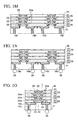
- FIG.1A to FIG.10 are sectional views showing a semiconductor device manufacturing method according to a first embodiment of the present invention.
- FIG.2A to FIG.2E are sectional views showing details of steps in FIG.1K and FIG.1L.
- FIG.1A first a silicon substrate 10 whose thickness is about 400 ⁇ m, for example, is prepared. Then, as shown in FIG.1B, a resist film (not shown) is patterned on the silicon substrate 10 by the photolithography, and then wiring recesses 10a of 3 to 5 ⁇ m depth are formed by dry-etching the silicon substrate 10 while using the resist film as a mask. At this time, areas on which a plurality of semiconductor chips are assembled respectively are defined on the silicon substrate 10 and also a recess 10x used to form an alignment mark is formed at the same time. This recess 10x may be formed near a plurality of semiconductor chip assembling areas respectively or may be formed in the peripheral area of the silicon substrate 10.
- the resist film (not shown) is patterned by the photolithography to open predetermined portions of bottom surfaces of the wiring recesses 10a.
- through holes 10b that are passed through from one surface to the other surface are formed by dry-etching the silicon substrate 10 while using the resist film as a mask. In this manner, the wiring recesses 10a and the through holes 10b that are passed through the wiring recesses 10a are formed on the silicon substrate 10.
- an inorganic insulating film 12 such as a silicon oxide film, or the like is formed on the silicon substrate 10, on which the wiring recesses 10a and the through holes 10b are formed, by the CVD method. Accordingly, inner surfaces of the wiring recesses 10a and the through holes 10b and an upper surface of the silicon substrate 10 are covered with the inorganic insulating film 12.
- This inorganic insulating film 12 is formed to' insulate a conductor, which is buried in the wiring recesses 10a and the through holes 10b by the post process, from the silicon substrate 10.
- a barrier film 14 such as a titanium nitride film (TiN film), a tantalum nitride film (TaN film), or the like is formed on the inorganic insulating film 12 by the sputter method or the CVD method.
- a seed film 16 made of copper is formed on the barrier film 14 by the sputter method or the like.
- the Cu film 18, the seed film 16, and the barrier film 14 are polished by the CMP (Chemical Mechanical Polishing) method until the inorganic insulating film 12 formed on the upper surface of the silicon substrate 10 is exposed. Accordingly, the Cu film 18, the seed film 16, and the barrier film 14 are buried in the through holes 10b and the wiring recesses 10a by the so-called damascene method, so that conductive plugs 18b filled in the through holes 10b and wiring patterns 18a connected to the conductive plugs 18b are formed. At this time, the Cu film 18, the seed film 16, and the barrier film 14 are also buried in the recess 10x for the above alignment mark, and thus an alignment mark 19 is formed at the same time.
- CMP Chemical Mechanical Polishing
- the conductive plugs 18b, the wiring patterns 18a, etc. are formed on the silicon substrate 10 as required, whereby a wiring substrate 11 is obtained.
- the conductive plugs 18b and the wiring patterns 18a connected to the conductive plugs 18b are formed by using the damascene method.
- the silicon substrate in which the conductive plugs are filled in the through holes may be prepared, and then the wiring patterns may be formed by forming the Cu wirings connected to the conductive plugs by means of the so-called additive process or the subtractive process.
- semiconductor chips 20 each including predetermined elements (not shown) such as transistors, or the like, connection pads 21 (connection terminals), and bumps 23 (connection terminals) connected to the connection pad on one surface are prepared.
- the semiconductor chip 20 is formed as the chip by applying the dicing to the semiconductor wafer after predetermined elements, etc. are formed on the semiconductor wafer by the ordinary manufacturing method, and its thickness is about 500 ⁇ m, for example.
- the semiconductor chips 20 prepared herein are the non-defective unit that passes predetermined inspections, and the semiconductor chips as the defective unit are excluded from here.
- the semiconductor chip 20 is exemplified as an example of the electronic chip.
- Various electronic chips such as the silicon chip in which the capacitor element, the resistor, and the like are provided on one surface, etc. may be employed.
- the bumps 23 of the semiconductor chip 20 which is non-defective unit are bonded to the wiring patterns 18a of the wiring substrate 11 by the flip-chip bonding.
- a plurality of semiconductor chips 20 are mounted on a plurality of semiconductor chip mounting areas of the wiring substrate 11 to direct their element non-forming surfaces (referred to as back surfaces hereinafter) the upper side respectively.
- the flip-chip bonding process for example, the solder bump is employed as the bumps 23 of the semiconductor chip 20 and then the bumps 23 of the semiconductor chip 20 and the wiring patterns 18a of the wiring substrate 11 are bonded with the solder.
- the Au bump is employed as the bumps 23 of the semiconductor chip 20 and then the bumps 23 of the semiconductor chip 20 and the wiring patterns 18a of the wiring substrate 11 may be bonded via the anisotropic conductive material (ACF).
- ACF anisotropic conductive material
- an underfill resin 22 is filled in a clearance between the wiring substrate 11 and the semiconductor chip 20.
- an insulating resin NCF or NCP
- NCF insulating resin
- a first insulating film 24 for covering the semiconductor chips 20 is formed on the semiconductor chips 20 and the wiring substrate 11.
- the first insulating film 24 may be formed to expose the back surfaces of the semiconductor chips 20.
- the resin film made of the material that is selected from a group consisting of thermosetting resins including epoxy resin, polyphenylene ether resin, phenol resin, fluororesin, etc. may be employed.
- this resin film is laminated on the semiconductor chips 20 and the wiring substrate 11 at a degree of vacuum of 50 to 1000 Pa and the stage temperature of 50 to 160 °C.
- such resin film is cured by executing the annealing for 10 minute in the oven whose atmosphere is set to 100 °C, so that the resin film is formed. It is preferable that, because the resin film as the first insulating film 24 is ground by the post process, the resin film having still the rigidity after the annealing has been executed should be employed.
- the resin film as the first insulating film 24 may be formed by the spin coating method or the printing method. Also, in addition to the resin film as the first insulating film 24, the silicon oxide film, the silicon nitride film, or the like formed by the CVD method may be employed.
- the semiconductor chips 20 are brought into the condition that they are covered and supported with the first insulating film 24.
- the first insulating film 24 is ground by the grinder to expose the back surfaces of the semiconductor chips 20. Then, a thickness of the semiconductor chips 20 is thinned by grinding simultaneously the semiconductor chips 20 and the first insulating film 24. It is preferable that the grinder whose grinding feed speed can be exchanged in multiple stages should be employed as the grinder used to grind.
- the thickness of semiconductor chips 20 is roughly ground up to about 100 ⁇ m by using the grinding wheel (grindstone) which is formed by binding 20 to 30 ⁇ m diamond particles by the vitrified (glass ceramic) or the resin bond (organic resin).
- the number of revolution of the grindstone spindle is set to about 3000 to 5000 rpm, and the grinding feed speed is reduced to the lower speed as the thickness of the semiconductor chips 20 is reduced smaller (For example, first step (5 to 3 ⁇ m/sec), second step (2 to 0.5 ⁇ m/sec), third step (1 to 0.3 ⁇ m/sec)).
- the finishing grinding is executed by using the grinding wheel (grindstone) which is formed by binding 1 to 10 ⁇ m diamond particles by the vitrified or the resin bond (organic resin) until the thickness of the semiconductor chips 20 is reduced up to about 25 ⁇ m.
- the number of revolution of the grindstone spindle is set to about 3000 to 5000 rpm, and the grinding feed speed is reduced to the lower speed as the thickness of the semiconductor chips 20 is reduced smaller (For example, first step (1 to 0.5 ⁇ m/sec), second step (0.5 to 0.2 ⁇ m/sec), third step (0.2 to 0.05 ⁇ m/sec)).
- the work becomes difficult to contact the binder. Therefore, such an effect (autogenous effect of the diamond) occurs that the grind scraps are dropped away and the fresh diamond is exposed before the diamond of the grindstone causes the clogging. As a result, the clogging of the grindstone can be prevented. Also, it is preferable that the structure in which a foaming rate of the binder of the grindstone is relatively high should be employed. Accordingly, since it can be expected that the grind scraps escape into air pockets of the grindstone, the clogging of the grindstone can be prevented.
- the semiconductor chips 20 and the first insulating film 24 are polished further to about 1 to 5 ⁇ m by the CMP method.
- the grinding surfaces of the semiconductor chips 20 and the first insulating film 24 are planarized as a roughly same surface by the above grinding by means of the grinder. Thus, even if this polishing step is omitted, no trouble is caused.
- the CMP conditions under which polishing rates of the semiconductor chips 20 and the first insulating film (resin film) 24 are set equal to each other should be employed.
- the polishing is carried out by the CMP method using the polyurethane polishing cloth and the slurry in which colloidal silica, cerium oxide, silicon carbide, silicon nitride, iron oxide, or alumina is dispersed into the alkaline aqueous solution such as ammonia, KOH, or the like. Then, the polishing pad and the wiring substrate 11 are rotated at the number of revolution of 200 to 500 rpm respectively, and then the polishing is carried out in the situation that about 1/2 to 2/3 surface out of the area of the wiring substrate 11 contacts the polishing pad.
- the slurry solution is supplied to the polished surface from the inner nozzle, which is arrange on the inside of the polishing pad, and the outer nozzle, which is arrange on the outside of the polishing pad, respectively. According to such configuration, a polishing effect can be improved and also an in-plane uniformity of the polishing can be improved.
- the thickness of the semiconductor chips 20 is thinned to about 20 ⁇ m, for example. It is of course that the final thickness of the semiconductor chips 20 can be adjusted appropriately.
- the semiconductor chips 20 that are divided into individual pieces are mounted on the rigid wiring substrate 11 by the face down flip-chip bonding, then the semiconductor chips 20 are covered and supported with the first insulating film 24, and then the first insulating film 24 and the semiconductor chips 20 are ground to thin the semiconductor chips 20.
- the semiconductor chips 20 that are divided into individual pieces are mounted on the rigid wiring substrate 11 that is also used as the supporting body, then such semiconductor chips 20 are supported with the first insulating film 24, and then the semiconductor chips 20 are ground to reduce the thickness. Therefore, unlike previously-proposed techniques 1 and 2 in which the method of grinding the semiconductor wafer being adhered to the temporary supporting body to reduce the thickness is applied, disadvantages such that the semiconductor wafer is broken, etc. are not generated.
- the non-defective chips are mounted onto the wiring substrate after it is inspected whether or not the semiconductor chips are good. Therefore, unlike previously-proposed technique 3 in which the method of grinding one semiconductor wafer to reduce the thickness is applied after two semiconductor wafers are bonded, there is no possibility that the defective chips are mounted on the wiring substrate 11.
- the semiconductor chips 20 are ground in a state that the semiconductor chips 20 are adhered only via the underfill resin 22, it is possible that the defective bonding is caused between the semiconductor chips 20 and the wiring substrate 11 due to the damage at the time of grinding.
- the semiconductor chips 20 when the semiconductor chips 20 are to be ground, their side surfaces are supported by the first insulating film 24. Therefore, there is no possibility that the bonding between the semiconductor chips 20 and the wiring substrate 11 is damaged during the grinding step, and thus a reduction in the yield of production of the semiconductor device can be prevented.
- the grinding surfaces of the semiconductor chips 20 and the first insulating film 24 can be planarized as the almost same surface. Therefore, as described later, this is convenient for the case where other semiconductor chips are laminated on the semiconductor chips 20 by the flip-chip bonding.
- a method of forming wiring patterns, which are connected to the connection pads 21 on the element non-forming surface side, onto the back surface side of the semiconductor chips 20, as shown in FIG.1H, will be explained hereunder.
- a resist film (not shown) having openings in predetermined portions, which correspond to the connection pads 21 in the peripheral portion on the back surfaces of the thinned semiconductor chips 20, is patterned by the photolithography.
- the alignment can be executed by recognizing the above alignment mark 19 by means of an optical aligning means. Accordingly, the opening portions of the resist film are aligned at predetermined positions with good precision
- the die-by-die alignment system that executes the alignment by recognizing the alignment marks 19, which are formed in vicinity of a plurality semiconductor chip mounting areas respectively, may be employed.
- the global alignment system that executes the alignment by estimating exposure positions in design based on the alignment marks 19, which are formed in the peripheral area of the wiring substrate 11, may be employed.
- the semiconductor chips 20 are etched by the dry etching using the above resist mask as a mask. At this time, the etching of the semiconductor chips 20 is stopped at the connection pads 21 that are formed on the element formation surface. Thus, via holes 20a a depth of which reaches the connection pad 21 on the element formation surface side from the back surface of the semiconductor chip 20 are formed. In this case, the via holes 20a may be formed in the semiconductor chips 20 by using the laser instead of the dry etching.
- the alignment can be executed by recognizing predetermined patterns on the element formation surface side by irradiating the X-rays or the IR (infrared rays) onto the semiconductor chips 20 to transmit therethrough.
- the alignment can be executed by recognizing predetermined patterns on the element formation surface side by irradiating the visible rays onto the semiconductor chips 20 to transmit therethrough.
- the X-rays or the IR (infrared rays) are not used, the necessity of employing the expensive manufacturing system can be eliminated. Thus, reduction in cost of the manufacturing system can be achieved.
- a second insulating film 25 is formed on the semiconductor chips 20 and the first insulating film 24.
- the second insulating film a similar film to the resin film exemplified as the first insulating film 24 may be employed.
- the via holes 20a formed in the semiconductor chips 20 still remain as a cavity.
- an interlayer insulating film 26 consisting of the first insulating film 24 and the second insulating film 25 is formed.
- a resist film (not shown) is patterned on the second insulating film 25 by the photolithography to open predetermined areas including the via hole 20a portions of the semiconductor chips 20. Then, the second insulating film 25 is etched by using the resist film as a mask. Thus, the via holes 20a are exposed again and also wiring recesses 25a that are communicated with the via holes 20a are formed.
- a resin film may be formed by coating a resin on the semiconductor chips 20 and the first insulating film 24 in place of the adhesion of the insulating film and then applying the annealing to the resin to cure it.
- the resin film since the resin film is filled in the via holes 20a, such resin film filled in the via holes 20a is removed by the step of forming the wiring recesses 25a.
- FIG.2A to FIG.2E are partially enlarged views showing an A portion in FIG.1K in an enlarged manner.
- an inorganic insulating film 28 such as a silicon oxide film or the like is formed on inner surfaces of the via holes 20a and the wiring recesses 25a and an upper surface of the second insulating film 25 in FIG.2A by the CVD method.
- This inorganic insulating film 28 is formed to insulate a conductor, which is filled in the via holes 20a and the wiring recesses 25a, from the semiconductor chips 20.
- the inorganic insulating film 28 formed on bottom portions of the via holes 20a is removed selectively by the laser, or the like.
- the connection pads 21 are exposed from the bottom portions of the via holes 20a.
- a barrier film 30 made of a TiN film, a TaN film, or the like is formed on the resultant structure in FIG.2C, and then a seed film 32 made of a Cu film is formed. Then, a Cu film 34 having a film thickness that buries the via holes 20a and the wiring recesses 25a is formed on the seed film 32 by the electroplating using the seed film 32 and the barrier film 30 as a plating power-supply layer.
- the Cu film 34, the seed film 32, and the barrier film 30 are polished by the CMP method until an upper surface of the inorganic insulating film 28 is exposed.
- the barrier film 30, the seed film 32, and the Cu film 34 are buried in the via holes 20a and the wiring recesses 25a, so that a conductive plug 34b and a wiring pattern 34a (conductive film pattern) connected to the conductive plug 34b are formed.
- the conductive plug 34b and the wiring pattern 34a may be formed by coating a conductive paste in the via holes 20a and the wiring recesses 25a to bury them, and then polishing the conductive paste by the CMP method.
- connection pad 21 on the element formation surface of the semiconductor chip 20 is connected electrically to the wiring pattern 34a on the back surface side via the conductive plug 34b filled in the via hole 20a.
- FIG.1F a series of steps from the step of bonding the semiconductor chips 20 by the flip-chip bonding (FIG.1F) to the step of forming the wiring patterns 34a on the back surface side of the semiconductor chips 20 (FIG.1L) are repeated n times (n is an integer of 1 or more).
- n is an integer of 1 or more.
- the uppermost semiconductor chips 20 are mounted by the flip-chip mounting, and then the first insulating film 24 is formed and then polished.
- FIG.1M shows the mode that four semiconductor chips 20 are laminated and packaged.
- a passivation film 36 made of the silicon nitride film, the polyimide film, or the like is formed on the uppermost semiconductor chips 20 and the first insulating film 24. Since the above interlayer insulating film 26 consisting of the first insulating film 24 and the second insulating film 25 is formed of the resin films, for example, such interlayer insulating film 26 is formed in the situation that the residual stress of the film is relatively large. In addition, since the interlayer insulating film 26 made of the resin film are laminated and formed, it is supposed that a bowing is generated in the resultant structure in FIG.1M due to the residual stress of these films.
- the bowing can be corrected by forming the passivation film 36 when the bowing is generated in the resultant structure in FIG.1M.
- the passivation film 36 is formed to apply the compressive stress that cancels the tensile stress of the interlayer insulating film 26.
- bumps 38 are formed by mounting solder balls on the conductive plugs 18b that are exposed from the surface of the wiring substrate 11, on which the semiconductor chips 20 are not mounted.
- the thickness of the wiring substrate 11 may be thinned up to about 50 to 100 ⁇ m by polishing the surface of the wiring substrate 11, on which the semiconductor chips 20 are not mounted, prior to the formation of the bumps 38.
- the structural body (stacked CSP structure) in which a plurality of semiconductor chips 20 are laminated and packaged is arranged successively on plural areas of the wiring substrate 11.
- a semiconductor device 1 having the stacked CSP structure according to the present embodiment is completed by dividing a plurality of structural bodies in FIG.1N individually.
- the bumps 38 may be formed after a plurality of structural bodies in FIG.1M are divided.
- a plurality of structural bodies may be divided to include two stacked CSP structures or more.
- the semiconductor chips 20 are mounted on the wiring substrate 11 by the flip-chip mounting, and also the back surfaces of the semiconductor chips 20 are ground to reduce the thickness in a state that the semiconductor chips 20 are held by the first insulating film 24.
- the wiring patterns 34a are formed on the back surface side of the semiconductor chips 20, and also the wiring patterns 34a are connected electrically to the connection pads 21 on the element formation surface via the via holes 20a that pass through the semiconductor chips 20.
- a plurality of semiconductor chips 20 having such structure are laminated three-dimensionally, connected mutually and packaged in the state that the semiconductor chips 20 are buried in the interlayer insulating film 26.
- the packaging structure in which parent chips and child chips are laminated on the wiring substrate in a face-up fashion and packaged and also the connection pads of these chips are connected to the wiring substrate by the wire bonding method is supposed.
- the child chips are mounted in a state that wire bonding areas of the parent chips are assured, a size of the child chip is restricted.
- a plurality of semiconductor chips 20 are bonded mutually via the via holes 20a formed in the semiconductor chips 20 and connected electrically to the wiring substrate 11.
- a plurality of semiconductor chips 20 having any size can be arranged and laminated without limitation of their mutual sizes.
- selection of the semiconductor chips to be mounted can be expanded, and thus a margin in design can be improved.
- the wiring patterns 34a are formed on the back surfaces of the semiconductor chips 20 via the thin inorganic insulating film 28, the thickness of the semiconductor device 1 in which a plurality of semiconductor chips 20 are packaged can be reduced.
- the upper and lower semiconductor chips 20 are connected mutually by the wirings provided in the vertical direction via the via holes 20a that pass through the semiconductor chips 20. Therefore, a wiring length can be shortened rather than the case where the semiconductor chips are connected by the bonding wires or the case where the wirings containing the wiring routing in the lateral direction are implemented. As a result, the semiconductor device can respond to a higher speed of the signal speed in the high frequency application.
- the wiring length can be shortened. Therefore, this is convenient for a viewpoint that the performance of the semiconductor device 1 can be improved.
- the semiconductor chips 20 that are divided into the individual pieces are polished to reduce the thickness in the state that they are held by the first insulating film 24 after they are mounted on the wiring substrate 11 by the flip-chip mounting. Therefore, no handling of the thinned semiconductor chips 20 that are difficult to handle is needed. If doing this, the thickness of the semiconductor chips 20 can be reduced up to about 10 ⁇ m not to generate any disadvantage.
- the first insulating film 24 is also ground at the same time when the semiconductor chips 20 are ground. Therefore, both grinding surfaces of semiconductor chips 20 whose thickness is thinned and the first insulating film 24 can be planarized to have an almost same height.
- the mode that the bumps 23 of the semiconductor chips 20 are bonded and mounted is exemplified. Since the mounting surfaces are planarized as described above, the connection pads 21 of the overlying semiconductor chips 20 can be directly bonded to the wiring patterns 34a on the back surface side of the underlying semiconductor chips 20 without intervention of the bumps 23 to mount. In addition, since the wiring patterns 18a of the wiring substrate 11 are formed by the damascene method, the mounting surface of the wiring substrate 11 are also planarized. Therefore, the bumps 23 can be omitted similarly from the lowermost semiconductor chips 20 that are bonded to the wiring substrate 11.
- the thickness of the semiconductor device 1 can be further reduced.
- the mode that a plurality of laminated semiconductor chips 20 are connected mutually via the via holes 20a formed in these semiconductor chips 20 is exemplified.
- a plurality of semiconductor chips 20 may be connected mutually via the via holes that are formed in the first insulating film 24 in the neighborhood of the semiconductor chips.
- the semiconductor device according to the first embodiment may be manufactured by using the glass substrate in place of the silicon substrate 10. In this case, it is not needed to form the inorganic insulating film 12.
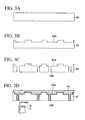
- FIG.3A to FIG.30 are sectional views showing a semiconductor device manufacturing method according to a second embodiment of the present invention in order of steps.
- Different points of the second embodiment from the first embodiment reside in that the wiring substrate is formed of an insulating substrate and that a plurality of laminated semiconductor chips are connected mutually via the via holes that are formed in the insulating film in the neighborhood of the semiconductor chips.
- detailed explanations of the steps that are similar to the first embodiment will be omitted herein.
- an insulating substrate 40 is prepared.
- a substrate selected from a group consisting of a resin substrate made of FR4, BT or the like, a glass substrate, a ceramic substrate, a sapphire substrate, etc. may be employed.
- wiring recesses 40a are formed on the insulating substrate 40, and then through holes 40b that pass from predetermined areas of bottom surfaces of the wiring recesses 40a to the back surface are formed.
- the barrier film 14 and the seed film 16 are formed sequentially on the insulating substrate 40, in which the wiring recesses 40a and the through holes 40b are formed, by the same method as the first embodiment.
- the Cu film 18 is formed by the electroplating to have a film thickness that can bury the wiring recesses 40a and the through holes 40b. In this case, since the insulating substrate 40 is employed in the second embodiment, it is not needed to form the inorganic insulating film before the barrier film 14 is formed.
- the Cu film 18, the seed film 16, and the barrier film 14 are polished by the CMP method until an upper surface of the insulating substrate 40 is exposed. Accordingly, the conductive plugs 18b, which are filled in the through holes 40b, and the wiring pattern 18a, which are connected to the conductive plugs 18b, are formed, and thus a wiring substrate 11a is obtained.
- the mode that the conductive plugs 18b filled in the through holes 40b and the wiring pattern 18a connected to the conductive plugs 18b are formed by using the damascene method is exemplified.
- a base substrate for the built-up wiring in which the through-hole Cu plating layer is formed and the holes are filled with the resin
- Cu wirings connected to the through-hole Cu plating layer may be formed by the so-called additive method or the subtractive method to form wiring patterns.
- the first insulating film 24 is formed on the wiring substrate 11a to have a film thickness that exposes at least the back surfaces of the semiconductor chips 20.
- first a coating liquid such as an epoxy resin or a polyimide resin is dropped on a center portion of the wiring substrate 11a by a predetermined amount while rotating the wiring substrate 11a at a low speed of about 300 rpm.
- the coating liquid is spread over an overall surface of the wiring substrate 11a.
- the coating film formed to spread over the back surface of the wiring substrate 11a is excluded by rotating the wiring substrate 11a at a high speed of about 3000 rpm.
- the coating film having a thickness that exposes the back surfaces of the semiconductor chips 20 is formed on the mounting surface of the wiring substrate 11a.
- the coating film is cured by annealing in an oven whose atmosphere is set to 150 °C,so that a resin film is formed.
- the first insulating film 24 made of the resin film in a so-called fillet form is formed between a plurality of semiconductor chips 20 in the state that the back surfaces of the semiconductor chips 20 are exposed.
- the semiconductor chips 20 are supported by the first insulating film 24 in this manner.
- the thickness of the semiconductor chips 20 is thinned to about 20 ⁇ m by grinding the semiconductor chips 20 and the first insulating film 24 by virtue of the grinder.
- the semiconductor chips 20 may be polished by the CMP method after such semiconductor chips 20 are ground by the grinder.
- via holes 24a are formed by opening the portions, which correspond to predetermined portions of the wiring patterns 18a on the wiring substrate 11 in the first insulating film 24 in the neighborhood of the semiconductor chips 20, by the laser.
- photosensitive polyimide resin may be employed as the first insulating film 24 and then the via holes 24a may be formed by exposing/developing the resin.
- the second insulating film 25 is formed on the first insulating film 24 and the semiconductor chips 20.
- the interlayer insulating film 26 consisting of the first insulating film 24 and the second insulating film 25 is formed.
- the wiring recesses 25a are formed by etching predetermined areas including the portions that correspond to the via holes 24a in the second insulating film 25.
- the via holes 24a and the wiring recesses 25a, which are communicated with the via holes 24a are formed.
- a resin layer which is formed by a spin coating method or a printing method may be employed instead of the resin film.
- the barrier film, the seed film, and the Cu film are formed sequentially from the bottom on the resultant structure in FIG.3K.
- the conductive plugs 34b and the wiring patterns 34a connected to the conductive plugs 34b are formed by polishing these layers.
- the wiring patterns 18a of the wiring substrate 11 are connected electrically to the wiring patterns 34a formed on the back surface side of the semiconductor chips 20 via the conductive plugs 34b.
- a series of steps from the step of bonding the semiconductor chips 20 to the wiring substrate 11 by the flip-chip bonding (FIG.3F) to the step of forming the wiring patterns 34a on the back surface side of the semiconductor chips 20 (FIG.3L) are repeated n times (n is an integer of 1 or more). Then, the uppermost semiconductor chips 20 are mounted by the flip-chip mounting, and then the first insulating film 24 is formed and then polished.
- the passivation film 36 is formed on the second insulating film 25 to serve also as the purpose of correcting the bowing of the resultant structure in FIG.3M.
- a semiconductor device 1a having the stacked CSP structure is completed by dividing a plurality of structural bodies in FIG.3N individually.
- the via holes 20a that pass through the semiconductor chips are not formed in a plurality of semiconductor chips 20, but the via holes 24a are formed in the first insulating film 24 in vicinity of a plurality of semiconductor chips 20 respectively.
- the lowermost semiconductor chips 20 are mounted on the wiring patterns 18a of the wiring substrate 11 by the flip-chip mounting, and the back surfaces of the semiconductor chips 20 are ground and thinned in the state that such semiconductor chips 20 are held by the first insulating film 24.
- the wiring patterns 34a are formed on the back surfaces of the semiconductor chips 20 to contact them.
- the wiring patterns 34a are connected electrically to the connection pads 21 on the element formation surface side via the via holes 24a formed in the first insulating film 24.
- a plurality of semiconductor chips 20 having such structure are laminated three-dimensionally and connected mutually in the state that the semiconductor chips 20 are buried in the interlayer insulating film 26.
- the semiconductor device 1a of the second embodiment can achieve the same advantages as the first embodiment.
- the wiring patterns are formed in the state that they come into contact with the back surfaces of the semiconductor chips 20. Therefore, the thickness of the semiconductor device 1 in which a plurality of semiconductor chips 20 are packaged can be further thinned.
- the via holes 20a are not formed in the semiconductor chips 20, but the via holes 24a are formed in the first insulating film 24. Therefore, the via holes 24a can be formed easily by employing the laser equipment and the exposure equipment, which are normally used, without the introduction of the special aligning means. As a result, a production cost of the semiconductor device can be reduced lower than the first embodiment.
- the wiring substrate 11 may be formed by using the insulating substrate 40, and also a plurality of semiconductor chips may be connected mutually not by forming the via holes 24a in the first insulating film 24 but by forming the via holes 20a in the semiconductor chips 20, like the first embodiment.
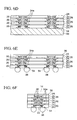
- FIG.4A to FIG.4C are sectional views showing a semiconductor device manufacturing method according to a third embodiment of the present invention.
- the resin substrate made of FR4, BT, or the like is employed particularly as the insulating substrate, the resin substrate is inferior in the fine patterning characteristic to the silicon substrate. Therefore, such a situation is supposed that an increase in the production cost is brought about in the step of forming the fine wiring recesses and the through via holes by the damascene method.
- the third embodiment can overcome such disadvantage. In this case, detailed explanation of the same steps as the first and second embodiments will be omitted herein.
- a wiring substrate 11b in which the predetermined wiring patterns 18a made of the Cu wiring are formed on one surface of the insulating substrate 40 is formed.
- a photosensitive insulating resin film pattern having opening portions, at which the wiring patterns 18a of the insulating substrate 40 are formed, is formed, and then the Cu film is formed selectively in the opening portions by the electroless plating (additive method). Otherwise, the Cu film is formed on one surface of the insulating substrate 40 by the electroless plating and electroplating, and then the Cu film is patterned by the photolithography and the etching (subtractive method).
- the wiring patterns 18a are formed on the insulating substrate 40 by the normal additive method or subtractive method. Therefore, the step of forming the wiring recesses and the through via holes by finely patterning the insulating substrate 40 is not needed, and thus an increase in the production cost of the wiring substrate can be suppressed.
- a plurality of semiconductor chips 20 connected to the wiring patterns 18a of the wiring substrate 11b are laminated and packaged.
- the passivation film 36 is formed on the second insulating film 25 on the uppermost semiconductor chips 20. Then, the interlayer insulating film 26 and the passivation film 36 laminated on the outside portion of the wiring patterns 18a of the wiring substrate 11b are etched by the drill, the laser, or the like. Thus, via holes 42 for exposing a part of the wiring patterns 18a of the wiring substrate 11b are formed.
- conductive plugs 44 connected to the wiring patterns 18a of the wiring substrate 11b are formed by filling the conductive paste in the via holes 42, or the like. Then, the bumps 38 connected to the conductive plugs 44 are formed.
- a semiconductor device 1b having the stacked CSP structure is completed by dividing a plurality of structural bodies in FIG.4B individually.
- a plurality of semiconductor chips 20 are connected mutually and laminated on the wiring substrate 11b to have the same structure as the second embodiment.
- the wiring patterns 18a of the wiring substrate 11b are connected to the bumps 38 formed on the surface on passivation film 36 side via the via holes 42 formed in the laminated interlayer insulating films 26.
- the third embodiment can achieve the same advantages as the second embodiment.
- the semiconductor device according to the third embodiment of the present invention can be manufactured easily without the increase in the production cost even when the resin substrate that is inferior in the fine patterning characteristic to the silicon substrate is employed.
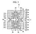
- FIG.5 is a sectional view showing a semiconductor device manufacturing method according to a fourth embodiment of the present invention.
- the fourth embodiment provides the mode that a plurality of semiconductor chips are laminated on both surfaces of the wiring substrate and packaged respectively.
- the same reference numbers are affixed to the same elements as those in FIG.30, and their detailed explanation will be omitted herein.
- a semiconductor device 1c of the fourth embodiment shows the mode that a plurality of semiconductor chips are also laminated on the back surface (surface on which the bumps 38 are mounted) side of the wiring substrate 11 in the semiconductor device 1a of the second embodiment (FIG.30).
- wiring patterns 18c are also formed on the back surface side of the wiring substrate 11 of the fourth embodiment. These wiring patterns 18c are connected electrically to the wiring patterns 18a on the surface side via the conductive plugs 18b that are filled in the through holes 10b of the wiring substrate 11.
- the bumps 23 of the semiconductor chips 20 are bonded to the wiring patterns 18c on back surface side by the flip-chip bonding.
- the wiring patterns 34a are formed on the back surface side of the semiconductor chips 20. These wiring patterns 34a are connected electrically to the connection pads 21 on the element formation surface side via the via holes 24a formed in the first insulating film 24.
- a plurality of semiconductor chips 20 having such structure are laminated three-dimensionally and connected mutually in the state that the semiconductor chips 20 are buried in the interlayer insulating film 26.
- the packaging density can be improved higher than the first to third embodiments.
- the mode in which a plurality of semiconductor chips 20 are laminated on both surfaces of the wiring substrate 11 by applying the packaging method of the second embodiment is shown, the mode in which a plurality of semiconductor chips 20 are laminated on both surfaces of the wiring substrate 11 by applying the packaging method of the first embodiment may be employed.
- such a mode may be employed that, in the semiconductor device 1b of the third embodiment (FIG.4C), the substrate, the wiring patterns formed on both surfaces of which are connected mutually via the through holes, is employed as the wiring substrate 11b, and that a plurality of semiconductor chips 20 connected electrically to the wiring patterns are laminated on the surface of the wiring substrate 11b on which the semiconductor chips 20 are not mounted.
- FIG.6A to FIG.6F are sectional views showing a semiconductor device manufacturing method according to a fifth embodiment of the present invention.
- the fifth embodiment provides the mode that a metal plate having predetermined wiring patterns (connection pads) thereon is employed as the wiring substrate and that a plurality of semiconductor chips connected to the wiring patterns of the metal plate are laminated and packaged by applying the packaging method of the first or second embodiment and then only the metal plate is removed selectively.
- connection pads connection pads
- a metal plate 50 made of copper, or the like is prepared. Then, a resist film 52 having opening portions 52a at portions, on which the wiring patterns are formed, is formed on one surface of the metal plate 50 by the photolithography. At this time, the other surface of the metal plate 50 is covered with the resist film 52.
- a gold layer 54a, a nickel layer 54b, and a gold layer 54c are formed sequentially in the opening portions 52a by the electroplating using the metal plate 50 as the plating power-supply layer while using the resist film 52 as a mask. Then, the resist film 52 is removed.
- wiring patterns (connection pads) 54 each consisting of the gold layer 54a, the nickel layer 54b, and the gold layer 54c are formed on the metal plate 50.
- a plurality of semiconductor chips 20 connected electrically to the wiring patterns 54 on the metal plate 50 are packaged.
- the semiconductor chips 20 may be packaged by using the packaging method of the second embodiment.
- the passivation film 36 for covering the uppermost semiconductor chips 20 is formed.
- the metal plate 50 is selectively etched with respect to the wiring patterns 54 and the first insulating film 24 and removed.
- the metal plate 50 can be etched selectively with respect to the wiring patterns (gold layer/nickel layer/gold layer) 54 and the first insulating film (resin film) 24 by the wet etching using an iron (III) chloride aqueous solution, a copper (II) chloride aqueous solution, an ammonium peroxide aqueous solution, or the like and can be removed.
- the wiring patterns 54 connected to the semiconductor chips 20 are exposed from the lower surface of the first insulating film 24.
- a semiconductor device 1d of the fifth embodiment having the stacked CSP structure is completed by dividing a plurality of structural bodies in FIG.6E individually.
- the bumps 23 of the lowermost semiconductor chips 20 out of a plurality of laminated semiconductor chips 20 are bonded to the upper surfaces of the wiring patterns 54, the lower surfaces of which are connected to the bumps 38 and which are buried in the first insulating film 24, by the flip-chip bonding.
- the semiconductor chips 20 except the lowermost semiconductor chips 20 are bonded to the wiring patterns 34a, which are formed on the back surface side of the underlying semiconductor chips 20 respectively, by the flip-chip bonding.
- a plurality of semiconductor chips 20 that are laminated three-dimensionally are connected mutually via the via holes 20a formed in the semiconductor chips 20.
- the semiconductor device 1d of the fifth embodiment can achieve the same advantages as the first embodiment. Also, since the wiring substrate is not provided, the thickness of the semiconductor device can be reduced correspondingly thinner than the semiconductor device having the wiring substrate in other embodiments.
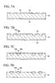
- FIG.7A to FIG.7G are sectional views showing a semiconductor device manufacturing method according to a sixth embodiment of the present invention.
- Different points of the sixth embodiment from the fifth embodiment reside in that not only the wiring patterns are formed on the metal plate but also the bumps connected to the wiring patterns are formed in advance in the metal plate. In this case, detailed explanations of the same elements and the same steps as those in other embodiments will be omitted herein.
- the resist film 52 having the opening portions 52a used to form the wiring patterns on one surface of the metal plate 50 made of copper is patterned, and the other surface is covered with the resist film 52.
- concave portions 50a are formed by etching the exposed portions of the metal plate 50 while using the resist film 52 as a mask. Then, the solder plating is applied to inner portions of the concave portions 50a on the metal plate 50 by the electroplating using the metal plate 50 as the plating power-supply layer, while using the resist film 52 as a mask. Thus, solder layers 38a are formed.
- the wiring patterns 54 made of the laminated film (gold layer/nickel layer/gold layer) similar to the fifth embodiment are formed in the opening portions 52a in the resist film 52.
- the resist film 52 is removed.
- the solder layers 38a are filled in the concave portions 50a on the metal plate 50, so that the wiring patterns 54 formed and connected to the solder layers 38a are obtained.
- the solder layers 38a are formed as the bumps by the post steps.
- the packaging method similar to the first embodiment a plurality of semiconductor chips 20 connected electrically to the wiring patterns 54 on the metal plate 50 are packaged.
- the semiconductor chips 20 may be packaged by applying the packaging method similar to the second embodiment.
- the passivation film 36 for covering the uppermost semiconductor chips 20 is formed.
- the metal plate 50 is selectively etched with respect to the solder layers 38a and the first insulating film 24 and removed.
- the metal plate 50 is formed of copper, the metal plate 50 can be removed selectively with respect to the solder layers 38a and the first insulating film (resin film) 24 by using the wet etchant similar to the fifth embodiment. As a result, the solder layers 38a are exposed to act as the bumps 38.
- FIG.7G like the first embodiment, a semiconductor device 1e of the sixth embodiment having the stacked CSP structure is completed by dividing a plurality of structural bodies in FIG.7F individually.
- the sixth embodiment can achieve the same advantages as the first embodiment. Also, since the wiring substrate is not provided like the fifth embodiment, the thickness of the semiconductor device can be reduced rather than other embodiments.
- the mode that the wiring patterns 18a of the wiring substrate 11 made of the silicon substrate 10 are connected to the bumps 38 mounted on the passivation film 36 side via the via holes formed in the interlayer insulating film 26 may be employed.
Landscapes
- Internal Circuitry In Semiconductor Integrated Circuit Devices (AREA)
- Mechanical Treatment Of Semiconductor (AREA)
Abstract
Description
Therefore, no handling of the thinned semiconductor chips that are difficult to handle is needed.
Claims (23)
- A semiconductor device manufacturing method comprising the steps of:preparing a wiring substrate (11) including a wiring pattern (18a) on a surface;bonding a connection terminal (23) of an electronic chip (20), which has a predetermined element and the connection terminal (23) on one surface, to the wiring pattern (18a) of the wiring substrate 11 by a flip-chip bonding;forming a first insulating film (24) on the wiring substrate (11),the first insulating film having a film thickness that covers the electronic chip (20), or a film thickness that exposes at least another surface of the electronic chip (20); andreducing a thickness of the electronic chip (20) by grinding the first insulating film (24) and another surface of the electronic chip (20).
- A semiconductor device manufacturing method according to claim 1, wherein the step of reducing a thickness of the electronic chip (20) is the step of grinding by a grinder, or the step of grinding by the grinder and then polishing by CMP.
- A semiconductor device manufacturing method according to claim 1 or 2, wherein, in the step of reducing a thickness of the electronic chip (20), a grinding surface of the electronic chip (20) and an upper surface of the first insulating film (24) are planarized at an almost same height.
- A semiconductor device manufacturing method according to any preceding claim, after the step of reducing a thickness of the electronic chip (20), further comprising the steps of:forming a via hole (20a) having a depth, which reaches the connection terminal (23) on one surface of the electronic chip (20) from a predetermined portion on another surface of the electronic chip (20), in the electronic chip (20);forming a second insulating film 25 on the electronic chip (20) and the first insulating film (24);forming a wiring recess (25a), which communicates with the via hole (20a), by etching a predetermined portion of the second insulating film (25) containing a portion that corresponds to the via hole (20a); andforming a conductive film pattern (34a), which is electrically connected to the connection terminal (23) via the via hole (20a), by filling a conductive film in the via hole (20a) and the wiring recess (25a).
- A semiconductor device manufacturing method according to claim 4, after the step of forming the conductive film pattern 34a, further comprising the step of:laminating three-dimensionally and packaging a plurality of electronic chips (20) on the wiring substrate (11), based on n-times (n is an integer of 1 or more) repetition of a series of steps from the step of bonding the electronic chip (20) by the flip-chip bonding to the step of forming the conductive film pattern (34a) connected to the connection terminal (23) via the via hole (20a).
- A semiconductor device manufacturing method according to claim 4 or 5, wherein the wiring substrate (11) has an alignment mark (19) that is formed simultaneously with the conductive film pattern (34a), and
a portion in which the via hole (20a) of the electronic chip (20) is formed is identified based on recognition of the alignment mark (19), in the step of forming the via hole (20a) in the electronic chip (20). - A semiconductor device manufacturing method according to any one of claims 4 to 6, wherein, in the step of forming the via hole (20a) in the electronic chip (20), a portion in which the via hole (20a) of the electronic chip (20) is formed is identified based on recognition of a predetermined pattern on one surface of the electronic chip (20) executed by irradiating X-rays, infrared rays or visible rays from another surface of the electronic chip (20) to transmit therethrough.
- A semiconductor device manufacturing method according to any one of claims 1 to 3, after the step of reducing a thickness of the electronic chip (20), further comprising the steps of:forming a via hole (24a) having a depth, which reaches the wiring pattern (18a) of the wiring substrate 11 from an upper surface of a predetermined portion of the first insulating film (24), in the first insulating film (24);forming a second insulating film (25) on the electronic chip (20) and the first insulating film (24);forming a wiring recess (25a), which communicates with the via hole (24a), by etching a predetermined portion of the second insulating film (25) containing a portion that corresponds to the via hole (24a); andforming a conductive film pattern (34a), which is connected to the wiring pattern (18a) of the wiring substrate (11) via the via hole (24a), by filling a conductive film in the via hole (24a) and the wiring recess (25a).
- A semiconductor device manufacturing method according to claim 8, after the step of forming the conductive film pattern (34a), further comprising the step of:laminating three-dimensionally and packaging a plurality of electronic chips (20) on the wiring substrate (11), based on n-times (n is an integer of 1 or more) repetition of a series of steps from the step of bonding the electronic chip (20) by the flip-chip bonding to the step of forming the conductive film pattern (34a) connected to the wiring pattern (18a) of the wiring substrate (11) via the via hole (24a).
- A semiconductor device manufacturing method according to any one claims 5 to 7, and 9, after the step of laminating three-dimensionally and packaging a plurality of electronic chips (20) on the wiring substrate (11), further comprising the step of:forming a passsivation film (36) on or over uppermost electronic chip (20) in the plurality of electronic chips (20).
- A semiconductor device manufacturing method according to claim 10, wherein a conductive plug (18b) that is connected to the wiring pattern (18a) and filled in a through hole (10b) which passes through the wiring substrate (11), is formed in the wiring substrate (11), and
after the step of laminating three-dimensionally and packaging a plurality of electronic chips (20) on the wiring substrate 11, further comprising the step of:forming a bump (38) that is connected to the conductive plug (18b) exposed from an opposite surface of the wiring substrate (11) to a surface on which the wiring pattern (18a) is formed. - A semiconductor device manufacturing method according to claim 10, after the step of forming the passsivation film (36), further comprising the steps of:forming a via hole (42) that exposes a part of the wiring pattern (18a), by etching a plurality of interlayer insulating films (26) each consisting of the first insulating film (24) and the second insulating film (25), and the passsivation film (36), on an area which is over the wiring pattern (18a)and on the area on which the electronic chip (20) is not mounted;forming a conductive plug (44) in the via hole (42); andforming a bump (38) connected to the conductive plug (44).
- A semiconductor device manufacturing method according to claim 10, wherein the wiring substrate (11) is a metal plate (50) including the wiring pattern (54) on a surface, and
after the step of forming the passsivation film (36), further comprising the steps of:exposing the wiring pattern (54) by selectively etching the metal plate (50) with respect to the wiring pattern (54) and the first insulating film (24) thereby to remove the metal plate (50); andforming a bump (38) connected to the wiring pattern (54). - A semiconductor device manufacturing method according to claim 10, wherein the wiring substrate (11) is a metal plate (50) including a solder layer (38a) filled in concave portions (50a) provided to the metal plate (50), and the wiring pattern (54) formed on the solder layer (38a), and
after the step of forming the passsivation film (36), further comprising the step of:forming a bump (38), by selectively etching the metal plate (50) with respect to the solder layer (38a) and the first insulating film (24) thereby to remove the metal plate (50) and to expose the solder layer (38a). - A semiconductor device manufacturing method according to any one of claims 11 to 14, wherein a structural body in which the electronic chip (20) is laminated and packaged is formed in plural areas of the wiring substrate (11), and
before or after the step of forming the bump (38), further comprising the step of:dividing the wiring substrate (11) such that the structural body in which the electronic chip (20) is laminated and packaged is contained by a predetermined number. - A semiconductor device manufacturing method according to any preceding claim, wherein, in the step of reducing a thickness of the electronic chip (20), the thickness of the electronic chip (20) is about 150 µm or less.
- A semiconductor device, in which a plurality of electronic chips (20) which include a predetermined element and a connection terminal (23),on one surface of the electronic chip (20), and a conductive film pattern (34a) that is connected electrically to the connection terminal (23) via a via hole (20a) which passes through the electronic chip (20), on another surface side of the electronic chip (20), are laminated and packaged on a wiring substrate (11) including a wiring pattern (18a), in a direction that is perpendicular to a surface direction of the wiring substrate (11), in a state that the electronic chips (20) are buried in an interlayer insulating film (26),
wherein a thickness of the electronic chips (20) is about 150 µm or less, and the connection terminals (23) of the electronic chips (20) are bonded to the wiring pattern (18a) of the underlying wiring substrate (11) or the conductive film pattern (34a) of the electronic chip (20) by a flip-chip bonding respectively, and the plurality of electronic chips (20) are connected mutually via the via holes (20a) in the electronic chips (20). - A semiconductor device according to claim 17, further comprising:a passivation film (36) formed on or over uppermost electronic chip (20) in the plurality of electronic chips (20).
- A semiconductor device according to claim 17 or 18, wherein a bump (38) connected to the wiring pattern (18a) via a through hole (10b) which passes through the wiring substrate (11), is provided on an opposite surface of the wiring substrate (11) to a surface on which the wiring pattern (18a) is formed.
- A semiconductor device according to claim 18, wherein a bump (38) connected electrically to the wiring pattern (18a) of the wiring substrate (11) via a via hole (42) which is formed in the interlayer insulating film (26) and the passivation film (36) on an area which is over the wiring pattern (18a) and on the area on which the electronic chip (20) is not mounted, is provided to a surface of the semiconductor device on which the passivation film (36) is formed.
- A semiconductor device, in which a plurality of electronic chips (20) which include a predetermined element and a connection terminal (23), on one surface of the electronic chip (20), and a conductive film pattern (34a) which is connected electrically to the connection terminal (23) via a via hole (20a) which passes through the electronic chip (20), on another surface side of the electronic chip (20), are laminated three-dimensionally and packaged in a state that the electronic chips (20) are buried in an insulating film (26),
wherein a thickness of the electronic chip (20) is about 150 µm or less, and the connection terminal (23) of the lowermost electronic chip (20) in the plurality of electronic chips (20) is bonded to the upper surface of a wiring pattern (54) which is buried in an insulating film (26) in a state that the lower surface of the wiring pattern is exposed, by a flip-chip bonding, and the connection terminals (23) of other electronic chips (20) in the plurality of electronic chips (20) are bonded to the conductive film pattern (34a) of the underlying electronic chip (20) by the flip-chip bonding respectively, whereby the plurality of electronic chips (20) are connected mutually via the via holes (20a) in the electronic chips (20). - A semiconductor device according to claim 21, wherein a bump (38) is connected to lower surface of the wiring pattern (54) to which the connection terminal (23) of the lowermost electronic chip (20) is bonded.
- A semiconductor device according to any one of claims 17 to 22, wherein the conductive film pattern (34a) formed on another surface side of the electronic chip (20) is formed to come into contact with another surface of the electronic chip (20).
Priority Applications (1)
| Application Number | Priority Date | Filing Date | Title |
|---|---|---|---|
| EP06124616A EP1801866B1 (en) | 2002-11-05 | 2003-11-05 | Method of manufacturing a semiconductor device |
Applications Claiming Priority (2)
| Application Number | Priority Date | Filing Date | Title |
|---|---|---|---|
| JP2002320980A JP4056854B2 (en) | 2002-11-05 | 2002-11-05 | Manufacturing method of semiconductor device |
| JP2002320980 | 2002-11-05 |
Related Child Applications (1)
| Application Number | Title | Priority Date | Filing Date |
|---|---|---|---|
| EP06124616A Division EP1801866B1 (en) | 2002-11-05 | 2003-11-05 | Method of manufacturing a semiconductor device |
Publications (3)
| Publication Number | Publication Date |
|---|---|
| EP1418617A2 true EP1418617A2 (en) | 2004-05-12 |
| EP1418617A3 EP1418617A3 (en) | 2004-05-26 |
| EP1418617B1 EP1418617B1 (en) | 2008-10-29 |
Family
ID=32105417
Family Applications (2)
| Application Number | Title | Priority Date | Filing Date |
|---|---|---|---|
| EP03256994A Expired - Lifetime EP1418617B1 (en) | 2002-11-05 | 2003-11-05 | Semiconductor device and method of manufacturing the same |
| EP06124616A Expired - Lifetime EP1801866B1 (en) | 2002-11-05 | 2003-11-05 | Method of manufacturing a semiconductor device |
Family Applications After (1)
| Application Number | Title | Priority Date | Filing Date |
|---|---|---|---|
| EP06124616A Expired - Lifetime EP1801866B1 (en) | 2002-11-05 | 2003-11-05 | Method of manufacturing a semiconductor device |
Country Status (7)
| Country | Link |
|---|---|
| US (2) | US6958544B2 (en) |
| EP (2) | EP1418617B1 (en) |
| JP (1) | JP4056854B2 (en) |
| KR (1) | KR20040040352A (en) |
| CN (1) | CN1499590A (en) |
| DE (2) | DE60324376D1 (en) |
| TW (1) | TW200414495A (en) |
Cited By (22)
| Publication number | Priority date | Publication date | Assignee | Title |
|---|---|---|---|---|
| WO2006092754A3 (en) * | 2005-03-02 | 2007-01-18 | Koninkl Philips Electronics Nv | A method of manufacturing a semiconductor packages and packages made |
| FR2901635A1 (en) * | 2006-06-09 | 2007-11-30 | Commissariat Energie Atomique | DEVICE FOR THREE-DIMENSIONAL CONNECTION IN A SUBSTRATE |
| WO2008129424A3 (en) * | 2007-04-23 | 2008-12-18 | Cufer Asset Ltd Llc | Ultra-thin stacked chios packaging |
| CN102034777A (en) * | 2009-09-25 | 2011-04-27 | 联发科技股份有限公司 | Semiconductor flip chip package |
| FR2959596A1 (en) * | 2010-04-30 | 2011-11-04 | Soitec Silicon On Insulator | DETOURING SLURRY |
| CN101884094B (en) * | 2008-02-27 | 2013-02-13 | 住友电气工业株式会社 | Method for processing nitride semiconductor wafer and nitride semiconductor wafer |
| WO2013066799A1 (en) * | 2011-11-04 | 2013-05-10 | Ati Technologies Ulc | Semiconductor substrate with molded support layer |
| TWI401754B (en) * | 2009-03-13 | 2013-07-11 | 南茂科技股份有限公司 | Semiconductor device manufacturing method |
| WO2014168946A1 (en) * | 2013-04-11 | 2014-10-16 | Qualcomm Incorporated | Low cost interposer comprising an oxidation layer |
| WO2015126638A1 (en) * | 2014-02-18 | 2015-08-27 | Qualcomm Incorporated | Bottom package with metal post interconnections |
| EP2831913A4 (en) * | 2012-03-30 | 2015-12-16 | Silex Microsystems Ab | METHOD OF MAKING AN INTERCONNECTION HOLE AND A ROUTING STRUCTURE |
| EP2826066A4 (en) * | 2012-03-12 | 2015-12-16 | Silex Microsystems Ab | SEMICONDUCTOR DEVICES WITH TIGHT STRUCTURES OF IN-LINE ROUTING INTERCONNECTION HOLES AND METHOD FOR MANUFACTURING THE SAME |
| CN105393346A (en) * | 2013-05-31 | 2016-03-09 | 凸版印刷株式会社 | Wiring board with through electrode, method for producing same, and semiconductor device |
| US9324626B2 (en) | 2014-03-12 | 2016-04-26 | Invensas Corporation | Interposers with circuit modules encapsulated by moldable material in a cavity, and methods of fabrication |
| WO2016089831A1 (en) * | 2014-12-02 | 2016-06-09 | Invensas Corporation | Interposers with circuit modules encapsulated by moldable material in a cavity, and methods of fabrication |
| US9831302B2 (en) | 2014-05-02 | 2017-11-28 | Invensas Corporation | Making electrical components in handle wafers of integrated circuit packages |
| US9887166B2 (en) | 2014-03-12 | 2018-02-06 | Invensas Corporation | Integrated circuit assemblies with reinforcement frames, and methods of manufacture |
| CN108735667A (en) * | 2017-04-19 | 2018-11-02 | 株式会社迪思科 | The manufacturing method of device chip |
| DE102017120875A1 (en) * | 2017-06-15 | 2018-12-20 | Taiwan Semiconductor Manufacturing Company, Ltd. | RDL load process molded housings |
| US10192810B2 (en) | 2013-06-28 | 2019-01-29 | Intel Corporation | Underfill material flow control for reduced die-to-die spacing in semiconductor packages |
| US10541228B2 (en) | 2017-06-15 | 2020-01-21 | Taiwan Semiconductor Manufacturing Company, Ltd. | Packages formed using RDL-last process |
| DE102016100021B4 (en) | 2015-08-21 | 2022-03-31 | Taiwan Semiconductor Manufacturing Company, Ltd. | Housing structures and methods of their manufacture |
Families Citing this family (117)
| Publication number | Priority date | Publication date | Assignee | Title |
|---|---|---|---|---|
| AU2003236251A1 (en) * | 2002-04-17 | 2003-10-27 | Matsushita Electric Industrial Co., Ltd. | Semiconductor device and method for assembling the same |
| JP2004039867A (en) * | 2002-07-03 | 2004-02-05 | Sony Corp | Multilayer wiring circuit module and method of manufacturing the same |
| JP3920195B2 (en) * | 2002-11-11 | 2007-05-30 | 新光電気工業株式会社 | Electronic component mounting structure and manufacturing method thereof |
| JP2005051150A (en) | 2003-07-31 | 2005-02-24 | Seiko Epson Corp | Semiconductor device and manufacturing method thereof, circuit board, and electronic apparatus |
| TWI237883B (en) * | 2004-05-11 | 2005-08-11 | Via Tech Inc | Chip embedded package structure and process thereof |
| US20050258533A1 (en) * | 2004-05-21 | 2005-11-24 | Matsushita Electric Industrial Co., Ltd. | Semiconductor device mounting structure |
| EP1775768A1 (en) * | 2004-06-04 | 2007-04-18 | ZyCube Co., Ltd. | Semiconductor device having three-dimensional stack structure and method for manufacturing the same |
| GB0414935D0 (en) * | 2004-07-02 | 2004-08-04 | Ykk Europ Ltd | Zip fastener with emergency opening facility |
| TWI250596B (en) * | 2004-07-23 | 2006-03-01 | Ind Tech Res Inst | Wafer-level chip scale packaging method |
| JP4558413B2 (en) * | 2004-08-25 | 2010-10-06 | 新光電気工業株式会社 | Substrate, semiconductor device, substrate manufacturing method, and semiconductor device manufacturing method |
| JP4252019B2 (en) * | 2004-09-01 | 2009-04-08 | 三洋電機株式会社 | Circuit device and manufacturing method thereof |
| JP2006196668A (en) * | 2005-01-13 | 2006-07-27 | Toshiba Corp | Semiconductor device and manufacturing method thereof |
| US7538032B2 (en) * | 2005-06-23 | 2009-05-26 | Teledyne Scientific & Imaging, Llc | Low temperature method for fabricating high-aspect ratio vias and devices fabricated by said method |
| US8049293B2 (en) * | 2005-03-07 | 2011-11-01 | Sony Corporation | Solid-state image pickup device, electronic apparatus using such solid-state image pickup device and method of manufacturing solid-state image pickup device |
| JP4551255B2 (en) * | 2005-03-31 | 2010-09-22 | ルネサスエレクトロニクス株式会社 | Semiconductor device |
| JP2006351590A (en) * | 2005-06-13 | 2006-12-28 | Sony Corp | Microdevice-embedded substrate and manufacturing method thereof |
| JP2007019379A (en) * | 2005-07-11 | 2007-01-25 | Disco Abrasive Syst Ltd | Wafer processing method |
| JP4791772B2 (en) * | 2005-07-14 | 2011-10-12 | 株式会社ディスコ | Wafer processing method |
| US9601474B2 (en) * | 2005-07-22 | 2017-03-21 | Invensas Corporation | Electrically stackable semiconductor wafer and chip packages |
| DE102005044216A1 (en) * | 2005-09-15 | 2007-03-29 | Smartrac Technology Ltd. | Chip module and method for producing a chip module |
| US20070126085A1 (en) * | 2005-12-02 | 2007-06-07 | Nec Electronics Corporation | Semiconductor device and method of manufacturing the same |
| JP2007180529A (en) * | 2005-12-02 | 2007-07-12 | Nec Electronics Corp | Semiconductor device and manufacturing method thereof |
| JP4758222B2 (en) * | 2005-12-21 | 2011-08-24 | 株式会社ディスコ | Wafer processing method and apparatus |
| SG133445A1 (en) | 2005-12-29 | 2007-07-30 | Micron Technology Inc | Methods for packaging microelectronic devices and microelectronic devices formed using such methods |
| JP2007234881A (en) * | 2006-03-01 | 2007-09-13 | Oki Electric Ind Co Ltd | Semiconductor device in which semiconductor chips are stacked and manufacturing method thereof |
| KR100685177B1 (en) * | 2006-03-10 | 2007-02-22 | 삼성전기주식회사 | Board-on-chip package and its manufacturing method |
| JP2007317822A (en) * | 2006-05-25 | 2007-12-06 | Sony Corp | Substrate processing method and semiconductor device manufacturing method |
| US7989915B2 (en) * | 2006-07-11 | 2011-08-02 | Teledyne Licensing, Llc | Vertical electrical device |
| US7901989B2 (en) | 2006-10-10 | 2011-03-08 | Tessera, Inc. | Reconstituted wafer level stacking |
| US7829438B2 (en) | 2006-10-10 | 2010-11-09 | Tessera, Inc. | Edge connect wafer level stacking |
| US8513789B2 (en) | 2006-10-10 | 2013-08-20 | Tessera, Inc. | Edge connect wafer level stacking with leads extending along edges |
| US8569876B2 (en) | 2006-11-22 | 2013-10-29 | Tessera, Inc. | Packaged semiconductor chips with array |
| US7952195B2 (en) | 2006-12-28 | 2011-05-31 | Tessera, Inc. | Stacked packages with bridging traces |
| US7750451B2 (en) * | 2007-02-07 | 2010-07-06 | Stats Chippac Ltd. | Multi-chip package system with multiple substrates |
| US7829462B2 (en) | 2007-05-03 | 2010-11-09 | Teledyne Licensing, Llc | Through-wafer vias |
| WO2008137511A1 (en) * | 2007-05-04 | 2008-11-13 | Crossfire Technologies, Inc. | Accessing or interconnecting integrated circuits |
| JP2008306105A (en) * | 2007-06-11 | 2008-12-18 | Oki Electric Ind Co Ltd | Manufacturing method of semiconductor device |
| US7553752B2 (en) * | 2007-06-20 | 2009-06-30 | Stats Chippac, Ltd. | Method of making a wafer level integration package |
| US8461672B2 (en) | 2007-07-27 | 2013-06-11 | Tessera, Inc. | Reconstituted wafer stack packaging with after-applied pad extensions |
| US8551815B2 (en) | 2007-08-03 | 2013-10-08 | Tessera, Inc. | Stack packages using reconstituted wafers |
| US8043895B2 (en) | 2007-08-09 | 2011-10-25 | Tessera, Inc. | Method of fabricating stacked assembly including plurality of stacked microelectronic elements |
| US7858440B2 (en) | 2007-09-21 | 2010-12-28 | Infineon Technologies Ag | Stacked semiconductor chips |
| US8225503B2 (en) * | 2008-02-11 | 2012-07-24 | Ibiden Co., Ltd. | Method for manufacturing board with built-in electronic elements |
| JP4404162B2 (en) * | 2008-02-27 | 2010-01-27 | 住友電気工業株式会社 | Nitride semiconductor wafer |
| CN102067310B (en) | 2008-06-16 | 2013-08-21 | 泰塞拉公司 | Stacking of wafer-level chip scale packages having edge contacts and manufacture method thereof |
| US8187972B2 (en) | 2008-07-01 | 2012-05-29 | Teledyne Scientific & Imaging, Llc | Through-substrate vias with polymer fill and method of fabricating same |
| US8129256B2 (en) | 2008-08-19 | 2012-03-06 | International Business Machines Corporation | 3D integrated circuit device fabrication with precisely controllable substrate removal |
| US8063475B2 (en) * | 2008-09-26 | 2011-11-22 | Stats Chippac Ltd. | Semiconductor package system with through silicon via interposer |
| US8088667B2 (en) | 2008-11-05 | 2012-01-03 | Teledyne Scientific & Imaging, Llc | Method of fabricating vertical capacitors in through-substrate vias |
| US8283250B2 (en) * | 2008-12-10 | 2012-10-09 | Stats Chippac, Ltd. | Semiconductor device and method of forming a conductive via-in-via structure |
| TW201114003A (en) * | 2008-12-11 | 2011-04-16 | Xintec Inc | Chip package structure and method for fabricating the same |
| US8749027B2 (en) * | 2009-01-07 | 2014-06-10 | Taiwan Semiconductor Manufacturing Company, Ltd. | Robust TSV structure |
| KR101187214B1 (en) | 2009-03-13 | 2012-10-02 | 테세라, 인코포레이티드 | Stacked microelectronic assembly with microelectronic elements having vias extending through bond pads |
| US8258010B2 (en) * | 2009-03-17 | 2012-09-04 | Stats Chippac, Ltd. | Making a semiconductor device having conductive through organic vias |
| TWI384925B (en) * | 2009-03-17 | 2013-02-01 | Advanced Semiconductor Eng | Structure of embedded-trace substrate and method of manufacturing the same |
| US8169055B2 (en) * | 2009-03-18 | 2012-05-01 | International Business Machines Corporation | Chip guard ring including a through-substrate via |
| US8294280B2 (en) * | 2009-05-07 | 2012-10-23 | Qualcomm Incorporated | Panelized backside processing for thin semiconductors |
| JP5581830B2 (en) * | 2010-06-11 | 2014-09-03 | 富士通株式会社 | Manufacturing method of component-embedded substrate and component-embedded substrate |
| JP5730654B2 (en) * | 2010-06-24 | 2015-06-10 | 新光電気工業株式会社 | Wiring board and manufacturing method thereof |
| US8372666B2 (en) * | 2010-07-06 | 2013-02-12 | Intel Corporation | Misalignment correction for embedded microelectronic die applications |
| US9640437B2 (en) | 2010-07-23 | 2017-05-02 | Tessera, Inc. | Methods of forming semiconductor elements using micro-abrasive particle stream |
| US8895440B2 (en) * | 2010-08-06 | 2014-11-25 | Stats Chippac, Ltd. | Semiconductor die and method of forming Fo-WLCSP vertical interconnect using TSV and TMV |
| US8685793B2 (en) | 2010-09-16 | 2014-04-01 | Tessera, Inc. | Chip assembly having via interconnects joined by plating |
| US8686565B2 (en) | 2010-09-16 | 2014-04-01 | Tessera, Inc. | Stacked chip assembly having vertical vias |
| US8847380B2 (en) | 2010-09-17 | 2014-09-30 | Tessera, Inc. | Staged via formation from both sides of chip |
| US8587126B2 (en) | 2010-12-02 | 2013-11-19 | Tessera, Inc. | Stacked microelectronic assembly with TSVs formed in stages with plural active chips |
| US8736066B2 (en) | 2010-12-02 | 2014-05-27 | Tessera, Inc. | Stacked microelectronic assemby with TSVS formed in stages and carrier above chip |
| FR2968834A1 (en) * | 2010-12-10 | 2012-06-15 | St Microelectronics Crolles 2 | Method for making three-dimensional integrated structures, involves thinning substrates of integrated circuits by holding resin layer, and forming electrically conductive through-connection in thinned substrates |
| WO2012120659A1 (en) * | 2011-03-09 | 2012-09-13 | 国立大学法人東京大学 | Method for manufacturing semiconductor device |
| WO2012126379A1 (en) * | 2011-03-23 | 2012-09-27 | Nantong Fujitsu Microelectronics Co., Ltd. | Three-dimensional system-level packaging methods and structures |
| US9391046B2 (en) * | 2011-05-20 | 2016-07-12 | STATS ChipPAC Pte. Ltd. | Semiconductor device and method of forming 3D semiconductor package with semiconductor die stacked over semiconductor wafer |
| JP5613620B2 (en) | 2011-05-27 | 2014-10-29 | 新光電気工業株式会社 | Wiring board and manufacturing method thereof |
| JP5775747B2 (en) | 2011-06-03 | 2015-09-09 | 新光電気工業株式会社 | Wiring board and manufacturing method thereof |
| US9324659B2 (en) * | 2011-08-01 | 2016-04-26 | Stats Chippac, Ltd. | Semiconductor device and method of forming POP with stacked semiconductor die and bumps formed directly on the lower die |
| US8754514B2 (en) * | 2011-08-10 | 2014-06-17 | Taiwan Semiconductor Manufacturing Company, Ltd. | Multi-chip wafer level package |
| US20130044448A1 (en) * | 2011-08-18 | 2013-02-21 | Biotronik Se & Co. Kg | Method for Mounting a Component to an Electric Circuit Board, Electric Circuit Board and Electric Circuit Board Arrangement |
| US9064883B2 (en) * | 2011-08-25 | 2015-06-23 | Intel Mobile Communications GmbH | Chip with encapsulated sides and exposed surface |
| KR101835483B1 (en) * | 2011-12-09 | 2018-03-08 | 삼성전자주식회사 | Multi-chip package and method of manufacturing the same |
| KR101394203B1 (en) * | 2011-12-29 | 2014-05-14 | 주식회사 네패스 | Stacked semiconductor package and method of manufacturing the same |
| CN102593016A (en) * | 2012-03-20 | 2012-07-18 | 中国科学院微电子研究所 | A method of mounting thin chips on flexible substrates |
| TWI451826B (en) * | 2012-05-28 | 2014-09-01 | 臻鼎科技股份有限公司 | Multilayer circuit board and manufacturing method thereof |
| CN103545246B (en) * | 2012-07-12 | 2016-08-10 | 中芯国际集成电路制造(上海)有限公司 | The forming method of semiconductor structure |
| US8778755B2 (en) * | 2012-07-12 | 2014-07-15 | Bae Systems Information And Electronic Systems Integration Inc. | Method for fabricating a metal-insulator-metal capacitor |
| CN103579087B (en) * | 2012-07-26 | 2016-03-16 | 中芯国际集成电路制造(上海)有限公司 | A kind of manufacture method of three-dimensional integrated circuit structure and three-dimensional integrated circuit structure |
| CN103681647B (en) * | 2012-09-24 | 2017-07-21 | 环旭电子股份有限公司 | Encapsulating structure and its manufacture method |
| JP5464250B2 (en) * | 2012-10-02 | 2014-04-09 | 株式会社ニコン | Multilayer semiconductor device manufacturing method and multilayer semiconductor device manufacturing apparatus |
| US10522444B2 (en) * | 2013-03-11 | 2019-12-31 | Taiwan Semiconductor Manufacturing Company, Ltd. | Surface treatment method and apparatus for semiconductor packaging |
| JP5763116B2 (en) * | 2013-03-25 | 2015-08-12 | 株式会社東芝 | Manufacturing method of semiconductor device |
| JP2016058655A (en) * | 2014-09-11 | 2016-04-21 | 株式会社ジェイデバイス | Manufacturing method of semiconductor device |
| JP2017054872A (en) * | 2015-09-08 | 2017-03-16 | 株式会社東京精密 | Wafer grinding method and wafer grinding device |
| US10229877B2 (en) | 2016-06-22 | 2019-03-12 | Nanya Technology Corporation | Semiconductor chip and multi-chip package using thereof |
| CN106099657B (en) * | 2016-07-26 | 2018-05-22 | 中航光电科技股份有限公司 | A kind of cable-assembly wiring method and frock |
| US10497846B2 (en) * | 2017-07-11 | 2019-12-03 | Lg Innotek Co., Ltd. | Light emitting device package |
| JP6860451B2 (en) * | 2017-09-05 | 2021-04-14 | 株式会社荏原製作所 | How to polish a substrate with a functional chip |
| WO2020039574A1 (en) * | 2018-08-24 | 2020-02-27 | キオクシア株式会社 | Semiconductor device and method for manufacturing same |
| DE102019202716B4 (en) | 2019-02-28 | 2020-12-24 | Fraunhofer-Gesellschaft zur Förderung der angewandten Forschung e.V. | FLEX FILM PACKAGE WITH COPLANAR TOPOLOGY FOR HIGH FREQUENCY SIGNALS AND PROCESS FOR MANUFACTURING SUCH A FLEX FILM PACKAGE |
| DE102019202715A1 (en) | 2019-02-28 | 2020-09-03 | Fraunhofer-Gesellschaft zur Förderung der angewandten Forschung e.V. | FILM-BASED PACKAGE WITH DISTANCE COMPENSATION |
| DE102019202721B4 (en) | 2019-02-28 | 2021-03-25 | Fraunhofer-Gesellschaft zur Förderung der angewandten Forschung e.V. | 3D FLEX FILM PACKAGE |
| DE102019202718B4 (en) | 2019-02-28 | 2020-12-24 | Fraunhofer-Gesellschaft zur Förderung der angewandten Forschung e.V. | Thin dual foil package and method of making the same |
| DE102019202720B4 (en) * | 2019-02-28 | 2021-04-01 | Fraunhofer-Gesellschaft zur Förderung der angewandten Forschung e.V. | Thin film chip package for semiconductor chips with indirect contact and process for producing the same |
| CN112205082B (en) * | 2019-04-23 | 2022-08-09 | 庆鼎精密电子(淮安)有限公司 | Circuit board and manufacturing method thereof |
| JP7050718B2 (en) * | 2019-05-16 | 2022-04-08 | 三菱電機株式会社 | Positioning jig for soldering |
| CN112490129A (en) * | 2019-09-11 | 2021-03-12 | 华邦电子股份有限公司 | Semiconductor package and method of making the same |
| US11362064B2 (en) * | 2019-09-28 | 2022-06-14 | Taiwan Semiconductor Manufacturing Company, Ltd. | Semiconductor package with shared barrier layer in redistribution and via |
| US20210107094A1 (en) * | 2019-10-14 | 2021-04-15 | Haesung Ds Co., Ltd. | Apparatus for and method of polishing surface of substrate |
| KR102673730B1 (en) * | 2019-11-07 | 2024-06-10 | 삼성전자주식회사 | Semiconductor device and semiconductor package having the same |
| KR102914869B1 (en) * | 2020-12-16 | 2026-01-16 | 삼성전자 주식회사 | Stand-alone type NCF sheet and semiconductor package comprising the same |
| CN114975132B (en) * | 2021-02-26 | 2024-12-24 | 矽磐微电子(重庆)有限公司 | Semiconductor packaging method and semiconductor packaging structure |
| CN113078133A (en) * | 2021-06-03 | 2021-07-06 | 浙江集迈科微电子有限公司 | Multilayer wiring adapter plate and preparation method thereof |
| CN113257786B (en) * | 2021-06-17 | 2021-11-02 | 浙江集迈科微电子有限公司 | Multilayer wiring adapter board for radio frequency transmission and preparation method thereof |
| CN113707566B (en) * | 2021-08-16 | 2024-06-25 | 矽磐微电子(重庆)有限公司 | Semiconductor structure manufacturing method and semiconductor structure |
| US11942407B2 (en) * | 2021-08-31 | 2024-03-26 | Texas Instruments Incorporated | Semiconductor chip packages having bond over active circuit (BOAC) structures |
| US20230197646A1 (en) * | 2021-12-21 | 2023-06-22 | Intel Corporation | Low loss microstrip and stripline routing with blind trench vias for high speed signaling on a glass core |
| JP7822846B2 (en) * | 2022-03-22 | 2026-03-03 | キオクシア株式会社 | Semiconductor device and manufacturing method thereof |
| CN117832190A (en) * | 2022-09-28 | 2024-04-05 | 星科金朋私人有限公司 | Integrated package and manufacturing method thereof |
| CN117174597B (en) * | 2023-09-26 | 2024-11-12 | 华天科技(昆山)电子有限公司 | A chip packaging method and chip packaging structure based on through silicon via |
| CN119581406B (en) * | 2024-11-20 | 2025-09-30 | 广州增芯科技有限公司 | A wafer-level hybrid bonding method |
Family Cites Families (24)
| Publication number | Priority date | Publication date | Assignee | Title |
|---|---|---|---|---|
| JPS63156348A (en) * | 1986-12-19 | 1988-06-29 | Fujitsu Ltd | Semiconductor device |
| JP4606685B2 (en) * | 1997-11-25 | 2011-01-05 | パナソニック株式会社 | Module with built-in circuit components |
| JP2000323645A (en) | 1999-05-11 | 2000-11-24 | Shinko Electric Ind Co Ltd | Semiconductor device and manufacturing method thereof |
| JP3339838B2 (en) * | 1999-06-07 | 2002-10-28 | ローム株式会社 | Semiconductor device and method of manufacturing the same |
| US7129110B1 (en) | 1999-08-23 | 2006-10-31 | Rohm Co., Ltd. | Semiconductor device and method for manufacturing the same |
| US6251705B1 (en) | 1999-10-22 | 2001-06-26 | Agere Systems Inc. | Low profile integrated circuit packages |
| JP2001127088A (en) * | 1999-10-27 | 2001-05-11 | Mitsubishi Electric Corp | Semiconductor device |
| JP2001144218A (en) | 1999-11-17 | 2001-05-25 | Sony Corp | Semiconductor device and method of manufacturing semiconductor device |
| JP4320492B2 (en) * | 1999-12-08 | 2009-08-26 | 株式会社デンソー | Semiconductor device mounting structure and method of manufacturing semiconductor device mounting structure |
| JP3670917B2 (en) * | 1999-12-16 | 2005-07-13 | 新光電気工業株式会社 | Semiconductor device and manufacturing method thereof |
| JP4251421B2 (en) * | 2000-01-13 | 2009-04-08 | 新光電気工業株式会社 | Manufacturing method of semiconductor device |
| TW569424B (en) | 2000-03-17 | 2004-01-01 | Matsushita Electric Industrial Co Ltd | Module with embedded electric elements and the manufacturing method thereof |
| JP2001339011A (en) | 2000-03-24 | 2001-12-07 | Shinko Electric Ind Co Ltd | Semiconductor device and method of manufacturing the same |
| JP2001313350A (en) * | 2000-04-28 | 2001-11-09 | Sony Corp | Chip-shaped electronic component, method for manufacturing the same, pseudo wafer used for the manufacture thereof, and method for manufacturing the same |
| JP2001323645A (en) | 2000-05-19 | 2001-11-22 | Eidai Co Ltd | Board material |
| JP3757766B2 (en) * | 2000-07-07 | 2006-03-22 | セイコーエプソン株式会社 | SEMICONDUCTOR DEVICE, ITS MANUFACTURING METHOD, AND ELECTRONIC DEVICE |
| JP3911115B2 (en) * | 2000-07-25 | 2007-05-09 | 株式会社吉野工業所 | Bar-shaped member feeding container |
| JP3951091B2 (en) | 2000-08-04 | 2007-08-01 | セイコーエプソン株式会社 | Manufacturing method of semiconductor device |
| JP2002093831A (en) | 2000-09-14 | 2002-03-29 | Shinko Electric Ind Co Ltd | Semiconductor device and method of manufacturing the same |
| JP3420748B2 (en) * | 2000-12-14 | 2003-06-30 | 松下電器産業株式会社 | Semiconductor device and manufacturing method thereof |
| JP2002270718A (en) * | 2001-03-07 | 2002-09-20 | Seiko Epson Corp | Wiring board and its manufacturing method, semiconductor device and its manufacturing method, circuit board, and electronic equipment |
| JP2002305282A (en) | 2001-04-06 | 2002-10-18 | Shinko Electric Ind Co Ltd | Semiconductor device, connection structure thereof, and semiconductor device having stacked semiconductor device |
| JP2003031719A (en) * | 2001-07-16 | 2003-01-31 | Shinko Electric Ind Co Ltd | Semiconductor package, method of manufacturing the same, and semiconductor device |
| TW200302685A (en) * | 2002-01-23 | 2003-08-01 | Matsushita Electric Industrial Co Ltd | Circuit component built-in module and method of manufacturing the same |
-
2002
- 2002-11-05 JP JP2002320980A patent/JP4056854B2/en not_active Expired - Fee Related
-
2003
- 2003-10-31 KR KR1020030076636A patent/KR20040040352A/en not_active Ceased
- 2003-11-03 US US10/698,940 patent/US6958544B2/en not_active Expired - Lifetime
- 2003-11-04 TW TW092130793A patent/TW200414495A/en unknown
- 2003-11-04 CN CNA2003101045976A patent/CN1499590A/en active Pending
- 2003-11-05 DE DE60324376T patent/DE60324376D1/en not_active Expired - Lifetime
- 2003-11-05 DE DE60327721T patent/DE60327721D1/en not_active Expired - Lifetime
- 2003-11-05 EP EP03256994A patent/EP1418617B1/en not_active Expired - Lifetime
- 2003-11-05 EP EP06124616A patent/EP1801866B1/en not_active Expired - Lifetime
-
2005
- 2005-05-27 US US11/138,418 patent/US7507602B2/en not_active Expired - Fee Related
Cited By (41)
| Publication number | Priority date | Publication date | Assignee | Title |
|---|---|---|---|---|
| WO2006092754A3 (en) * | 2005-03-02 | 2007-01-18 | Koninkl Philips Electronics Nv | A method of manufacturing a semiconductor packages and packages made |
| FR2901635A1 (en) * | 2006-06-09 | 2007-11-30 | Commissariat Energie Atomique | DEVICE FOR THREE-DIMENSIONAL CONNECTION IN A SUBSTRATE |
| WO2008129424A3 (en) * | 2007-04-23 | 2008-12-18 | Cufer Asset Ltd Llc | Ultra-thin stacked chios packaging |
| US7960210B2 (en) | 2007-04-23 | 2011-06-14 | Cufer Asset Ltd. L.L.C. | Ultra-thin chip packaging |
| CN101884094B (en) * | 2008-02-27 | 2013-02-13 | 住友电气工业株式会社 | Method for processing nitride semiconductor wafer and nitride semiconductor wafer |
| TWI401754B (en) * | 2009-03-13 | 2013-07-11 | 南茂科技股份有限公司 | Semiconductor device manufacturing method |
| CN102034777A (en) * | 2009-09-25 | 2011-04-27 | 联发科技股份有限公司 | Semiconductor flip chip package |
| WO2011134896A3 (en) * | 2010-04-30 | 2012-03-15 | Soitec | Trimming thinning |
| FR2959596A1 (en) * | 2010-04-30 | 2011-11-04 | Soitec Silicon On Insulator | DETOURING SLURRY |
| WO2013066799A1 (en) * | 2011-11-04 | 2013-05-10 | Ati Technologies Ulc | Semiconductor substrate with molded support layer |
| US9484293B2 (en) | 2012-03-12 | 2016-11-01 | Silex Microsystems Ab | Semiconductor devices with close-packed via structures having in-plane routing and method of making same |
| EP2826066A4 (en) * | 2012-03-12 | 2015-12-16 | Silex Microsystems Ab | SEMICONDUCTOR DEVICES WITH TIGHT STRUCTURES OF IN-LINE ROUTING INTERCONNECTION HOLES AND METHOD FOR MANUFACTURING THE SAME |
| US9240373B2 (en) | 2012-03-12 | 2016-01-19 | Silex Microsystems Ab | Semiconductor devices with close-packed via structures having in-plane routing and method of making same |
| US9355895B2 (en) | 2012-03-30 | 2016-05-31 | Silex Microsystems Ab | Method of providing a via hole and routing structure |
| EP2831913A4 (en) * | 2012-03-30 | 2015-12-16 | Silex Microsystems Ab | METHOD OF MAKING AN INTERCONNECTION HOLE AND A ROUTING STRUCTURE |
| WO2014168946A1 (en) * | 2013-04-11 | 2014-10-16 | Qualcomm Incorporated | Low cost interposer comprising an oxidation layer |
| CN105393346A (en) * | 2013-05-31 | 2016-03-09 | 凸版印刷株式会社 | Wiring board with through electrode, method for producing same, and semiconductor device |
| EP3007221A4 (en) * | 2013-05-31 | 2016-06-15 | Toppan Printing Co Ltd | WIRING BOARD WITH THROUGH ELECTRODE, PRODUCTION METHOD THEREOF, AND SEMICONDUCTOR DEVICE |
| US10192810B2 (en) | 2013-06-28 | 2019-01-29 | Intel Corporation | Underfill material flow control for reduced die-to-die spacing in semiconductor packages |
| DE102014108992B4 (en) | 2013-06-28 | 2023-05-04 | Tahoe Research, Ltd. | Flow behavior of underfill material for reduced spacing between dies in semiconductor packages |
| WO2015126638A1 (en) * | 2014-02-18 | 2015-08-27 | Qualcomm Incorporated | Bottom package with metal post interconnections |
| US10971476B2 (en) | 2014-02-18 | 2021-04-06 | Qualcomm Incorporated | Bottom package with metal post interconnections |
| US11205600B2 (en) | 2014-03-12 | 2021-12-21 | Invensas Corporation | Integrated circuits protected by substrates with cavities, and methods of manufacture |
| US9691696B2 (en) | 2014-03-12 | 2017-06-27 | Invensas Corporation | Interposers with circuit modules encapsulated by moldable material in a cavity, and methods of fabrication |
| US9899281B2 (en) | 2014-03-12 | 2018-02-20 | Invensas Corporation | Integrated circuits protected by substrates with cavities, and methods of manufacture |
| US9887166B2 (en) | 2014-03-12 | 2018-02-06 | Invensas Corporation | Integrated circuit assemblies with reinforcement frames, and methods of manufacture |
| US10446456B2 (en) | 2014-03-12 | 2019-10-15 | Invensas Corporation | Integrated circuits protected by substrates with cavities, and methods of manufacture |
| US9324626B2 (en) | 2014-03-12 | 2016-04-26 | Invensas Corporation | Interposers with circuit modules encapsulated by moldable material in a cavity, and methods of fabrication |
| TWI685079B (en) * | 2014-03-12 | 2020-02-11 | 美商英帆薩斯公司 | Interposers with circuit modules encapsulated by moldable material in a cavity, and methods of fabrication |
| US9831302B2 (en) | 2014-05-02 | 2017-11-28 | Invensas Corporation | Making electrical components in handle wafers of integrated circuit packages |
| WO2016089831A1 (en) * | 2014-12-02 | 2016-06-09 | Invensas Corporation | Interposers with circuit modules encapsulated by moldable material in a cavity, and methods of fabrication |
| DE102016100021B4 (en) | 2015-08-21 | 2022-03-31 | Taiwan Semiconductor Manufacturing Company, Ltd. | Housing structures and methods of their manufacture |
| CN108735667A (en) * | 2017-04-19 | 2018-11-02 | 株式会社迪思科 | The manufacturing method of device chip |
| CN108735667B (en) * | 2017-04-19 | 2023-12-15 | 株式会社迪思科 | Device chip manufacturing method |
| US10727201B2 (en) | 2017-06-15 | 2020-07-28 | Taiwan Semiconductor Manufacturing Company, Ltd. | Packages formed using RDL-last process |
| US10651149B2 (en) | 2017-06-15 | 2020-05-12 | Taiwan Semiconductor Manufacturing Company, Ltd. | Packages formed using RDL—last process |
| US10541228B2 (en) | 2017-06-15 | 2020-01-21 | Taiwan Semiconductor Manufacturing Company, Ltd. | Packages formed using RDL-last process |
| DE102017120875A1 (en) * | 2017-06-15 | 2018-12-20 | Taiwan Semiconductor Manufacturing Company, Ltd. | RDL load process molded housings |
| DE102017120875B4 (en) | 2017-06-15 | 2022-08-11 | Taiwan Semiconductor Manufacturing Company, Ltd. | RDL Last Process Molded Housing Apparatus and Method |
| US11670617B2 (en) | 2017-06-15 | 2023-06-06 | Taiwan Semiconductor Manufacturing Company, Ltd. | Packages formed using RDL-last process |
| US12616070B2 (en) | 2017-06-15 | 2026-04-28 | Taiwan Semiconductor Manufacturing Company, Ltd. | Packages formed using RDL-last process |
Also Published As
| Publication number | Publication date |
|---|---|
| EP1418617B1 (en) | 2008-10-29 |
| EP1418617A3 (en) | 2004-05-26 |
| KR20040040352A (en) | 2004-05-12 |
| US20040119166A1 (en) | 2004-06-24 |
| CN1499590A (en) | 2004-05-26 |
| TW200414495A (en) | 2004-08-01 |
| EP1801866A3 (en) | 2007-12-19 |
| EP1801866A2 (en) | 2007-06-27 |
| DE60324376D1 (en) | 2008-12-11 |
| US20050212126A1 (en) | 2005-09-29 |
| US6958544B2 (en) | 2005-10-25 |
| EP1801866B1 (en) | 2009-05-20 |
| US7507602B2 (en) | 2009-03-24 |
| DE60327721D1 (en) | 2009-07-02 |
| JP4056854B2 (en) | 2008-03-05 |
| JP2004158537A (en) | 2004-06-03 |
Similar Documents
| Publication | Publication Date | Title |
|---|---|---|
| EP1418617B1 (en) | Semiconductor device and method of manufacturing the same | |
| CN100367452C (en) | Semiconductor device and manufacturing method thereof | |
| US10283473B1 (en) | Package structure and manufacturing method thereof | |
| US20210013053A1 (en) | Integrated Circuit Package and Method | |
| CN110660753B (en) | Semiconductor package and method | |
| KR100636259B1 (en) | Semiconductor device and manufacturing method thereof | |
| TWI749141B (en) | Semicondcutor packages and manufacturing methods thereof | |
| US20040192033A1 (en) | Semiconductor device, method of manufacturing the same, circuit board, and electronic instrument | |
| KR100594669B1 (en) | Manufacturing method of semiconductor device, semiconductor device, circuit substrate and electronic equipment | |
| CN112018065B (en) | Integrated circuit device and method of forming the same | |
| CN113161302A (en) | Semiconductor packaging structure, semiconductor packaging piece and manufacturing method thereof | |
| US12381163B2 (en) | Semiconductor package and manufacturing method thereof | |
| US7084006B2 (en) | Electronic parts packaging structure and method of manufacturing the same | |
| JP2007180529A (en) | Semiconductor device and manufacturing method thereof | |
| CN113223970A (en) | Semiconductor structure and manufacturing method thereof | |
| CN113314506A (en) | Semiconductor device and method of forming the same | |
| US20100112786A1 (en) | Method of manufacturing semiconductor device | |
| US12074104B2 (en) | Integrated circuit packages with ring-shaped substrates | |
| KR20240166391A (en) | Integrated circuit packages and methods of forming the same | |
| TWI876734B (en) | Semiconductor packages and methods of forming the same | |
| US20250046753A1 (en) | Integrated circuit package and method | |
| CN120727694A (en) | Semiconductor device and method for manufacturing the same |
Legal Events
| Date | Code | Title | Description |
|---|---|---|---|
| PUAI | Public reference made under article 153(3) epc to a published international application that has entered the european phase |
Free format text: ORIGINAL CODE: 0009012 |
|
| PUAL | Search report despatched |
Free format text: ORIGINAL CODE: 0009013 |
|
| AK | Designated contracting states |
Kind code of ref document: A2 Designated state(s): AT BE BG CH CY CZ DE DK EE ES FI FR GB GR HU IE IT LI LU MC NL PT RO SE SI SK TR |
|
| AX | Request for extension of the european patent |
Extension state: AL LT LV MK |
|
| AK | Designated contracting states |
Kind code of ref document: A3 Designated state(s): AT BE BG CH CY CZ DE DK EE ES FI FR GB GR HU IE IT LI LU MC NL PT RO SE SI SK TR |
|
| AX | Request for extension of the european patent |
Extension state: AL LT LV MK |
|
| RIC1 | Information provided on ipc code assigned before grant |
Ipc: 7H 01L 23/48 B Ipc: 7H 01L 21/768 B Ipc: 7H 01L 25/065 B Ipc: 7H 01L 23/538 B Ipc: 7H 01L 21/60 A |
|
| 17P | Request for examination filed |
Effective date: 20040714 |
|
| AKX | Designation fees paid |
Designated state(s): DE |
|
| 17Q | First examination report despatched |
Effective date: 20050121 |
|
| 17Q | First examination report despatched |
Effective date: 20050121 |
|
| RAP1 | Party data changed (applicant data changed or rights of an application transferred) |
Owner name: SHINKO ELECTRIC INDUSTRIES CO., LTD. |
|
| GRAP | Despatch of communication of intention to grant a patent |
Free format text: ORIGINAL CODE: EPIDOSNIGR1 |
|
| GRAS | Grant fee paid |
Free format text: ORIGINAL CODE: EPIDOSNIGR3 |
|
| GRAA | (expected) grant |
Free format text: ORIGINAL CODE: 0009210 |
|
| AK | Designated contracting states |
Kind code of ref document: B1 Designated state(s): DE |
|
| REF | Corresponds to: |
Ref document number: 60324376 Country of ref document: DE Date of ref document: 20081211 Kind code of ref document: P |
|
| PLBE | No opposition filed within time limit |
Free format text: ORIGINAL CODE: 0009261 |
|
| STAA | Information on the status of an ep patent application or granted ep patent |
Free format text: STATUS: NO OPPOSITION FILED WITHIN TIME LIMIT |
|
| 26N | No opposition filed |
Effective date: 20090730 |
|
| REG | Reference to a national code |
Ref country code: DE Ref legal event code: R082 Ref document number: 60324376 Country of ref document: DE Representative=s name: HASELTINE LAKE LLP, DE |
|
| PGFP | Annual fee paid to national office [announced via postgrant information from national office to epo] |
Ref country code: DE Payment date: 20161101 Year of fee payment: 14 |
|
| REG | Reference to a national code |
Ref country code: DE Ref legal event code: R119 Ref document number: 60324376 Country of ref document: DE |
|
| PG25 | Lapsed in a contracting state [announced via postgrant information from national office to epo] |
Ref country code: DE Free format text: LAPSE BECAUSE OF NON-PAYMENT OF DUE FEES Effective date: 20180602 |