BACKGROUND OF THE INVENTION
1. Technical field
The present invention relates to an information
recording/reproducing apparatus and information reproducing
method.
2. Description of the Relate Art
In recent years, recording disks capable of writing
information data, including CD-RWs and DVD-RWs, are
widespread along with disk recorders to write information
data to those of recording disks. On such a recording disk,
disk addresses to represent an on-disk positions as well as
a synchronization signal have been previously recorded. Upon
starting the recording, the disk recorder detects a
synchronization signal from among the signals read from the
recording disk. Based upon the detected synchronization
signal, a timing signal is generated to demodulate the on-disk
address. Accordingly, in case the readout signal is
temporarily disturbed under influence of an external
disturbance, e.g. crosstalk from the adjacent track, or the
dust, mar or fingerprint on the disk surface, phase
synchronization state of the timing signal with respect to
the synchronization signal is possibly canceled. In such a
case, when the synchronization signal restores its normal
state, a re-synchronism process is required to implement in
order to take phase synchronism with the synchronization
signal again. There is a problem that, in this duration, the
disk recorder is not allowed to discontinue the recording
operation or start a recording operation.
It is an object of the present invention to provide an
information recording/reproducing apparatus and information
reproducing method which can swiftly complete to record
information data even under influence of an external
disturbance or the like.
SUMMARY OF THE INVENTION
An information recording/reproducing apparatus
according to a first aspect of the present invention is an
information recording/reproducing apparatus for recording or
reproducing information data to or from a recording medium
recorded with a synchronization signal and an address
indicating a recording position which are preliminarily
modulated, comprising: a reading component for reading
recorded information from the recording medium and obtaining
a readout signal; a timing pulse generating means for
generating a demodulated timing pulse in variable generation
timing; a demodulating means for demodulating the
synchronization signal and the address data representative
of an address from the readout signal according to the
demodulated timing pulse; an error correction means for
carrying out an error correction process on the address data
and obtaining corrected address data; an address judging
means for determining whether or not the corrected address
data is a correct address; and a synchronization control
means for causing the timing pulse generating means to
execute a synchronization process for placing the generation
timing in synchronism with the synchronization signal when
the synchronization signal has a period equal to a
predetermined period; whereby the synchronization control
means, in the case the corrected address data is determined
as a correct address, then puts the synchronization process
into stand-by for execution until the corrected address data
is determined as an incorrect address.
An information recording/reproducing apparatus
according to another aspect of the invention is an
information recording/reproducing apparatus for recording or
reproducing information data to or from a recording medium
recorded with a synchronization signal and an address
indicating a recording position which are preliminarily
modulated, comprising: a reading means for reading recorded
information from the recording medium and obtaining a
readout signal; a timing pulse generating means for
generating a demodulated timing pulse in variable generation
timing; a demodulating means for demodulating the
synchronization signal from the readout signal according to
the demodulated timing pulse; a synchronization control
means for causing the timing pulse generating means to
execute a synchronization process for placing the generation
timing in synchronism with the synchronization signal when
the synchronization signal has a period equal to a
predetermined period; whereby the synchronization control
means puts the synchronization process into stand-by for
execution during recording operation to record the
information data to the recording medium.
Meanwhile, an information reproducing apparatus
according to another aspect of the invention is an
information reproducing apparatus for reproducing
information data from a recording medium recorded with a
synchronization signal and an address indicating a recording
position which are preliminarily modulated, comprising: a
reading means for reading recorded information from the
recording medium and obtaining a readout signal; a timing
pulse generating means for generating a demodulated timing
pulse in variable generation timing; a demodulating means
for demodulating the synchronization signal and the address
from the readout signal according to the demodulated timing
pulse; an error correction means for carrying out an error
correction process on the address data and obtaining
corrected address data; an address judging means for
determining whether or not the corrected address data is a
correct address; and a synchronization control means for
causing the timing pulse generating means to execute a
synchronization process for placing the generation timing in
synchronism with the synchronization signal when the
synchronization signal has a period equal to a predetermined
period; whereby the synchronization control means, in the
case the corrected address data is determined as a correct
address, then puts the synchronization process into stand-by
for execution until the corrected address data is determined
as an incorrect address.
An information reproducing method according to another
aspect of the invention is an information reproducing method
for reproducing, from a recording medium recorded with a
synchronization signal and an address indicating a recording
position which are preliminarily modulated, the
synchronization signal and address from the recording medium
when recording or reproducing information data to or from
the recording medium, comprising: a reading step for reading
recorded information from the recording medium and obtaining
a readout signal; a timing pulse generating step for
generating a demodulated timing pulse in variable generation
timing; a demodulating step for demodulating the
synchronization signal and the address data representative
of the address, from the readout signal according to the
demodulated timing pulse; an error correcting step for
carrying out an error correction process on the address data
and obtaining corrected address data; an address determining
step for determining whether or not the corrected address
data is a correct address; and a synchronization control
step for causing the timing pulse generating means to
execute a synchronization process for placing the generation
timing in synchronism with the synchronization signal when
the synchronization signal has a period equal to a
predetermined period; whereby the synchronization control
step, in the case the corrected address data is determined
as a correct address, then puts the synchronization process
into stand-by for execution until the corrected address data
is determined as an incorrect address.
An information reproducing method according to another
aspect of the invention is an information reproducing method
for reproducing, from a recording medium recorded with a
synchronization signal and an address indicating a recording
position which are preliminarily modulated, the
Osynchronization signal and address from the recording
medium when recording or reproducing information data,
comprising: a reading step for reading recorded information
from the recording medium and obtaining a readout signal; a
timing pulse generating step for generating a demodulated
timing pulse in variable generation timing; a demodulating
step for demodulating the synchronization signal from the
readout signal according to the demodulated timing pulse; a
synchronization control step for causing to execute a
synchronization process for placing the generation timing in
synchronism with the synchronization signal when the
synchronization signal has a period equal to a predetermined
period; whereby the synchronization control step puts the
synchronization process into stand-by for execution during
recording operation to record the information data to the
recording medium.
BRIEF DESCRIPTION OF THE DRAWINGS
Fig. 1 is a diagram showing a configuration of an
information recording/reproducing apparatus according to the
present invention;
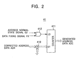
Fig. 2 is a diagram showing an internal configuration
of an address counter 41 of the information
recording/reproducing apparatus shown in Fig. 1;
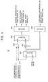
Fig. 3 is a diagram showing an internal configuration
of a timing-signal generation circuit 50 of the information
recording/reproducing apparatus shown in Fig. 1;
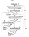
Fig. 4 is a diagram showing one example of a
synchronization control routine to be executed in the
synchronization control circuit 40;
Fig. 5 is a state transition diagram showing the state
of the address counter 41 and the state of the timing-signal
control circuit 50 when the synchronization control circuit
40 carries out a synchronization control process according
to a synchronization control routine shown in Fig. 4;
Fig. 6 is a diagram showing another example of a
synchronization control routine to be executed in the
synchronization control circuit 40;
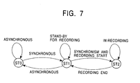
Fig. 7 is a state transition diagram showing the state
of the timing-signal generation circuit 50 when the
synchronization control circuit 40 carries out a
synchronization control process according to a
synchronization control routine shown in Fig. 6;
Fig. 8 is a diagram showing another example of a
synchronization control routine to be executed in the
synchronization control circuit 40;
Fig. 9 is a state transition diagram showing the state
of the address counter 41 and the state of the timing-signal
generation circuit 50 when the synchronization control
circuit 40 carries out a synchronization control process
according to a synchronization control routine shown in Fig.
7;
Fig. 10 is a diagram showing another example of a
synchronization control routine to be executed in the
synchronization control circuit 40;
Fig. 11 is a state transition diagram showing the
state of the address counter 41 and the state of the timing-signal
generation circuit 50 when the synchronization
control circuit 40 carries out a synchronization control
process according to a synchronization control routine shown
in Fig. 10;
Fig. 12 is a diagram showing another example of a
synchronization control routine to be executed in the
synchronization control circuit 40;
Fig. 13 is a state transition diagram showing the
state of the timing-signal generation circuit 50 when the
synchronization control circuit 40 carries out a
synchronization control process according to a
synchronization control routine shown in Fig. 12;
Fig. 14 is a diagram showing another example of a
synchronization control routine to be executed in the
synchronization control circuit 40; and
Fig. 15 is a state transition diagram showing the
state of the address counter 41 and the state of the timing-signal
generation circuit 50 when the synchronization
control circuit 40 carries out a synchronization control
process according to a synchronization control routine shown
in Fig. 14.
DETAILED DESCRIPTION OF THE INVENTION
Embodiments of the present invention will be described
in detail with reference to the drawings.
Fig. 1 is a diagram showing a configuration of an
information recording/reproducing apparatus for recording or
reproducing information data to or from a recording disk 30.
In Fig. 1, a recording/modulation circuit 31 supplies
the recording/reproducing head 32 with a modulated record
signal obtained by modulating the information data to be
recorded to the recording disk 30 according to a
predetermined record-modulation scheme. The recording disk
30 is previously recorded with a disk address indicating a
position on the disk and a synchronization signal serving to
take synchronization timing during control of
recording/reproducing. Incidentally, the disk address and
the synchronization signal are modulated based on the record
modulation scheme. The recording/reproducing head 32
irradiates a recording or reading beam of light onto a
surface of the recording disk 30 rotated by the spindle
motor 33. Namely, upon recording information data to the
recording disk 30, the recording/reproducing head 32
irradiates a recording light beam according to the modulated
record signal onto the surface of the recording disk 30.
Meanwhile, when reproducing information data from the
recording disk 30, the recording/reproducing head 32
irradiates a reading light beam onto the surface of the
recording disk 30. In this process, the
recording/reproducing head 32 performs a photoelectric
conversion on the reflection light of from the surface of
the recording disk 30, to generate a readout signal. This
signal is supplied to the respective ones of an information-data
reproducing circuit 34, an address demodulating circuit
35 and a synchronism detecting circuit 36. The information-data
reproducing circuit 34 carries out a predetermined
demodulating process on the readout signal, thereby
restoring the information data recorded on the recording
disk 30 and outputting it as reproduced information data.
The address demodulating circuit 35 carries out a
demodulating process on the readout signal according to an
address demodulated timing signal AX supplied from a timing-signal
generation circuit 50 (referred later). Due to the
demodulating process, the address demodulating circuit 35
demodulates an on-disk address and supplies the address data
AD representative of that on-disk address to an error
detecting circuit 37 and error correcting circuit 38.
The error detecting circuit 37 carries out an error
detecting process on the address data AD. Due to the error
detecting process, the error detecting circuit 37 generates,
for each 1-code block of address data AD, an error zero
signal E0 in logic level 0 when an error exists in the
address data AD and in logic level 1 when it does not exist
therein, to supply it to a synchronization control circuit
40. Furthermore, the error detecting circuit 37 generates,
for each 1-code block of address data AD, an uncorrectable
signal ER in logic level 0 when the address data AD can be
error-corrected and in logic level 1 when it cannot be
error-corrected, to supply it to a consecutive uncorrectable
states counter 39.
The consecutive uncorrectable states counter 39 counts
the number of times that the uncorrectable signal ER
consecutively assumes a logic level 1, and supplies a
consecutive uncorrectable states signal FN representative of
that number of times to the synchronization control circuit
40. Namely, the consecutive uncorrectable states counter 39
supplies the synchronization control circuit 40 with a
consecutive uncorrectable states signal FN representative of
the number of times that the address data AD is
consecutively uncorrectable in each code block. Incidentally,
the consecutive uncorrectable states counter 39 resets its
count value whenever the uncorrectable signal ER takes a
logic level 0.
The error correcting circuit 38 carries out an error
correction process on the address data AD. The address data
error-corrected by this error correction process is supplied
as corrected address data ADR to the respective ones of an
address counter 41, a recording/reproducing control circuit
42 and a continuous change number counter 43.
Fig. 2 is a diagram showing an internal configuration
of the address counter 41.
In Fig. 2, an adder 410 supplies a value the corrected
address data ADR is added by "1" to a load-data terminal DT
of a counter 411. An AND gate 412 supplies a data load
signal in logic level 1 to a data load control terminal LD
only when an address normal-state signal G2 in logic level 1
is supplied from the synchronization control circuit 40 and
a data fixing signal FX in logic level 1 is supplied from
the timing-signal generation circuit 50. The counter 411
makes a count-up operation to count up by one each time a
predetermined time period is elapsed, to output a current
count value as generated address data ADC. Incidentally, the
counter 411, when supplied by a data-load signal in logic
level 1, takes in as a count initial value a value the
corrected address data ADR is added by 1, to make a count-up
operation as in the above continuing from that count initial
value. Incidentally, the counter 411, when its count value
reaches a predetermined maximum value, resets the count
value to 0, thereby continuing the count-up operation as in
the above.
With this configuration, the address counter 41
supplies, as generated address data ADC, a current count
value obtained in the count up operation to the
recording/reproducing control circuit 42. In this process,
in the case that a data fixing signal FX in logic level 1
has been supplied during supplying an address normal-state
signal G2 in logic level 1, a value the address data ADR is
added by 1 is taken in as a count initial value, to make a
count-up operation continuing from that count initial value.
A consecutive changes counter 43 counts the number of
times the corrected address data ADR increases or decreases
by 1 at one time, to supply a continuous address change
number signal AN representative of that number of times to
the synchronization control circuit 40. Incidentally, the
consecutive changes counter 43 resets its count value to 0
when the corrected address data ADR increases (or decreases)
two or more after a lapse of a predetermined period of time,
i.e. when the corrected address data ADR is discontinued in
its one-by-one continuous increase (or decrease).
The recording/reproducing control circuit 42 controls
the recording/reproducing head 32, the spindle motor 33 and
the slider mechanism (not shown) for moving the
recording/reproducing head 32 radially of the disk, in order
to carry out various recording and reproducing operations on
the information recording/reproducing apparatus according to
various operations by the user. Incidentally, during
recording, the recording/reproducing control circuit 42
searches for a on-disk position on the basis of the
generated address data ADC or corrected address data ADR, in
order to initiate recording at a desired disk position on
the recording disk 30.
The synchronism detecting circuit 36 carries out a
demodulating process on the readout signal according to a
synchronization demodulation timing signal SX supplied from
the timing-signal generation circuit 50 (referred later),
thereby demodulating a synchronization signal. The
synchronization detection circuit 36 supplies a
synchronization detection signal SYC containing a
synchronization pulse to shift from logic level 0 to logic
level 1 in the detection timing of the synchronization
signal demodulated by the demodulating process, to the
synchronization control circuit 40, synchronism-abnormality
detecting circuit 44 and timing-signal generation circuit 50.
The synchronism-abnormality detecting circuit 44, when
the synchronization pulse on a synchronization detection
signal SYC has a predetermined period T, supplies the
synchronization control circuit 40 with an synchronism-abnormality
detection signal AB in the logic level 0
representative of "synchronism abnormality absent".
Meanwhile, when the synchronization pulse on a
synchronization detection signal SYC has a period not the
predetermined period T, the synchronism-abnormality
detecting circuit 44 supplies the synchronization control
circuit 40 with an synchronism-abnormality detection signal
AB in the logic level 1 representative of "synchronism
abnormality present". Namely, the synchronism abnormality
detecting circuit 44 supplies the synchronization control
circuit 40 with an synchronism-abnormality detection signal
AB in the logic level 0 when a synchronization signal can be
correctly read from the recording disk 30 and in the logic
level 1 when a synchronization signal cannot be correctly
read from the recording disk 30.
The timing-signal generation circuit 50 generates an
address demodulated timing signal AX, synchronization
demodulation timing signal SX and temporary synchronization
read timing signal SSX as noted before, on the basis of a
synchronization detection signal SYC and a synchronization
command signal G1 supplied from the synchronization control
circuit 40. The timing-signal generation circuit 50 supplies
an address demodulated timing signal AX and a
synchronization demodulation timing signal SX respectively
to the address demodulating circuit 35 and the synchronism
detecting circuit 36, and a synchronization demodulation
timing signal SX and a temporary synchronization read timing
signal SSX to the synchronization control circuit 40.
Furthermore, the timing-signal generation circuit 50
generates a data fixing signal FX as noted before depending
upon the synchronization detection signal SYC and
synchronization command signal G1, and supplies it to the
address counter 41.
Fig. 3 is a diagram showing an example on an internal
configuration of the timing-signal generation circuit 50.
In Fig. 3, a counter 501 takes in an initial value
whenever a synchronization detection signal SYC in logic
level 1 is supplied from the synchronism detecting circuit
36. This initial value is counted up each time a
predetermined period of time elapses, whereby a count value
is obtained and supplied to a decoder 500 and adder 502.
Incidentally, the counter 501, when its count value reaches
a predetermined maximum value, resets the count value to 0,
thus continuously carrying out the count-up operation. The
decoder 500 generates a pulse signal which is to shift from
logic level 0 to logic level 1 when the count value of the
counter 501 coincides with a predetermined count value, and
outputs it as a temporary synchronization read timing signal
SSX. An adder 502 supplies a value of the counter value of
the counter 501 added by "1" to a load-data terminal DT of a
counter 503. An AND gate 504 supplies a data load signal in
logic level 1 to the data load control terminal LD of the
counter 503 only when a synchronization command signal G1 in
logic level 1 is supplied from the synchronization control
circuit 40 and the synchronization detection signal SYC is
in logic level 1. The counter 503 makes a count-up operation
to count up by one each time a predetermined period of time
is elapsed, and supplies a current count value to the
decoder 505. Incidentally, the counter 503, when supplied by
a data-load signal in logic level 1, takes in as a count
initial value a value the count value of the counter 501 is
added by 1, to make a count-up operation continuing from the
count initial value. Meanwhile, the counter 503, when its
count value reaches a predetermined maximum value, resets
the count value to 0, to continue the count-up operation.
When the count value of the counter 503 coincides with a
predetermined first count value, a decoder 505 generates a
pulse signal that is to shift from logic level 0 to logic
level 1 and outputs it as an address demodulated timing
signal AX. Meanwhile, when the count value of the counter
503 coincides with a predetermined second count value, the
decoder 505 generates a pulse signal that is to shift from
logic level 0 to logic level 1 and outputs it as a
synchronization demodulation timing signal SX. Meanwhile,
when the count value of the counter 503 coincides with a
predetermined third count value, the decoder 505 generates a
data fixing signal FX in logic level 1 representing that the
process on 1-code block is completed in the error detecting
circuit 37 and error correcting circuit 38.
The synchronization control circuit 40 identifies a
state of the disk address and synchronization signal
reproduced from the recording disk 30 by a procedure
according to a synchronization control routine as shown in
Fig. 4. Depending upon an identification result, it controls
the address counter 41 and timing-signal generation circuit
50.
In Fig. 4, first, the synchronization control circuit
40 supplies a synchronization command signal G1 in logic
level 1 to the timing generation circuit 50 (step S40). By
executing the step S40, the counter 503 of the timing
generation circuit 50 takes in a predetermined counter
initial value each time a synchronization detection signal
SYC in logic level 1 is supplied, thus making a count-up
operation. Due to this, from the decoder 505 is outputted a
data fixing signal FX, address demodulated timing signal AX
and synchronization demodulation timing signal SX as noted
before in timing synchronization with the synchronization
detection signal SYC. After executing the step S40, the
synchronization control circuit 40 supplies the address
counter 41 with an address normal-state signal G2 in logic
level 0 representative of not having acquired a normal
address (step S41). By executing the step S41, the counter
41 of the timing generation circuit 50 operates by itself.
Next, the synchronization control circuit 40 determines
whether or not the synchronism-abnormality detection signal
AB is in level 1 representative of a synchronism abnormality
(step S42). While, in the step S42, the synchronism-abnormality
detection signal AB is in logic level 1, i.e. if
determined that a synchronization signal could not have been
read from the recording disk 30, the synchronization control
circuit 40 returns to the step S40 and repetitively executes
the foregoing operation.
Meanwhile, in the case, in the step S42, the
synchronism-abnormality detection signal AB is not in logic
level 1, i.e. in the case it is determined that a
synchronization signal could have been correctly read from
the recording disk 30, the synchronization control circuit
40 supplies a synchronization command signal G1 in logic
level 0 to the timing-signal generation circuit 50 (step
S43). By executing the step S43, the counter 503 of the
timing generation circuit 50 operates by itself. Next, the
synchronization control circuit 40 determines whether or not
an error zero signal E0 is in logic level 1 representative
of a state free of error (step S44). In the step S44, when
it is determined that the error zero signal E0 is not in
logic level 1, i.e. an error exist in the address data AD,
the synchronization control circuit 40 supplies the address
counter 41 with an address normal-state signal G2 in logic
level 0 representative of not having acquired a normal
address (step S45). By executing the step S45, the counter
41 of the timing generation circuit 50 operates by itself.
Next, the synchronization control circuit 40 determines
whether or not the address continuous changes signal AN
represents an address continuous changes greater than a
predetermined number P (step S46). If it is determined in
step S46 that the address continuous changes signal AN is
not greater than the predetermined number P, the
synchronization control circuit 40 returns to the step S42
and repetitively executes the foregoing operation.
Meanwhile, If it is determined in the step S44 that
the error zero signal E0 is in logic level 1, the
synchronization control circuit 40 supplies the address
counter 41 with an address normal-state signal G2 in logic
level 1 representative of having acquired a normal address
(step S47). By executing the step S47, the address counter
41 takes in as a counter initial value a value the corrected
address data ADR is added by 1 each time a data fixing
signal FX in logic level 1 is supplied from the timing-signal
generation circuit 50, and makes a count-up operation
continuing from that value. Namely, the address counter 41
creates generated address data ADC on the basis of the
normal corrected address data ADR reproduced from the
recording disk 30. On the other hand, if it is determined in
the step S46 that the address continuous changes signal AN
is greater than the predetermined number P, the error zero
signal E0 is in logic level 0 and the address continuous
changes signal AN is greater than the predetermined number P.
Hence, the address counter 41 makes a count-up operation.
Next, the synchronization control circuit 40 determines
whether or not the consecutive uncorrectable states signal
FN represents the number of times greater than a
predetermined number of times Q (step S48). In the step S48,
if the consecutive uncorrectable states signal FN is
determined not greater than the predetermined number of
times Q, the synchronization control circuit 40 returns to
executing the step S44 and determines whether or not a
normal address has been acquired. In this duration, if it is
determined in step S48 that the uncorrectable continuous
number of times signal FN is greater than a required number
of times Q, the synchronization control circuit 40 returns
to executing the step S42 and repetitively executes the
foregoing operation.
Fig. 5 is a diagram showing a transition in the
setting state to the address counter 41 and timing-signal
generation circuit 50 when the synchronization control
circuit 40 carries out a synchronization control process
according to a synchronization control routine shown in Fig.
4.
At first, while it is determined that a
synchronization signal cannot be correctly read from the
recording disk 30 (step S42), supplied are a synchronization
command signal G1 in logic level 1 and an address normal-state
signal G2 in logic level 0, hence maintaining an
asynchronous state ST0 as shown in Fig. 5. In the
asynchronous state ST0, the counter 503 within the timing-signal
generation circuit 50 makes a re-synchronism process.
Namely, even in case the reproducing state is unstable,
various signals, such as data fixing signal FX, address
demodulated timing signal AX and synchronization
demodulation timing signal SX, are generated according to
the synchronization detection signal at that time. Meanwhile,
the address counter operates by itself.
Meanwhile, if it is determined that the
synchronization signal could have been correctly read out
(step S42), the process returns to a synchronization state
ST1 as shown in Fig. 5. In the synchronization state ST1, a
synchronization command signal G1 in logic level 0 is
supplied to the timing-signal generation circuit 50 (step
S43). Due to this, the counter operates by itself and the
timing-signal generation circuit 50 begins to generate a
data fixing signal FX, address demodulated timing signal AX
and synchronization demodulation timing signal SX
synchronization in phase with the synchronization detection
signal SYC. In this duration, if the corrected address data
ADR reproduced from the recording disk 30 has been
determined not changed consecutively a number of times
greater than a predetermined number P (step S46) and a
synchronization signal could not have been correctly read
out (step S42), then the process returns to an asynchronous
state ST0. Due to this, a synchronization command signal G1
in logic level 1 is sent to execute a re-synchronism process.
On the other hand, when determined that there is no error
in the corrected address data ADR (step S44), i.e. when the
corrected address data ADR is determined as a correct
address, the process returns to an address normal state ST2.
In the address normal state ST2, an address normal
state signal G2 in logic level 1 is supplied to the address
counter 41 (step S47). Due to this, the address counter 41
takes in the corrected address data ADR and increases (or
decreases) the address data value thereof by 1 at one time,
thereby creating generated address data ADC and supplying it
to the recording/reproducing control circuit 42. If the
corrected address data ADR is determined having an error (E0
= "1") and the corrected address data ADR is determined
having continuously changed a number of times greater than
the predetermined number P, an address normal state signal
G2 in logic level 0 is supplied to increase (or decrease) by
1 at one time the value of address data acquired before. In
this duration, the address normal state ST2 is maintained
unless the address data AD read out from the recording disk
30 and demodulated is determined to be uncorrectable
consecutively a number of times greater than a predetermined
number of times Q (step S48). Meanwhile, in the case that
the address data AD is determined to be uncorrectable
consecutively a number of times greater than the
predetermined number of times Q, i.e. in the case the
corrected address data ADR is determined an incorrect
address, the process returns to a synchronization state ST1.
Namely, in the case that the corrected address data ADR is
determined as not a correct address, it is determined that
there is a possibility of going out of synchronism under
influence of a certain external disturbance, and the process
returns to the synchronization state ST1 where determination
is made for a synchronization state. As a result, in the
case of a determination of going out of synchronism, a
synchronization command signal in logic level 1 is sent to
thereby effect a re-synchronism process (loading the counter
503 with an initial value in timing synchronization with the
synchronization detection signal SYC).
In other words, once the corrected address data ADR is
determined a correct address, even if the synchronization
signal read from the recording disk 30 be temporarily
disturbed, a re-synchronism process is put into stand-by for
execution until the corrected address data ADR is determined
an incorrect address.
Accordingly, in the synchronization control process by
the synchronization control circuit 40, a re-synchronism
process cannot be effected by a temporary disturbance or so
of a synchronization signal due to an external disturbance,
such as crosstalk from an adjacent track or surface damage
of the recording disk. Information data recording can be
swiftly completed without discontinuing the recording
operation.
Meanwhile, in the above embodiment, synchronization
state was shifted from ST1 to ST2 (or from ST1 to ST2) in
accordance with an error state of address data AD.
Alternatively, transition of synchronization state may be
carried out from ST1 to ST2 (or from ST1 to ST2) by starting
or ending a record to the recording disk 30.
Fig. 6 is a diagram showing another example of
synchronization control routine made in view of that point.
In Fig. 6, the synchronization control circuit 40
first supplies a synchronization command signal G1 in logic
level 1 to the timing-signal generation circuit 50 (step
S60). By executing the step S60, the counter 503 of the
timing-signal generation circuit 50 takes in a predetermined
counter initial value each time a synchronization detection
signal SYC in logic level 1 is supplied, thus effecting a
count-up operation. Due to this, from the decoder 505 is
outputted a data fixing signal FX, address demodulated
timing signal AX and synchronization demodulation timing
signal SX as noted before in timing synchronization with the
synchronization detection signal SYC. After executing the
step S60, the synchronization control circuit 40 determines
whether or not the synchronism-abnormality detection signal
AB is in level 1 representative of an abnormality of
synchronism (step S61). While, in the step S61, the
synchronism-abnormality detection signal AB is in logic
level 1, i.e. while determined that a synchronization signal
could not have been correctly read from the recording disk
30, the synchronization control circuit 40 returns to the
step S60 and repetitively executes the foregoing operation.
Meanwhile, if, in the step S61, the synchronism-abnormality
detection signal AB is not in logic level 1, i.e.
if determined that a synchronization signal could have been
correctly read from the recording disk 30, the
synchronization control circuit 40 supplies a
synchronization command signal G1 in logic level 0 to the
timing-signal generation circuit 50 (step S62). By executing
the step S62, the counter 503 of the timing-signal
generation circuit 50 operates by itself. After executing
the step S62, the synchronization control circuit 40 then
determines whether or not to the recording disk 30 has been
supplied, from a recording/reproducing control circuit 42, a
record start signal notifying that recording information
data is to be started (step S63). If it is determined in
step S63 that a record starting signal has not been supplied,
the synchronization control circuit 40 returns to executing
the step S61 and repetitively executes the foregoing
operation. Meanwhile, if it is determined in step S63 that a
record starting signal has been supplied, the
synchronization control circuit 40 then repetitively
determines whether or not a record ending signal notifying
to end the recording of information data to the recording
disk 30 has been supplied from the recording/reproducing
control circuit 42 until a record ending signal is supplied
(step S64). If it is determined in the step S64 that a
record ending signal has been supplied, the synchronization
control circuit 40 returns to executing the step S61 and
repetitively executes the foregoing operation.
Fig. 7 is a diagram showing a transition in a setting
state to the timing-signal generation circuit 50 when the
synchronization control circuit 40 makes a synchronization
control process according to a procedure shown in Fig. 6.
At first, while a synchronism-abnormality detection
signal AB is in logic level 1, i.e. it is determined that a
synchronization signal cannot be correctly read from the
recording disk 30 (step S61), maintained is an asynchronous
state ST0 as shown in Fig. 5. In the asynchronous state ST0,
the counter 503 within the timing-signal generation circuit
50 carries out a re-synchronism process according to a
synchronization command signal G1 in logic level 1, thereby
generating a data fixing signal FX, an address demodulated
timing signal AX and a synchronization demodulation timing
signal SX.
Meanwhile, if it is determined that a synchronization
signal could have been correctly read from the recording
disk 30, the process returns to a synchronization state ST1
as shown in Fig. 7. In the synchronization state ST1, a
synchronization command signal G1 in logic level 0 is
supplied to the timing-signal generation circuit 50 (step
S62). Due to this, the timing-signal generation circuit 50
begins to generate a data fixing signal FX, address
demodulated timing signal AX and synchronization
demodulation timing signal SX that is synchronization in
phase with the synchronization detection signal SYC. In this
duration, if it is determined that a record starting signal
has been supplied (step S63), the process shifts to a
recording state ST2 shown in Fig. 7. Meanwhile, if a record
starting signal is determined to be not supplied and a
synchronization signal is determined not to be correctly
read out (step S61), the process shifts to an asynchronous
state ST0.
In the recording state ST2, the recording state ST2 is
maintained until a record ending signal is supplied (step
S64). In this process, if it is determined supplied by a
record ending signal, the process shifts to a
synchronization state ST1. Namely, the recording state ST2
is maintained during recording to the recording disk 30. In
this duration, after recording is over, the process returns
to a synchronization state ST1 and carries out a
synchronizing process, monitoring the synchronization state.
Herein, if a synchronism-abnormality signal is detected, a
re-synchronism process (loading an initial value to the
counter 503 in timing synchronization with the
synchronization detection signal SYC) is carried out. In
other words, during a record operation, even if a temporary
disturbance be caused in the synchronization signal read
from the recording disk 30, the record operation is
continued without executing a re-synchronism process.
Accordingly, in the synchronization control process as
shown in Figs. 6 and 7, re-synchronism process cannot be
effected even if the synchronization signal is disturbed by
external disturbance, such as crosstalk from an adjacent
track or surface damage of the recording disk. Accordingly,
information data recording can be swiftly completed without
discontinuing the recording operation.
Incidentally, the synchronization control circuit 40
may implement a synchronization control process combined
with the synchronization control process shown in Figs. 4
and 5 and the synchronization control process shown in Figs.
6 and 7.
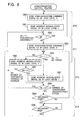
Fig. 8 is a diagram showing a synchronization control
routine made in view of that point.
Incidentally, the steps S80 - S88 in the
synchronization control routine shown in Fig. 8 are similar
to the steps S40 - S48 shown in Fig. 4. It is noted that, in
the synchronization control routine shown in Fig. 8, in the
case that the continuous uncorrectable number of times in
the address data AD is determined smaller than a
predetermined number of times or correctable in step S88,
then the synchronization control circuit 40 determines
whether or not a record starting signal has been supplied
(step S89). When it is determined in the step S89 that a
record starting signal has not been supplied, the
synchronization control circuit 40 returns to step S84 and
determines whether a normal address is acquired or not.
Meanwhile, when it is determined in the step S89 that a
record starting signal has been supplied, then the
synchronization control circuit 40 repetitively determines
whether or not a record ending signal is supplied or not
until such a record ending signal is supplied (step S90).
In the step S90, when a record ending signal is determined
supplied, the synchronization control circuit 40 returns to
executing the step S84.
Fig. 9 is a diagram showing a transition of a setting
state to the address counter 41 and timing-signal generation
circuit 50 when the synchronization control circuit 40
carries out a synchronization control process according to a
procedure shown in Fig. 8.
Incidentally, in Fig. 9, the transition in the
asynchronous state ST0, synchronization state ST1 or address
normal state ST2 is similar to that shown in Fig. 5. In Fig.
9, when a record start signal is determined supplied in the
address normal state ST2 (step S89), the process shifts to a
recording state ST3. In the recording state ST3, the
recording state ST3 is maintained until a record ending
signal is determined supplied (step S90). Herein, if a
record ending signal is determined supplied, the process
shifts to an address normal state ST2. Namely, during a
recording to the recording disk 30, the recording state ST3
is maintained even if the corrected address data read from
the recording disk 30 is not correct so that the process
shifts to an address normal state ST2 after the recording
operation is over.
Accordingly, because a re-synchronism process is
placed stand-by during the period of time the corrected
address data ADR is being determined a correct address or
during a recording operation, information data recording can
be swiftly completed without discontinuing recording.
Fig. 10 is a diagram showing another example of
synchronization control routine to be carried out by the
synchronization control circuit 40.
In Fig. 10, at first, the synchronization control
circuit 40 supplies a synchronism command signal G1 in logic
level 0 to the timing signal control circuit 50 (step S100).
By executing the step S100, the counter 503 of the timing-signal
generation circuit 50 operates by itself. After
executing the step S100, the synchronization control circuit
40 supplies the address counter 41 with an address normal-state
signal G2 in logic level 0 representative of not
having acquired a normal address (step S101). By executing
the step S101, the counter 41 of the timing-signal
generation circuit 50 operates by itself. Next, the
synchronization control circuit 40 determines whether or not
the temporary synchronization read timing signal SSX,
generated based on a count value of the counter 501 of the
timing-signal generation circuit 50, is in the same timing
as the synchronization detection signal SYC (step S102). If
it is determined in step S102 that the both are not in the
same timing, the synchronization control circuit 40 returns
to the step S100 and repetitively carries out the foregoing
operation. Meanwhile, if it is determined in the step S102
that the both are in the same timing, the synchronization
control circuit 40 supplies a synchronism command signal G1
in logic level 0 to the timing signal control circuit 50
(step S103). By executing the step S103, the counter 503 of
the timing-signal generation circuit 50 takes in a
predetermined counter initial value each time a
synchronization detection signal SYC in logic level 1 is
supplied, thus making a count-up operation. Due to this,
from the decoder 505 is outputted a data fixing signal FX,
address demodulated timing signal AX and synchronization
demodulation timing signal SX in timing synchronization with
the synchronization detection signal SYC. Next, the
synchronization control circuit 40 determines whether or not
the synchronism demodulated timing signal SX, generated
based on a count value of the counter 503 of the timing-signal
generation circuit 50, is in the same timing as the
synchronization detection signal SYC (step S104). If it is
determined in step S104 that the both are not in the same
timing, the synchronization control circuit 40 returns to
the step S102 and repetitively carries out the foregoing
operation. Meanwhile, if it is determined in the step S104
that the synchronism modulation timing signal SX and the
synchronization detection signal SYC are in the same timing,
the synchronization control circuit 40 supplies a
synchronism command signal G1 in logic level 1 to the timing
signal control circuit 50 (step S105). By executing the step
S105, the counter 503 of the timing-signal generation
circuit 50 operates by itself. Next, the synchronization
control circuit 40 determines whether or not an error zero
signal E0 is in logic level 1 representative of an error-free
state (step S106). In the step S106, if it is
determined that the error zero signal E0 is not in logic
level 2, i.e. if an error exist in the address data AD, the
synchronization control circuit 40 supplies the address
counter 41 with an address normal-state signal G2 in logic
level 0 representative of not having acquired a normal
address (step S107). By executing the step S107, the counter
41 of the timing-signal generation circuit 50 operates by
itself. Then, the synchronization control circuit 40
determines whether or not a continuous change address number
signal AN represents a number of continuous changes of
address greater than a predetermined number P (step S108).
If it is determined in the step S108 that the number
represented by continuous change address number signal AN is
not greater than the predetermined number P, the
synchronization control circuit 40 returns to the step S104
and repetitively carries out the foregoing operation.
Meanwhile, if the error zero signal E0 is determined
in logic level 1 in the step S106, the synchronization
control circuit 40 supplies the address counter 41 with an
address normal-state signal G2 in logic level 1
representative of having acquired a normal address (step
S109). By executing the step S109, the address counter 41
takes in as a counter initial value a value the corrected
address data ADR is added by 1 each time a data fixing
signal FX in logic level 1 is supplied from the timing-signal
generation circuit 50, thus making a count-up
operation continuing from that value. Namely, the address
counter 41 creates generated address data ADC on the basis
of the normal corrected address data ADR reproduced from the
recording disk 30. Meanwhile, if the address continuous
changes signal AN is determined greater than a predetermined
umber P in the step S108, then the error zero signal E0 is
in logic level 0 and the address continuous changes signal
AN is greater than the predetermined number P. Accordingly,
the address counter 41 makes a count-up operation. Then, the
synchronization control circuit 40 determines whether or not
the consecutive uncorrectable states signal FN represents a
number greater than the predetermined number of times Q
(step S110). In the step S110, if the consecutive
uncorrectable states signal FN is determined not greater
than the predetermined number of times Q, the
synchronization control circuit 40 returns to executing the
step S106 and determines whether or not a normal address
have been acquired. In this duration, if the consecutive
uncorrectable states signal FN is determined greater than
the predetermined number of times Q in the step S110, the
synchronization control circuit 40 returns to executing the
step S104 and repetitively executes the foregoing operation.
Fig. 11 is a diagram showing a transition in the
setting state to the address counter 41 and timing-signal
generation circuit 50 when the synchronization control
circuit 40 carries out a synchronization control process
according to a synchronization control routine shown in Fig.
10.
At first, while the synchronization detection signal
SYC detected from the recording disk 30 and the temporary
synchronization read timing signal SSX generated based on a
count value of the counter 501 of the timing-signal
generation circuit 50 are determined not in the same timing
(step S102), the asynchronous state ST0 is maintained to
send a synchronism command signal G1 in logic level 0 and an
address normal-state signal G2 in logic level 0. In the
asynchronous state ST0, the counter 503 within the timing-signal
generation circuit 50 operates by itself. In timing
asynchronous with the synchronization signal, generated is a
data fixing signal FX, address demodulated timing signal AX
and synchronism demodulated timing signal SX.
Meanwhile, if the synchronization detection signal SYC
and the temporary synchronization read timing signal SSX are
determined in the same timing, the process shifts to a
temporary synchronization state ST1. In the temporary
synchronization state ST1, a synchronism command signal G1
in logic level 1 is sent to load the counter 503 with a
current count value of the temporary synchronism counter 501.
Then, determination is made as to whether or not the
synchronization detection signal SYC detected from the
recording disk 30 and the synchronism demodulated timing
signal SX generated based on a count value of the counter
503 of the timing-signal generation circuit 50 are in the
same timing (step S104). In this process, if it is
determined that the both are in the same timing, the process
shifts to a synchronization state ST2.
In the synchronization state ST2, a synchronism
command signal G1 in logic level 0 is sent and the counter
503 operates by itself. Due to this, the timing-signal
generation circuit 50 begins to generate a data fixing
signal FX, address demodulated timing signal AX and
synchronism demodulated timing signal SX synchronization in
phase with the synchronization detection signal SYC. In this
duration, in the case of a determination that the corrected
address data ADR reproduced from the recording disk 30 has
not changed consecutively a number of times greater than a
predetermined number P (step S108), the process is
maintained in the synchronization state ST2. Incidentally,
in this duration, in the case of a determination that the
synchronization detection signal SYC and the synchronism
demodulated timing signal SX are not in the same timing, the
process shifts up to a temporary synchronization state ST1.
Meanwhile, when not in temporary synchronism either, the
process shifts to an asynchronous state ST0. Meanwhile, in
the case of a determination that no error exists in the
corrected address data, i.e. in the case the corrected
address data ADR is determined a correct address, the
process shifts to an address normal state ST3. In the
address normal state ST3, a normal state signal G2 in logic
level 1 is supplied to the address counter 41 (step S109).
Due to this, the address counter 41 takes in the corrected
address data ADR and increases (or decreases) the address
data value thereof by 1 at one time, thereby creating
generated address data ADC and supplying it to the
recording/reproducing control circuit 42. In the case that
there is determined an error in the corrected address data
ADR (E0 = "1") and the corrected address data ADR is
determined changed continuously a number of times greater
than a predetermined number P, a normal-state signal G2 in
logic level 0 has been supplied to increase (or decrease)
the value of the before-obtained address data by 1 at one
time. In this duration, the address normal state ST3 is
maintained until the address data AD read from the recording
disk 30 is determined not correctable continuously a number
of times greater than a predetermined number of times Q
(step S110), i.e. until the corrected address data ADR is
determined an incorrect address. On the other hand, in the
case that the address data AD read from the recording disk
30 is determined not correctable continuously a number of
times greater than the predetermined number of times Q, the
process shifts to a synchronism state ST2. Namely, in the
case that the address data read from the recording disk 30
and correction-processed is determined an incorrect address,
the process shifts to an address normal state ST3,
synchronization state ST2, temporary synchronization state
ST1 and asynchronous state ST0 and then enters a re-synchronism
process routine (loading an initial value onto
the counter 503 in timing synchronization with the
synchronization detection signal SYC), making a
determination of going out of synchronism under influence of
a certain external disturbance. In other words, once the
process shifts to an address normal state ST3, re-synchronism
process is placed stand-by for execution until
it is determined that the corrected address data ADR is an
incorrect address and synchronism is placed out.
Accordingly, in also the synchronization control
process as shown in Figs. 10 and 11, even if a temporary
external disturbance occurs, information data recording can
be swiftly completed without discontinuing the recording
operation.
Meanwhile, Fig. 12 is a diagram showing another
example of synchronization control routine to be executed by
the synchronization control circuit 40.
In Fig. 12, at first, the synchronization control
circuit 40 supplies a synchronization command signal G1 in
logic level 0 to the timing-signal generation circuit 50
(step S120). By executing the step S120, the counter 503 of
the timing-signal generation circuit 50 operates by itself.
After executing the step S120, the synchronization control
circuit 40 determines whether or not the temporary
synchronization read timing signal SSX generated based on a
count value of the counter 501 of the timing-signal
generation circuit 50 is in the same timing as the
synchronization detection signal SYC (step S121). In the
case of a determination in the step S121 that the both are
not in the same timing, the synchronization control circuit
40 returns to the step S120 and repetitively carries out the
foregoing operation. Meanwhile, if it is determined in the
step S121 that the both are in the same timing, the
synchronization control circuit 40 supplies a synchronism
command signal G1 in logic level 1 to the timing-signal
generation circuit 50 (step S122). By executing the step
S122, the counter 503 of the timing-signal generation
circuit 50 takes in a predetermined counter initial value
each time a synchronization detection signal SYC in logic
level 1 is supplied, thus making a count-up operation. Due
to this, from the decoder 505 is outputted a data fixing
signal FX, address demodulated timing signal AX and
synchronization demodulation timing signal SX, as noted
before, in timing synchronization with the synchronization
detection signal SYC. After executing the step S122, the
synchronization control circuit 40 determines whether or not
the synchronism demodulated timing signal SX generated based
on a count value of the counter 503 of the timing-signal
generation circuit 50 and the synchronization detection
signal SYC are in the same timing (step S123). If it is
determined in the step S123 that the both are not in the
same timing, the synchronization control circuit 40 returns
to the step S121 and repetitively carries out the foregoing
operation. Meanwhile, if it is determined in the step S123
that the synchronism demodulated timing signal SX and the
synchronization detection signal SYC are in the same timing,
the synchronization control circuit 40 supplies a
synchronization command signal G1 in logic level 0 to the
timing-signal generation circuit 50 (step S124). By
executing the step S124, the counter 503 of the timing-signal
generation circuit 50 operates by itself. After
executing the step S124, the synchronization control circuit
42 determines whether or not from the recording/reproducing
control circuit 40 determines whether or not have been
supplied a record starting signal notifying to start a
recording of information data to the recording disk 30 (step
S125). In the case of a determination in the step S125 that
a record starting signal has not been supplied, the
synchronization control circuit 40 returns to executing the
step S123 and repetitively carries out the foregoing
operation. Meanwhile, in the case of a determination in the
step S125 that a record starting signal has been supplied,
the synchronization control circuit 40 then repetitively
determines whether or not from the recording/reproducing
control circuit 42 has been supplied a record ending signal
notifying to end the recording of information data to the
recording disk 30, until a record ending signal is supplied
(step S126). In the case of a determination in the step S126
that a record ending signal has been supplied, the
synchronization control circuit 40 returns to executing the
step S123 and repetitively carries out the foregoing
operation.
Fig. 13 is a diagram showing a transition in the
setting state to the timing-signal generation circuit 50
when the synchronization control circuit 40 carries out a
synchronization control process according to a
synchronization control routine shown in Fig. 12.
At first, while the synchronization detection signal
SYC detected from the recording disk 30 and the temporary
synchronization read timing signal SSX generated based on a
count value of the counter 501 of the timing-signal
generation circuit 50 are determined not in the same timing
(step S121), the asynchronous state ST0 is maintained to
send a synchronism command signal G1 in logic level 0. In
the asynchronous state ST0, the counter 503 within the
timing-signal generation circuit 50 operates by itself. In
timing asynchronous with the synchronization signal,
generated is a data fixing signal FX, address demodulated
timing signal AX and synchronism demodulated timing signal
SX.
Meanwhile, if it is determined that the
synchronization detection signal SYC and the temporary
synchronization read timing signal SSX are in the same
timing, the process shifts to a temporary synchronization
state ST1. In the temporary synchronization state ST1, a
synchronism command signal G1 in logic level 1 is sent to
load the counter 503 with a current count value of the
temporary synchronism counter 501. Then, determination is
made as to whether or not the synchronization detection
signal SYC detected from the recording disk 30 and the
synchronism demodulated timing signal SX generated based on
a count value of the counter 503 of the timing-signal
generation circuit 50 are in the same timing (step S123). In
this process, if it is determined that the both are in the
same timing, the process shifts to a synchronization state
ST2.
In the synchronization state ST2, a synchronism
command signal G1 in logic level 0 is sent and the counter
503 operates by itself. Due to this, the timing-signal
generation circuit 50 begins to generate a data fixing
signal FX, address demodulated timing signal AX and
synchronism demodulated timing signal SX synchronization in
phase with the synchronization detection signal SYC. In this
duration, in the case of a determination that a record
staring signal has been supplied (step S125), the process
shifts to a recording state ST3. In the recording state ST3,
this recording state ST3 is maintained until a record ending
signal is determined supplied (step S126). In this process,
if it is determined tha a record ending signal has been
supplied, the process shifts to a synchronization state ST2
and carries out a synchronizing process. In the case of a
determination of going out of synchronism, the process
shifts to a temporary synchronization state ST1. Furthermore,
in the case of a determination of also going out of
temporary synchronism, the process shifts to an asynchronous
state ST0 and carries out a re-synchronizing process.
Accordingly, during recording to the recording disk 30, even
if disturbance temporarily occurs due to external
disturbance such as crosstalk from the adjacent track,
damage on the recording disk surface or the like, the
process is placed in a stand-by state for re-synchronism
process.
Incidentally, the synchronization control circuit 40
may implement a synchronization control process combined
with the synchronization control process shown in Figs. 10
and 11 and the synchronization control process shown in Figs.
12 and 13.
Fig. 14 is a diagram showing a synchronization control
routine made in view of that point.
Incidentally, the steps S140 - S150 in the
synchronization control routine shown in Fig. 14 are similar
to the steps S100 - S110 shown in Fig. 10. It is noted that,
the synchronization control routine shown in Fig. 14, in the
case that the continuous uncorrectable number of times in
the address data AD is determined smaller than a
predetermined number of times or correctable in step S150,
then the synchronization control circuit 40 determines
whether or not a record starting signal has been supplied
(step S151). When it is determined in the step S151 that a
record starting signal has not been supplied, the
synchronization control circuit 40 returns to the step S146
and again determines whether or not a normal address has
been acquired. Meanwhile, when it is determined in the step
S151 that a record starting signal has been supplied, then
the synchronization control circuit 40 repetitively
determines whether or not a record ending signal is supplied
until such a record ending signal has been supplied (step
S152). In the step S152, when a record ending signal is
determined supplied, the synchronization control circuit 40
returns to the step S146 and again determines whether or not
a normal address has been acquired.
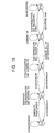
Fig. 15 is a diagram showing a transition of a setting
state to the address counter 41 and timing-signal generation
circuit 50 when the synchronization control circuit 40
carries out a synchronization control process according to a
procedure shown in Fig. 14.
At first, while the synchronization detection signal
SYC detected from the recording disk 30 and the temporary
synchronization read timing signal SSX generated based on a
count value of the counter 501 of the timing-signal
generation circuit 50 are determined not in the same timing
(step S142), the asynchronous state ST0 is maintained to
send a synchronism command signal G1 in logic level 0. In
the asynchronous state ST0, the counter 503 within the
timing-signal generation circuit 50 operates by itself. In
timing asynchronous with the synchronization signal,
generated is a data fixing signal FX, address demodulated
timing signal AX and synchronism demodulated timing signal
SX.
Meanwhile, if the synchronization detection signal SYC
and the temporary synchronization read timing signal SSX are
determined in the same timing, the process shifts to a
temporary synchronization state ST1. In the temporary
synchronization state ST1, a synchronism command signal G1
in logic level 1 is sent to load the counter 503 with a
current count value of the temporary synchronism counter 501.
Then, determination is made as to whether or not the
synchronization detection signal SYC detected from the
recording disk 30 and the synchronism demodulated timing
signal SX generated based on a count value of the counter
503 of the timing-signal generation circuit 50 are in the
same timing (step S144). In this process, if the both are
determined as in the same timing, the process shifts to a
synchronization state ST2.
In the synchronization state ST2, a synchronism
command signal G1 in logic level 0 is sent and the counter
503 operates by itself. Due to this, the timing-signal
generation circuit 50 begins to generate a data fixing
signal FX, address demodulated timing signal AX and
synchronism demodulated timing signal SX synchronization in
phase with the synchronization detection signal SYC. In this
duration, in the case of a determination that the corrected
address data ADR reproduced from the recording disk 30 has
not changed consecutively a number of times greater than a
predetermined number P (step S148) and a determination that
the synchronization detection signal SYC and the synchronism
demodulated timing signal SX are in the same timing (step
S144), the process is maintained in the synchronization
state ST2. Incidentally, in the case of a determination that
the synchronization detection signal SYC and the synchronism
demodulated timing signal SX are not in the same timing, the
process shifts up to a temporary synchronization state ST1.
Meanwhile, when not in temporary synchronism either, the
process shifts to an asynchronous state ST0. On the oher
hand, in the case of a determination that there is no error
in the corrected address data ADR (step S146), the process
shifts to an address normal state ST3. In the address normal
state ST3, an address normal-state signal G2 in logic level
1 is supplied to the address counter 41 (step S149). Due to
this, the address counter 41 takes in the corrected address
data ADR and increases (or decreases) the address data value
thereof by 1 at one time, thereby creating generated address
data ADC and supplying it to the recording/reproducing
control circuit 42. In the case that the corrected address
data ADR is determined having an error (E0 = "1") and the
corrected address data ADR is determined having continuously
changed a number of times greater than a predetermined
number P, an address normal-state signal G2 in logic level 0
is supplied to increase (or decrease) the value of address
data acquired before by 1 at one time. Incidentally, the
address normal state ST3 is maintained until the address
data AD is determined uncorrectable consecutively a number
of times greater than a predetermined number of times Q
(step S150), i.e. until the corrected address data ADR read
from the recording disk 30 and then error-corrected is
determined as an incorrect address. Herein, in the case that
the address data AD read from the recording disk 30 is
determined uncorrectable consecutively a number of times
greater than the predetermined number of times Q, the
process shifts to a synchronization state ST2. Namely, in
the case that the corrected address data is determined as an
incorrect address, determination is as going out of
synchronism under influence of a certain external
disturbance, and the process returns to the synchronization
state ST2 and carries out a re-synchronism process. In other
words, once the the process shifts to an address normal
state ST3, even if the synchronization signal read from the
recording disk 30 be temporarily disturbed, re-synchronism
process is not carried out until the corrected address data
ADR is determined an incorrect address.
Meanwhile, in the case of a determination that the
address data AD is not uncorrectable consecutively a number
of times greater than the predetermined number of times Q
and a determination that a record starting signal notifying
to start a recording to the recording disk 30 has been
supplied (step S151), the process shifts to a recording
state ST4. In the recording state ST4, this determining
operation is repetitively executed until it is determined
that a record ending signal has been supplied (step S152).
In this process, if a record ending signal is determined
supplied, the process shifts to an address normal state ST3.
Namely, during recording to the recording disk 30, the
recording state ST4 is maintained. In this duration, after
ending the recording, the process shifts to an address
normal state ST3.
Therefore, according to the synchronization control
process shown in Figs. 13 and 14, even if there is a
temporary disturbance in a synchronization signal read from
the recording disk 30, re-synchronism process is not carried
out in the case the corrected address data after error
correction is of a proper address or during recording.
As described above, in the synchronization control
circuit 40, in the case that the corrected address data read
from the recording disk 30 and then error-corrected is
determined as a proper address, a re-synchronism process is
placed stand-by for execution until the corrected address
data is determined as an incorrect address. Meanwhile, the
synchronization control circuit 40 similarly puts a re-synchronism
process into stand-by for execution during
recording to the recording disk 30.
Therefore, according to the operation, even if a
temporary external disturbance be caused by the crosstalk
from the adjacent tracks or the dusts, dirt, mars or the
like on the recording disk surface, information data
recording can be swiftly completed without discontinuing
recording operation.
Incidentally, in the above embodiment, a synchronism
process is implemented when determining the corrected
address data as an incorrect address or upon ending a
recording operation. However, re-synchronism process may be
forcibly effected depending upon so-called a search
operation that is to forcibly transfer the
recording/reproducing head 32 to a predetermined recording
position.