Technical Field
The present invention relates to a plasma display panel
display device and its driving method.
Background Art
A plasma display panel (PDP) display device includes a
PDP unit being composed of a thin front glass panel and a thin
back glass panel arranged facing each other via a plurality
of barrier ribs, having fluorescent layers of each of the colors
red (R), green (G), and blue (B) applied between the barrier
ribs, and discharge gas enclosed in a discharge space which
is a gap between the two glass panels. A plurality of pairs
of display electrodes, each pair consisting of a scan electrode
and a sustain electrode, are formed on the front glass panel.
Also, a plurality of address electrodes are aligned on the back
glass panel, so as to be perpendicular to the display electrodes,
the discharge space being between the address electrodes and
display electrodes. In a subfield (which is described later) ,
each of the electrodes is applied with pulses such as
initialization pulses, scan pulses, write pulses, sustain
pulses, and erase pulses, based on, for example, the drive
waveform process shown in Fig. 15, so that fluorescent light
is emitted according to the electric discharge generated in
the discharge gas. A PDP display device having this kind of
construction is superior to a conventional CRT display in that
it does not involve problems including limitations in viewing
angles and increased depth and weight when a large screen PDP
is produced, as a large screen conventional display CRT does.
There is much demand for this kind of large screen, high
definition PDP display device, and at present PDP display
devices of 50 inches or more in size are being commercially
produced.
Note that when a television video is shown on a display
using an analog color television video signal system, one
second of an image is constructed from 60 frames (or fields).
In a basic PDP display device, because image display is
basically possible only by illumination and extinction, a
method for displaying halftones is used in which the
illumination time corresponding to each of the colors red (R) ,
green (G) and blue (B) is time-shared, as shown in the frame
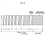
structure diagram Fig. 16. For example a plurality of level
gradation display times are in accordance with a combination
of eight subfields which constitute 1 (TV) frame. The relative
luminance ratios of each of the eight subfields are assigned,
in ascending order, binary weights such as 1, 2, 4, 8, 16, 32,
64, 128, and display, for example, a total of 256 gradations
(level 0 gradation to level 255 gradation) according to a
combination of the different weights of the 8 bit relative
luminance ratio. Further, in order to maintain a sufficient
brightness during actual operation, a number of sustain pulses
to be applied during the discharge sustain period of each
subfield is substantially set in proportion with the assigned
weight. It is supposed that the number of pulses, in the
described relative luminance ratio order is 3, 7, 15, 31, 63,
127, 255, 511 (wherein "level 0 gradation", "level 1 gradation",
"level 2 gradation" to "level 8 gradation" and so on, which
are described later, show specific level gradations included
in 256 total gradations).
A PDP display device having the above characteristics
incurs the following problems during low-level gradation
display.
Namely, in display it is generally desirable that the
relative luminance ratio decreases as the gradation level of
the display becomes lower, as this allows dark gradation
display to be expressed smoothly. When using a CRT to display,
of the total 256 gradations, level 0 gradation, and level 1
gradation which has a relative luminance ratio corresponding
to the smallest weight, the luminance ratio showing the
difference in gradation level is close to 0cd/m2, and a smooth
gradation display time is possible. However in a PDP display
device, the luminance ratio of level 0 gradation and level 1
gradation is no less than 2cd/ m2, therefore it is difficult
to display such a change in luminance as smoothly as in a CRT
device.
In response to this problem, if the sustain pulse rate
is set at a very low gradation setting, light emission gained
by sustain pulses during the level 1 gradation display time
can be restricted, however because light emission is left over
from the initialization pulse, write pulse, and erase pulse,
luminance cannot be substantially lowered. Further, even if
gradation display time is falsely attempted using error
diffusion processing (dither method), error diffusion noise
is noticeable on the screen because the gradation level is low,
and rather than an effective error diffusion result being
gained, a new problem of deterioration in picture quality
arises.
Disclosure of the Invention
In consideration of the abovementioned problems, the aim
of the present invention is to provide a PDP display device
and driving method therefor, capable of offering superior
performance during low-level gradation display when
performing multi-level gradation display.
In order to solve the abovementioned problems, the
present invention is a PDP display apparatus driving method
for performing multi-level gradation display by constituting
one frame of a plurality of subfields assigned different
weights, wherein in a subfield in which a relative luminance
ratio corresponds to a lowest weight, display is performed
according to discharges in two periods only, the periods being
an initialization period and a write period.
According to this driving method, because emission
luminance of the subfield having the lowest relative luminance
ratio is displayed using the light emission of only the
initialization period and the write period, the discharges in
each of the sustain period and erase period are unnecessary.
Therefore, in the present invention, emission luminance in a
subfield having a lowest relative luminance ratio is
dramatically restricted to approximately half of the
conventional emission luminance, and of 256 total gradation
levels, low-level gradation changes from level 0 gradation to
level 1 gradation display time can be displayed smoothly based
on this lowered emission luminance.
The PDP display apparatus may include a PDP unit with
a plurality of cells arranged in a matrix formation, wherein
in a first subfield, in which the relative luminance ratio
corresponds to a lowest weight in a first frame, discharge is
generated in the write period within a first group of cells
selected from a display area having the lowest relative
luminance ratio, and in a second subfield, in which the relative
luminance ratio corresponds to a lowest weight in a second frame
that is successive to the first frame, discharge is generated
in the write period within a second group of cells selected
from the display area having the lowest relative luminance
ratio, in which discharge was not generated in the first
subfield.
According to this driving method, the illumination of
the display area of the subfield having a relative luminance
ratio corresponding to the lowest weight, is shared between
two frames, and as a result, the amount of light emission in
the subfield that has the lowest relative luminance ratio of
a frame can be reduced to about one quarter of the conventional
amount. Accordingly, when using this driving method, dark light
emission during display from level 0 gradation to level 1
gradation can be displayed even more smoothly.
Further, if display is performed using the discharges
of only the initializing and write periods in a subfield having
the second smallest relative luminance ratio of the frame, in
the two successive subfields, the light emission having the
lowest relative luminance ratio, and the light emission having
the next smallest relative luminance ratio are able to be
performed more smoothly than conventionally in a dark display,
and a superior low-level gradation display time is realized.
Further, in the present invention, an initialization
pulse which includes an accelerating shape in the
initialization period of a subfield which succeeds the subfield
having the lowest relative luminance ratio in the frame may
be applied.
By this method, because the wall charge originating in
the subfield having the lowest relative luminance ratio can
be gradually initialized in the next subfield by the
initializing discharge, and the occurrence of bright erroneous
discharge can be effectively prevented, a smooth transition
from the gradation display having the lowest relative luminance
ratio to the next gradation display is possible, resulting in
good display performance.
Note that the accelerating shape of the initialization
pulse may be a shape selected from inclined, stepped,
exponentially curved, and trigonometrically curved shapes.
The present invention may also be a PDP display apparatus
comprising (a) a PDP unit composed of a first substrate having
a plurality of pairs of display electrodes formed on a main
surface thereof, and a second substrate having a plurality of
data electrodes, a plurality of barrier ribs, and phosphor
layers formed on a main surface thereof, the barrier ribs being
aligned in a lengthwise direction of the data electrodes, and
the phosphor layers being formed between pairs of adjacent
barrier ribs, the first and second substrates being arranged
so that the main surfaces face each other, and the lengthwise
directions of the display electrodes and the data electrodes
cross each other, and (b) a panel driving unit operable to drive
the PDP unit by applying a voltage to an arbitrary pair of
display electrodes and an arbitrary data electrode, based on
a drive waveform process having a frame composed of a plurality
of subfields assigned different weights, wherein the PDP has
a structure such that the subfield having the lowest relative
luminance ratio of the frame is constituted by two periods only,
the periods being an initialization period and a write period,
and the panel driving unit applies voltages to the data
electrodes and the plurality of pairs of display electrodes
according to the two periods.
Brief Description of the Drawings
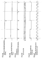
Fig. 1 shows the drive waveform process of the first
embodiment;
Fig. 2 shows the drive waveform process of the second
embodiment;
Fig. 3 is a mimetic diagram showing the light emission
display area in the PDP unit of the second embodiment;
Fig. 4 shows types of signal waveforms inputted into a
PDP driving unit, and the signal waveforms generated by the
pulse control apparatus in the second embodiment;
Fig. 5 shows the formation process of the light emission
display area of the second embodiment;
Fig. 6 shows the drive waveform process of the third
embodiment;
Fig. 7 shows a drive waveform process (variation) of the
third embodiment;
Fig. 8 shows a drive waveform process (variation) of the
third embodiment;
Fig. 9 shows a drive waveform process (variation) of the
third embodiment;
Fig. 10 shows a variation of the drive waveform process
of the present invention;
Fig. 11 shows the relationship between weights and
gradation in a conventional PDP;
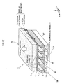
Fig. 12 is a cross-sectional perspective drawing of the
structure of the PDP unit;
Fig. 13 is a mimetic diagram showing the alignment of
the display electrodes and the address electrodes;
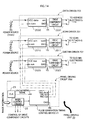
Fig. 14 is a drawing showing the structure of a PDP
driving circuit;
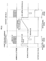
Fig. 15 is a drawing showing a drive waveform process
of a conventional PDP unit; and
Fig. 16 is a drawing showing a structure of subfields
within a frame (field).
Preferred Mode for Carrying out the Invention
<First Embodiment>
1-1. Structure of the PDP
The PDP of the present first embodiment is made up of
a PDP unit 1, and a panel driving unit 20 which drives the PDP
unit 1.
Fig. 12 is a partial and cross-sectional perspective
drawing of the main structure of an AC surface discharge PDP
unit of the first embodiment. In the drawing, a vertical
direction z corresponds to a PDP thickness direction, and
horizontal directions x and y correspond to a plane which is
parallel to the PDP unit panel surface. As shown in the drawing,
the PDP unit 1 is made up of a front panel FP and a back panel
BP which are arranged with their main surfaces facing each
other.
A plurality of pairs of display electrodes 4 and 5 (scan
electrodes 4 and sustain electrode 5) are arranged lengthwise
along the x direction on the main surface of a front glass panel
2, which is the substrate of the front panel FP, and surface
discharge is performed between the scan and sustain electrodes
of each display electrode pair. Here, as an example the display
electrodes 4 and 5 are metal electrodes formed by mixing glass
with Ag and baking the mixture, however a structure wherein
a bus line is applied onto transparent electrodes made of ITO
bandings may also be used.
Each scan electrode 4 is independently supplied with
electrical charge. Further, all of the sustain electrodes 5
are connected so as to be charged with the same electrical
potential.
The main surface of the front glass panel 2, which has
the display electrodes 4 and 5 arranged thereon, is coated with
a dielectric layer 6 made of insulative glass material, and
a protective layer 7 made of magnesium oxide (MgO) in the stated
order.
A plurality of address electrodes 11 are aligned
lengthwise in the y direction in a stripe configuration with
fixed intervals between the electrodes, on the main surface
of a back glass panel 3, which is the substrate of the back
panel BP. The address electrodes 11 are made by mixing Ag with
glass, then baking the mixture.
The main surface of the back glass panel 3 which has
address electrodes 11 arranged thereon is coated with a
dielectric layer 10 made of insulative material. Barrier ribs
8 are arranged on the dielectric layer 10 in line with the gaps
between pairs of adjacent address electrodes 11. Then, phosphor
layers 9R, 9G, and 9B, which each correspond to one of red (R),
green (G), and blue (B), are formed on the side walls of the
barrier ribs 8, and on the surface of the dielectric layer 10
between the barrier ribs 8.
Note that the drawing shows that the phosphor layers 9R,
9G, and 9B have the same width in the x direction, however a
phosphor layer of a specific color may have a larger width in
the x direction in order to balance the luminance of the
phosphor layers.
The front panel FP and the back panel BP which have the
abovementioned structure are made to face each other so that
the lengthwise directions of address electrodes 11 are
perpendicular to the display electrodes 4 and 5.
A sealing member that includes a glass having a low melting
point such as flit glass is used to seal the peripheries of
the front panel FP and the back panel BP so as to enclose the
interior section between the panels FP and BP.
In the interior section between the front panel FP and
back panel BP which have been sealed in this way, a discharge
gas (enclosed gas) which has a composition including a rare
gas such as Xe is enclosed at a given pressure (usually
approximately 40kPa-66.5kPa).
By this process, a space between the front panel FP and
the back panel BP which is partitioned by the protective layer
7, the phosphor layers 9R, 9G and 9B and pairs of adjacent
barrier ribs, forms a discharge space 12. Further, the area
in which the co-adjacent pair of display electrodes 4 and 5
and an address electrode 11 are on opposite sides of the
discharge space 12, makes up a cell (not shown in drawing) which
is used in image display. Here, Fig. 13 shows a matrix formed
by a plurality of pairs of PDP unit display electrodes 4 and
5 (rows N) and a plurality of PDP unit address electrodes 11
(lines M).
When the PDP is being driven, discharge is commenced in
each cell between the address electrode 11 and one of the
display electrodes 4 and 5, or between the display electrodes
themselves. Then discharge between the pair of display
electrodes 4 and 5 generates a short wavelength ultra violet
ray (Xe resonance line, approximate wavelength 147nm) , and the
phosphor layers 9R, 9G, and 9B receive the ultraviolet light
and emit visible light.
Next, the structure of the panel driving unit for driving
the PDP unit will be explained. Fig. 14 is a structural drawing
of the panel driving unit.
The panel driving unit 20 shown in the drawing is made
up of an address driver 203 that is connected to each address
electrode 11, a scan driver 201 that is connected to each scan
electrode 4, a sustain driver 202 that is connected to each
sustain electrode 5, and a panel driving circuit 200 that
controls the drivers 201-203, and the like.
The panel driving circuit 200 is inbuilt with a sustain
pulse generation timing control device 21, a main control
circuit 22, a clock circuit 23 and the like.
The clock circuit 23 is inbuilt with a clock (CLK)
generating unit and a PLL (Phase Locked Loop) circuit, and
generates a designated sampling clock, namely a
synchronization signal, and sends the synchronization signal
to the main control circuit 22 and the pulse control device
21.
The main control circuit 22 is inbuilt with a memory unit
which is a frame memory for storing image data inputted from
an external unit of the PDP unit 10 for a fixed period, and
a plurality of image processing circuits (not shown in drawing)
for successively extracting stored image data and performing
image processing such as gamma correction processing. The
synchronization signal generated by the clock circuit 23 is
sent to the main control circuit 22, where image information
is accepted and processed using various image processing, based
on the synchronization signal. Image data which has been
processed is sent to drive component circuits 2011, 2021, and
2031 in the drivers 201-203. The main control circuit 22
additionally performs control of the drive component circuits
2011, 2021, and 2031.
The pulse control device 21 controls the timing of pulse
generation, and is inbuilt with a commonly-known sequence
controller and microcomputer. The pulse control device 21 sends
pulses which are based on the sequence of the drive waveform
process such as initialization pulses, scan pulses, write
pulses, sustain pulses, and erase pulses (TRG scn, TRG sus,
TRG data) to the scan driver 201, the sustain driver 202 and
the address driver 203 using a designated timing for each
respective driver, according to the synchronization signal of
the clock circuit 23, and the control program of the
microcomputer. By this process, pulse voltages having are
applied to display electrodes 4 and 5 and address electrodes
11, to perform screen display.
The waveforms and output timings of the pulses based
on the sequence of the drive waveform process are controlled
by the microcomputer. The drive waveform process sequence is
formed in the microcomputer within the pulse control device
21, by processing the image-processed image data which has been
sent from the main control circuit 22.
The scan driver 201, the sustain driver 202, and the
address driver 203 are each constructed from an ordinary driver
IC (for example data driver; NEC µ PD16306A/B, and scan driver;
TI SN755854 can be used), and pulse output devices 2010, 2020,
and 2030, and respective drive element circuits 2011, 2021,
and 2031, are provided within the drivers.
The pulse output devices 2010, 2020, and 2030 are each
connected to a separate external high voltage power source from
which power is transmitted. The pulse output devices output
a designated voltage obtained from the high voltage power
source (VCC scn, VCC sus, VCC data) to the drive component
circuits 2011, 2021 and 2031 (out X, out Y, out), based on the
pulses sent from the pulse control device 21 (in scn, in sus,
in data).
1-2. Basic drive waveform process
Next, the basic drive waveform process of a conventional
PDP will be explained. Note that details of a drive waveform
process of an ordinary PDP display device are disclosed in
Japanese Laid-open Patent Publication No. 6-186927 and
Japanese Laid-open Patent Publication No. 5-307935.
As shown in Fig. 15, in a subfield, the drive waveform
process of the PDP sequentially passes through an
initialization period, a write period, a sustain period, and
an erase period.
During driving, first, in the initialization period of
the subfield, an initialization pulse is applied to the scan
electrode 4, and a cell wall charge is initialized.
Next, in the write period, a scan pulse and a write pulse
are respectively applied to the scan electrode 4 and sustain
electrode 5 which have the greatest value in the y direction
(highest position in the PDP unit), and write discharge is
performed. This process causes the wall charge to accumulate
on the surface of the dielectric layer 6 corresponding to the
scan electrode 4 and sustain electrode 5, in each cell. In a
similar fashion, a scan pulse and a write pulse are respectively
applied to the second and succeeding scan electrodes 4 and
sustain electrodes 5, and a wall charge accumulates on the
surface of the dielectric layer 6 corresponding to each cell.
By performing these pulse applications for all of the display
electrodes 4 and 5 which are arranged on the front panel FP,
one screen of a latent image is written.
Next, in the sustain period, the address electrode 11
is earthed, and a sustain pulse is applied to the scan electrode
4 and the sustain electrode 5 in an alternating fashion. In
a display cell selected by the write pulse in this way, the
electric potential of the surface of the dielectric layer 6
exceeds the discharge initializing voltage (Vf), and a sustain
discharge is generated in the gap between the pair of display
electrodes 4 and 5. A short wavelength ultraviolet ray is
generated by the sustain discharge (Xe resonance line of
approximate wavelength 147nm), and the phosphor layers 9R, 9G
and 9B are excited by the ultraviolet ray, causing visible light
to be generated, so that image display can be performed. The
image display is constructed having 60 frame/sec
(approximately 16.67ms/frame), according to a uniform
manufacturers' standard.
One frame is made up of eight subfields, and the relative
luminance ratios of the subfields are basically assigned binary
weights in ascending order of 1, 2, 4, 8, 16, 32, 64, 128. In
this explanation a subfield having a write period, a sustain
period and an erase period is presented, however in one actual
frame, it is predetermined that at least one subfield, in which
the relative luminance ratio corresponds to the lowest weight,
has only a write period and a sustain period. Further, a
subfield corresponding to the weight of level 0 gradation
display is made up of only an initialization period and a write
period (without scan pulses).
In the erase period, a narrow erase pulse is applied
to the sustain electrode 5, to extinguish the wall charge in
the cell and extinguish the image.
1-3. Properties and effects of the first embodiment
Here, the table of Fig. 11 shows display luminance, and
the weights of each relative luminance ratio in a frame
corresponding to the presence or absence of a write period and
a sustain period in subfields, during low level gradation
display (level 0 gradation - level 8 gradation) in a
conventional display device. In the table, the sections showing
"1" are subfields in which write and sustain discharge are
performed. The PDP unit used here is a 13 inch VGA standard
PDP unit, however if using a PDP unit of a different size there
will be some differences in the determined figures. However,
it may be considered that the following properties will appear
unchanged.
As shown in the table, because the luminance is 0.15cd/m2
and only an initializing discharge is generated during the
level 0 gradation display, it can be seen that the luminance
emitted by the initializing discharge is 0.15cd/m2. Further,
because there is a difference of 4 in the number of sustain
pulses during level 1 gradation display (3 sustain pulses) and
during level 2 gradation display (7 sustain pulses), and the
luminance ratio is 1.8cd/m2 , it can be seen that the luminance
emitted per sustain discharge is 0.45cd/m2. Further, because
the arithmetical ratio of luminance during level 0 gradation
display and luminance during level 1 gradation display is
2.33cd/m2, the luminance emitted by the write discharge is
calculated to be approximately 1.0cd/m2.
In this kind of ordinary PDP, the arithmetical ratio
of luminance of level 0 gradation display and level 1 gradation
display is 2.33cd/m2, and when comparing this ratio with the
ratio in CRT being approximately 0cd/m2, it can be seen that
ordinary PDP display devices have properties wherein
transitions in luminance during low level gradation display
cannot be displayed as smoothly as in CRTs.
In response to this, even if gradation display time
is falsely attempted using error diffusion processing (dither
method), because the gradation is originally low, error
diffusion noise would be noticeable, and rather than an
effective error diffusion result being gained, a new problem
of deterioration in picture quality would arise.
Therefore, as a result of diligent investigation by the
present inventors, with an aim that emission luminance of
1.2cd/ m2 can be obtained from the initialization pulse and
the write discharge, a subfield in which the relative luminance
ratio corresponds to the lowest weight in the frame was formed
having only 2 periods, the 2 periods being an initialization
period and a write period. Unlike the conventional structure,
in this subfield sustain pulses are not applied to the display
electrodes 4 and 5.
Here the initialization pulse, write pulse, scan pulse,
and voltage applied to the sustain electrode in the write period
are set at values of 400V, 70V, -70V, and 200V respectively.
The values of each of the above pulses can be substantially
the same as the conventional values. Note that the values in
the following preferred embodiment are also set as the same
as the values stated above.
With the drive waveform process described above, in a
subfield in which the relative luminance ratio corresponds to
the lowest weight, it is possible to reduce the conventional
relative luminance ratio of 2.33cd/m2 by approximately half,
to approximately 1.2cd/m2 (the total of light emission from
the initialization pulse and the write pulse), thus a dark light
emission display which is closer to 0cd/m2 can be performed.
Accordingly, during the low gradation display of the first
embodiment, a gradation display which is nearly as smooth as
in a CRT is realized, without having to use error diffusion
processing.
Further, in the first embodiment, an erase period is
unnecessary in the subfield in which the relative luminance
ratio corresponds to the lowest weight, as sustain pulses are
not applied. Accordingly, there is no light emission caused
by an erase pulse. Therefore, as shown in Fig. 1, because
transition to the initialization period of the next subfield
can be made straight after the write period, it is possible
to shorten the driving time. This is convenient in a case where
the widths of pulses, for example initialization pulses, write
pulses, and scan pulses are set.
Further, conventionally, when performing error
diffusion processing on the level 0 gradation display and the
level 1 gradation display, a tendency for error diffusion noise
to brighten and cause deterioration (graininess) of picture
quality is observed. However, in the first embodiment, because
the emission luminance of the subfield in which the relative
luminance ratio corresponds to the lowest weight is much lower
than the conventional emission luminance, noise is not
noticable, even if error diffusion processing is performed.
<Second Embodiment>
Fig. 2 is a drawing which shows subfields of the second
embodiment during low gradation display.
In the second embodiment, one frame has a drive waveform
process in which two consecutive subfields of the eight
subfields with different assigned weights each consist of an
initialization period and a write period, in a similar fashion
to the first embodiment.
Further, in a subfield 2 (the latter of the two subfields) ,
discharge is performed in the initialization period and the
write period, in a similar fashion to the first embodiment.
On the other hand, in the preceding subfield 1 of a certain
frame, in a low-level gradation display area in which the
relative luminance ratio corresponds to the lowest weight,
every second cell of a group of adjacent cells is illuminated,
as shown in Fig. 3(a). Then, in the frame which follows after
the subfield 2, the cells which were not illuminated in the
previous low-level gradation display area are illuminated, as
shown in Fig. 3(b). That is to say in the second embodiment,
illumination of the display area of the subfield in which the
relative luminance ratio corresponds to the lowest weight is
shared between two consecutive frames.
The following method is presented as a specific method
of illuminating cells as described above.
A "vertical synchronization signal (a)", a "horizontal
synchronization signal (c)", and a "clock circuit 23
synchronization signal (data clock) (d)", which are shown in
Fig. 4, act as signals which control an image. When the panel
driving unit 20 takes the signals (a), (c) and (d) from an
external device, and forms signals which invert when the (a),
(c) and (d) signals change from L level to H level in the pulse
control device 21, signals which invert each field (b) , signals
which invert each line (e), and signals which invert each
horizontal dot (cell) (f), are formed.
Of these signals, the signals which invert each line (e)
are reset by the vertical synchronization signal (a), and the
signals which invert each dot (f) are reset by the horizontal
synchronization signal (c). In this case, " being reset" refers
to being forcedly set at the L level or the H level at
synchronization signal times. An example is shown in the
drawing where signals are set at the H level at the
synchronization signal times.
When an exclusive OR of the signals which invert each
line (e) , and the signals which invert each horizontal dot are
taken, a checked pattern as shown in Fig. 5 is created. Further,
when exclusive disjunction of the checked pattern signal and
the signal which inverts per field (b) is taken, a checked
pattern signal which inverts per field is created. That is to
say, the display area image data of the subfield in which the
relative luminance ratio corresponds to the lowest weight, of
the image data inputted from an external device according to
signals inverting each field (b), each line (e), or each
horizontal dot (cell) (f), is stored as pieces of
checked-pattern image data in the memory of the PDP driving
unit in order, and used in display.
In this way, in the second embodiment, as shown in Fig.
5, a logical AND of data of a subfield and a checked pattern
made up of "0" and "1" is taken and the resulting display area
is illuminated. At this time, the "0"s and "1"s of the checked
pattern invert each field. This process enables false display
with a luminance which is half of the conventionally emitted
luminance.
Note that in subfield 2, logical AND of a checked pattern
is not taken.
According to the abovementioned second embodiment, in the
display area of the subfield in which the relative luminance
ratio corresponds to the lowest weight, when comparing emission
luminance of the display area in which adjacent cells appear
to be illuminated alternately in a checked pattern every frame,
to full illumination (that is, by the emission luminance in
the subfield 2), the light emission of the initialization
pulses is equal, although the light emitted by the write pulse
can be decreased by half. That is to say, in the second
embodiment, it is possible to keep the total emission luminance
of the subfield 1, in which the lowest relative luminance ratio
corresponds to the lowest weight, at approximately 0.65cd/m2,
being the total of the emission luminance of the initialization
pulse (0.15cd/m2) and the emission luminance of the write
discharge (approximately 0.5cd/m2), which is half of
(1.0cd/m2). This total, being as low as 1/4 of the 2.33cd/m2
emission luminance of a conventional gradation display which
was mentioned previously, shows that the second embodiment has
superior low gradation display performance.
Further, in the second embodiment, because the emission
luminance in subfield 2 is also kept low at approximately
1.2cd/m2, a plurality of dark, low gradations which are nearer
to 0cd/m2 can be displayed in both subfields 1 and 2.
If error diffusion process is combined with the second
embodiment, the error diffusion noise will be barely noticed,
and deterioration of the picture quality can be kept to a
minimum.
Note that here an example was shown wherein the
illumination of adjacent cells in a display area of subfield
1 alternates in consecutive frames, however as the second
embodiment is not limited to this driving method, a driving
method in which cells are divided into cell groups of several
cells, and the illumination of the cell groups alternates in
consecutive frames may also be used. However, because the
picture in the display area is blurred when cell groups are
formed having very large numbers of cells, caution is required
particularly for the formation of cell groups in a case where
the PDP unit 1 is a high definition PDP, such as a high vision
PDP.
Further, in the second embodiment, an example is shown
combining each of the drive waveform processes of subfield 1
and subfield 2, which are characteristic of the present
invention. However, as the present invention is not limited
to a drive waveform process which combines subfield 1 and
subfield 2, subfield 1 may be combined with a subfield of the
conventional structure instead of subfield 2.
Further, subfield 1 has a structure in which the
illumination of adjacent cells in the display area of subfield
1 alternates in two consecutive frames. However, as the present
invention is not limited to a case where adjacent cells
illuminate alternately, illumination of every second cell, or
of every third cell or every greater number of cells, may also
be performed, in all of the corresponding display areas of the
total of the plurality of consecutive frames. If illumination
of cells is performed in this way, the number of illuminated
cells per subfield 1 can be reduced to a fraction of the
conventional number, therefore enabling even darker display.
<Third Embodiment>
Fig. 6 is a drawing showing a subfield during low
gradation display in the second embodiment.
In the drive waveform process of the third embodiment which
is shown in the drawing, firstly, as in the first embodiment,
the subfield in which the relative luminance ratio corresponds
to the lowest weight consists of two periods, the two periods
being the initialization period and the write period. The drive
waveform process of the third embodiment also has a
characteristic wherein an initialization pulse, which has an
inclined accelerating section, is applied in the
initialization period of the subfield following after the
abovementioned subfield. Concerning the specific incline of
the accelerating section, from actual results determined by
the present inventors, a maximum incline of approximately
7.5V/µs is considered possible, though it is preferred that
the incline be in a range of 1V/µs- 3.5V/µs. The maximum value
of the initialization pulse may be approximately 400V, which
is the conventional maximum value.
Generation of erroneous discharge (of for example
0.5cd/m2), which occurs when the wall charge originating from
the discharge generated in the subfield in which the relative
luminance ratio corresponds to the lowest weight is brought
into the next subfield (especially the wall charge generated
by the write discharge in the write period), is effectively
prevented in this kind of drive waveform process which applies
an initialization pulse having an accelerating section. That
is to say, in the third embodiment, because the wall charge
remaining in a cell from the previous subfield is gradually
initialized by the initialization pulse 400 having an inclined
accelerating section, and the electric potential between the
display electrodes 4 and 5, or between the display electrodes
4 and 5 and the address electrode 11 decreases, occurrence of
spasmodic discharge is avoided. Accordingly, in the subfield
in which the relative luminance ratio corresponds to the lowest
weight, and the next consecutive subfield, the occurrence of
bright erroneous discharge which is undesirable for image
display, and the carrying over of the erroneous discharge into
the sustain period, can be effectively avoided, thus enabling
good quality low gradation display.
Note that as the initialization pulse having an
accelerating section is not limited to the pattern of the
abovementioned inclined initialization pulse 400, an
initialization pulse such as an initialization pulse 500 having
a curved accelerating section shown in Fig. 7 may also be used.
In the case of the initialization pulse 500 shown in the drawing,
the wall charge in the cell is smoothly initialized by the
initialization pulse 500 based on a gradually accelerating
curve using the curve function expressed as f(x)={1-(1/e)x}1/2,
without causing any noticeable erroneous discharge.
Further, other than the above function, the gradually
accelerating section curve may be formed based on a
trigonometric function such as a sine waveform, (sin curve)
or a cosine waveform (cos curve), or a type of exponential
function or high-order function. However it is preferable to
actually verify whether or not the occurrence of noticeable
erroneous discharge is effectively prevented by the
accelerating section having an arbitrary curve, using an
oscilloscope or a microscope for discharge verification.
Note that it is possible that the accelerating section
has a form in which the initialization pulse is steeply raised
(raised by 150V in this case) in a range in which erroneous
discharge will not occur, as shown in a pulse waveform 600 of
Fig. 8 and an exponential function waveform 700 of Fig. 9. The
initialization pulse being raised in such a way allows the width
of the initialization pulse to be reduced to a certain extent,
therefore being advantageous in enabling a reduction in
the driving time.
<Other Items>
The drive waveform process of the present invention may
be formed from differential waveforms, by applying pulses of
suitable voltages to both the scan electrode 4 and the sustain
electrode 5 in a subfield. Here in the drive waveform process
of Fig. 10, the initialization pulse (differential waveform
400) is made up of the total of 200V applied to the scan
electrode 4, and -200V applied to the sustain electrode 5. In
a similar fashion, the scan pulse, write pulse, and the
initialization pulse having an accelerating section shown in
the third embodiment, may also be made up of differential
waveforms. When differential waveforms such as those
described above make up these pulses, the individual voltages
to be applied when each of the scan driver 201, the sustain
driver 202 and the address driver 203 are supplied with
electricity are lowered, therefore the use of a highly
voltage-resistant driver IC is unnecessary, and the use of such
waveforms can be expected to have a cost-wise advantage.
Note that during PDP driving time there may also be cases
where the total of 256 gradations are expressed by each frame
being made up of 12 subfields, rather than eight subfields as
in the previous example. In this case the weights of each
subfield are assigned in an ascending order such as 1, 2, 4,
6, 10, 14, 19, 26, 33, 47, 53. This is the same as in the case
of one field made up of eight subfields for gradations 0 to
7, however the eighth gradation illuminates the subfields 2
and 4. By further changing the assigned weights, a display of
512 gradation or higher is made possible. This kind of frame
structure may also be applied to the present invention.
Industrial Applicability
The present invention can be applied to PDPs used in
display devices of information terminal devices and computers,
and television image display devices.