EP1417757B1 - Systeme und verfahren zur impulsbreitenmodulation - Google Patents
Systeme und verfahren zur impulsbreitenmodulation Download PDFInfo
- Publication number
- EP1417757B1 EP1417757B1 EP02773192A EP02773192A EP1417757B1 EP 1417757 B1 EP1417757 B1 EP 1417757B1 EP 02773192 A EP02773192 A EP 02773192A EP 02773192 A EP02773192 A EP 02773192A EP 1417757 B1 EP1417757 B1 EP 1417757B1
- Authority
- EP
- European Patent Office
- Prior art keywords
- pulse width
- signal
- width modulated
- generating
- output
- Prior art date
- Legal status (The legal status is an assumption and is not a legal conclusion. Google has not performed a legal analysis and makes no representation as to the accuracy of the status listed.)
- Expired - Lifetime
Links
Images


Classifications
-
- H—ELECTRICITY
- H03—ELECTRONIC CIRCUITRY
- H03F—AMPLIFIERS
- H03F3/00—Amplifiers with only discharge tubes or only semiconductor devices as amplifying elements
- H03F3/20—Power amplifiers, e.g. Class B amplifiers, Class C amplifiers
- H03F3/21—Power amplifiers, e.g. Class B amplifiers, Class C amplifiers with semiconductor devices only
- H03F3/217—Class D power amplifiers; Switching amplifiers
-
- H—ELECTRICITY
- H02—GENERATION; CONVERSION OR DISTRIBUTION OF ELECTRIC POWER
- H02M—APPARATUS FOR CONVERSION BETWEEN AC AND AC, BETWEEN AC AND DC, OR BETWEEN DC AND DC, AND FOR USE WITH MAINS OR SIMILAR POWER SUPPLY SYSTEMS; CONVERSION OF DC OR AC INPUT POWER INTO SURGE OUTPUT POWER; CONTROL OR REGULATION THEREOF
- H02M7/00—Conversion of AC power input into DC power output; Conversion of DC power input into AC power output
- H02M7/42—Conversion of DC power input into AC power output without possibility of reversal
- H02M7/44—Conversion of DC power input into AC power output without possibility of reversal by static converters
- H02M7/48—Conversion of DC power input into AC power output without possibility of reversal by static converters using discharge tubes with control electrode or semiconductor devices with control electrode
- H02M7/53—Conversion of DC power input into AC power output without possibility of reversal by static converters using discharge tubes with control electrode or semiconductor devices with control electrode using devices of a triode or transistor type requiring continuous application of a control signal
- H02M7/537—Conversion of DC power input into AC power output without possibility of reversal by static converters using discharge tubes with control electrode or semiconductor devices with control electrode using devices of a triode or transistor type requiring continuous application of a control signal using semiconductor devices only, e.g. single switched pulse inverters
- H02M7/539—Conversion of DC power input into AC power output without possibility of reversal by static converters using discharge tubes with control electrode or semiconductor devices with control electrode using devices of a triode or transistor type requiring continuous application of a control signal using semiconductor devices only, e.g. single switched pulse inverters with automatic control of output wave form or frequency
- H02M7/5395—Conversion of DC power input into AC power output without possibility of reversal by static converters using discharge tubes with control electrode or semiconductor devices with control electrode using devices of a triode or transistor type requiring continuous application of a control signal using semiconductor devices only, e.g. single switched pulse inverters with automatic control of output wave form or frequency by pulse-width modulation
-
- H—ELECTRICITY
- H03—ELECTRONIC CIRCUITRY
- H03F—AMPLIFIERS
- H03F3/00—Amplifiers with only discharge tubes or only semiconductor devices as amplifying elements
- H03F3/20—Power amplifiers, e.g. Class B amplifiers, Class C amplifiers
- H03F3/21—Power amplifiers, e.g. Class B amplifiers, Class C amplifiers with semiconductor devices only
- H03F3/217—Class D power amplifiers; Switching amplifiers
- H03F3/2173—Class D power amplifiers; Switching amplifiers of the bridge type
-
- H—ELECTRICITY
- H03—ELECTRONIC CIRCUITRY
- H03K—PULSE TECHNIQUE
- H03K7/00—Modulating pulses with a continuously-variable modulating signal
- H03K7/08—Duration or width modulation ; Duty cycle modulation
-
- H—ELECTRICITY
- H03—ELECTRONIC CIRCUITRY
- H03F—AMPLIFIERS
- H03F2200/00—Indexing scheme relating to amplifiers
- H03F2200/351—Pulse width modulation being used in an amplifying circuit
Definitions
- the present invention relates, in general, to pulse width modulation ("PWM”) methods and systems.
- PWM pulse width modulation
- a PWM (pulse width modulated) signal is one in which the information is contained in the width of each pulse, typically of a repeating string of pulses. It may be considered a form of analog signal in that the information is contained in the time duration of a pulse, which is varied continuously, or in such small steps as to be effectively continuous. That is to be contrasted with a digital signal in which information is contained in discrete steps (such as two steps for binary) and in which values are assigned to the various discrete combinational possibilities.
- PWM pulse width modulation
- inverters DC to AC converters
- PWM control may be used to control inverters in any of a variety of inverter applications, with examples including power supply applications such as uninterruptible power supplies and the like, alternative energy applications such as fuel cells, motor drives, audio amplifiers, and the like.
- PWM signals There are many known methods for creating PWM signals.
- Conventional PWM sequences may be generated by comparing a triangle or ramp carrier with a modulating function.
- signals are created that contain both high-frequency switching energy and low frequency waveform energy.
- the low frequency content limits the overall PWM applications.
- Inverters for motor drives for example, can be complicated systems that must reconstruct gate drive waveforms and deliver power without transformer coupling. The desire to avoid transformers has hampered development of a "general purpose inverter.”
- multi-level inverters which use several different dc input voltages to produce a waveform that tracks a modulating signal more closely than conventional two-level and three-level inverters. They are common in high-voltage applications, since the switches in them act in series. It is generally known that the control signals for multi-level inverters can be generated through a multiple-carrier PWM process. In such systems, the triangle carrier is shifted up or down to form a set of carriers corresponding to each output level. This approach, however, does not support high-frequency links or provide a way to simplify the inverter system itself. It intended solely to facilitate the use of many switches in a series configuration. Further descriptions of such systems may be found, by way of example, in, " A new multilevel PWM method: a theoretical analysis,” Carrara et al., IEEE Trans. Power Electronics, vol. 7, pp. 497-505 (1992 ).
- US 4,782,398 relates an image processing apparatus of which has a look-up-table (LUT) for generating an image signal, a first pattern signal generator for generating a first pattern signal, a comparator for processing the image signal using the first pattern signal and outputting a first pulse width modulation signal, a second pattern signal generator for generating a second pattern signal different from the first pattern signal, another comparator for processing the image signal using the second pattern signal and outputting a second pulse width modulation signal, and an OR gate for synthesizing the first and second pulse width modulation signals.
- LUT look-up-table
- US 5,886,586 relates to a PWM modulator, which employs one or more integrators with reset stages, which can be generally applied to implement feed-forward control of a family of converters, current mode control with linear or non linear compensating slope, and a family of unity-power-factor rectifiers at continuous or discontinuous conduction mode.
- a method of the invention has the steps of segmenting a base carrier waveform into a plurality of carrier waveforms, and providing at least one modulating signal.
- the plurality of carrier waveforms are compared to the at least one modulating signal to produce a plurality of comparator outputs, which are then mathematically combined to produce a pulse width modulated control signal.
- this pulse width modulated control signal is then convolved with a clock signal to produce a final pulse width modulated output.
- An exemplary system of the invention for generating a gate drive sequence includes a segmenter operative to segment a base carrier waveform into a plurality of carrier waveforms, and a plurality of comparators linked to the segmenter and also linked to at least one modulating signal.
- the plurality of comparators are operative to compare the plurality of carrier waveforms to the at least one modulating signal.
- a mathematical operator is further provided that is linked to each of the comparators and operative to output the gate drive sequence defined through mathematical combination of the plurality of
- a switching circuit is additionally provided.
- the gate control sequence and a square wave signal are input to the switching circuit, which uses the signals to produce a pulse width modulated output.
- Methods and systems of the invention solve many otherwise unresolved problems of the prior art and provide valuable advantages. For example, through practice of multiple-carrier PWM methods and systems of the invention, relatively low cost and low complexity inverter designs can be achieved that support transformer isolation and offer other advantages. It is also possible to combine more than one modulating signal into a single output that entails independent PWM of each modulating signal.
- FIG. 1 is useful in illustrating an exemplary method of the invention for generating a PWM output.
- FIG. 1(a) illustrates a square wave clock signal
- FIG. 1 (b) illustrates a base carrier waveform in the general form of a triangle carrier.
- a method of the invention segments the triangle shaped base carrier waveform on a time basis into a rising portion carrier waveform, shown in FIG. 1(c) , and into a falling portion carrier waveform shown in FIG. 1(d) .
- the result of performing a step of comparing the rising portion waveform of FIG. 1(c) to a modulating function in a comparator is graphically shown in FIG. 1(e) , and the result of a step of comparing the falling portion waveform of FIG.
- FIG. 1(g) shows the result of adding the outputs of the comparisons graphically represented in FIG. 1(e) and 1(f) .
- the resultant waveform of FIG. 1(g) preserves the information originally present in the carrier waveform of FIG. 1(b) .
- This PWM signal may be used to control any of a variety of controls, and accordingly may be referred to as a "gate control sequence.”
- the inverter output graphically shown in FIG. 1(i) is a conventional PWM signal.
- each switching device used in processing the various waveforms is controlled with a square wave of duty ratio approximately 50%, while the relative timing of the two square waves yields the final PWM output.
- Methods of the invention may be practiced using other forms of base carriers, with an example including, but not limited to, sawtooth waveforms that are always rising. Also, those knowledgeable in the art will appreciate that other steps of segmenting the base carrier waveform other than based on time may be practiced. For example, segmenting may be practiced based on high and low voltage levels, phase shifting, and the like.
- a triangle base carrier waveform for instance, may be of a sawtooth form that is then segmented into a high portion and a low portion based on voltage level. It will be appreciated that use of these carrier waveforms in practice of the invention will yield similar PWM outputs, but with distinct timing properties that can be exploited in useful ways.
- the square waveform PWM output of FIG. 1(i) for instance, always displays phase-leading behavior relative to the original square wave clock.
- FIG. 2 illustrates an alternative to FIG. 1 .
- a clock signal is shown in FIGS. 2(a) and (h) .
- the base carrier waveform of FIG. 2(b) is consistent with that of FIG. 1(b) , as are the segmented falling and rising carrier waveforms of FIGS. 2(c) and 2(d) .
- the order of comparison is changed with respect to FIG. 1 , however, with the falling portion waveform of FIG. 2(d) compared to the modulating function as graphically represented in FIG. 2(e) , and the rising portion waveform of FIG. 2(c) compared to the negative of the modulating function as graphically shown in FIG. 2(f) .
- This change of comparison order results in the output PWM signal of FIG.
- phase-lagging behavior as opposed to the phase leading behavior shown in FIG. 1(i) .
- the combination of phase-lagging and phase-leading behavior possible through methods steps of the invention gives rise to a "cycloconverter" approach in which natural commutation switch action is possible.
- FIG. 3 is useful for illustrating an additional exemplary method of the invention.
- FIG. 3 is generally consistent with FIGS. 1 and 2 , except that an always rising base carrier waveform shown in FIG. 3(b) is segmented on a time basis into the two carrier waveforms graphically illustrated in FIGS. 3(c) and 3(d) .
- These segmented carrier waveforms are compared to the modulated signal and negative modulated signal, as is graphically illustrated by FIGS. 3(e) and 3(f) , respectively.
- the outputs of these comparisons are added to one another to result in the PWM control signal waveform illustrated in FIG. 3(g) . Convolving this signal with the clock signal of FIG. 3(h) results in the output PWM waveform shown in FIG. 3(i) .
- FIGS. 1 and 2 illustrate more preferred invention embodiments for natural commutation applications.
- FIGS. 1-3 graphically illustrate methods of the invention that segment a base carrier waveform into two carrier waveforms
- other invention embodiments may include a step of segmenting a base carrier waveform into more than two carrier waveforms.
- four or six carrier waves may be formed.
- FIGS. 1-3 illustrate method embodiments in which two modulating signals are provided.
- Other invention embodiments may include steps of using other numbers of modulating signals. It is contemplated that an invention embodiment may be of use that uses only a single modulating signal. More preferably, at least two modulating signals are provided, and four if the number of carrier waveforms is six or more.
- the frequency of the carrier waveform is normally much higher than that in the modulating signal. Higher carrier frequencies allow for easier filtering of PWM waveforms. A high carrier frequency is more suitable for transformer coupling that the modulating signal itself, since higher frequencies can be delivered with smaller magnetic devices.
- FIG. 4 is a schematic block diagram useful for illustrating an exemplary system and method of the invention for generating a gate control sequence PWM signal that may be generally similar to that illustrated by FIGS. 1(g) , 2(g) , and 3(g) ; and for producing PWM output that may be generally similar with the output PWM signals shown in FIG. 1(i) , 2(i) , and/or 3(i).
- a base carrier waveform such as a triangle or a sawtooth ramp is input to a segmenter 10 that segments the base carrier waveform on a time basis into two individual carrier waveforms, C1(T) and C2(T).
- the segmenter 10 may comprise a decommutator, phase shifter, or the like.
- suitable decommutators can be found in time-division multiplexing (TDM) communication systems.
- the segmenter 10 is operating in synchronism with the carrier clock.
- the segmentation or decommutation rate f is set to the same as the frequency as the carrier in case of a ramp waveform, or to twice the frequency in the case of a triangle waveform.
- a modulating function M1(T) is communicated to a first comparator 12 for comparing to the carrier waveform C1(T).
- the modulating function M1(T) is processed by a 180° phase-shifter 14, and the phase shifted output modulating function M2(T) is communicated to a second comparator 16 for comparison to the carrier waveform C2(T).
- Each of the comparators 12 and 16 outputs a conventional PWM sequence (P1 and P2, respectively).
- the comparator outputs P1 and P2 are combined mathematically ("combined mathematically” and like terms as used herein is intended to broadly refer to combination through mathematic operation such as addition, subtraction, or the like) at mathematical operator 18 to generate a gate drive sequence, which as those skilled in the art will appreciate consists of a pulse width modulated signal.
- the mathematical operator may comprise any of a variety of adders, subtractors, arithmetic logic units, or like elements that are generally known in the art.
- the gate control sequence is for controlling a switching circuit 20 that may be any of a variety of elements, with examples including but not limited to a transistor, a circuit or circuits, a logical switch or gate, an inverter circuit, a relay, a semi-conducting device, and the like.
- a preferred switching circuit 20 comprises a switching power converter.
- the switching circuit 20 also receives an input square wave such as a clock signal. With the right choices of phasing, gate sequences will result that operate to switch or control the switching circuit 20 against a square-wave source such as the high frequency link voltage input to produce PWM output.
- the sequences can be two-level or three-level.
- the input square wave may be of high frequency to form a high frequency (“HF") link.
- HF high frequency
- the gate control sequence should avoid low-frequency content, yet should also retain information about the modulating function.
- One way to accomplish this is to generate two sequences (e.g., P1 and P2), then subtract them to eliminate low-frequency modulation. The result is a three-level signal.
- An alternative is to modulate one sequence with a function m(t), the other with -m(t) , and then add them. The result is a two-level signal. Since the sequences are constrained to separate time windows, the combination still retains information about the underlying m(t) function, even though low-frequency content is removed.
- the gate drive sequence and the square wave are generally interchangeable with regards to the switching circuit 20. That is, either of the gate drive sequence or the square wave may be used to control the switching circuit 20, and either may be used as the power input. Different applications may make use of one or the other of the signals preferred for control of the switching circuit 20.
- Table 1 lists nine two-carrier conditions, the resulting sequences, and the ultimate equivalent PWM approach that would have generated the same output.
- the four shaded entries in Table 1 (rows 2, 5, 6 and 9) are graphically depicted in FIG. 5 as examples.
- the control sequence is "mixed" with a square wave to show the recovery of a two-level PWM signal at the converter output. All the sequences given in Table 1 are intended for HF link applications: the modulation and combination processes are selected to cancel out the carrier, either with a phase shift or by subtraction.
- the gate sequence waveforms in FIG. 5 demonstrate several advantageous aspects of exemplary multiple-carrier PWM methods and systems of the invention.
- the two-level gate sequences in FIG. 5(a) and 5(b) maintain a duty ratio of nearly 50% all the way through the cycle.
- the 50% duty ratio supports convenient transformer isolation for the gate drives. Since the pulse width has virtually no dynamic range, there are no limitations for narrow or wide pulses.
- the gate drive sequence in FIG. 5(a) is always phase-lagged relative to the HF link square-wave, while that in FIG. 5(b) always leads. Thus, unidirectional devices can be used in the output stage. If sequence (a) is used when load current is positive while (b) is used for negative load current, a complete naturally-commutated PWM cycloconverter results.
- FIG. 5(a), 5(b) and 5(c) all produce ultimate PWM outputs with an effective switching frequency double that of the switching devices - with advantages for switching losses.
- Those in FIG. 5(c) and 5(d) provide HF link gate drives, with simple rectification at the gate terminals to recover the correct signals.
- Those skilled in the art will appreciate that there are many alternatives within the scope of the invention for generating multiple-carrier PWM signals, such as the use of synchronized push-pull PWM ICs, or digital approaches.
- FIG. 6 shows an exemplary three-phase cycloconverter-type HF link inverter, which consists of an open-loop inverter to generate a 50% square wave, a HF transformer, the output converter, and passive filtering for the output. It is intended to use two-carrier PWM for natural commutation.
- the primary-side inverter bridge uses unipolar devices (MOSFETs or IGBTs with inverse diodes), while the three-phase output bridge consists of twelve unidirectional switches organized in six pairs. With natural commutation, only the leading edge of the gate pulses is needed, and the only feedback is the sign of the output current.
- FIG. 6 shows a single-phase version of FIG. 6 because control can be applied either at the input bridge or the output bridge.
- the gate sequence multiplied by the square wave, recovers a conventional PWM output.
- FIG. 7 shows a switch timing diagram for a single-phase cycloconverter-type HF link inverter. Natural commutation in the HF link circuit is not affected significantly by dead time. When a short dead time is provided for the primary-side inverter, the output cannot be quite as high, but the general operation is unaffected.
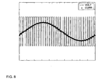
- FIG. 8 shows a simulation result for this HF link inverter, running under two-carrier PWM to provide natural commutation.
- the load frequency is 50 Hz
- the switching frequency is 1 kHz
- a passive filter designed for this output has been applied to allow easy identification of the current waveform.
- the dead-time for the primary-side inverter has been expanded to 60 millisec to make it clearly visible. It is noted that the waveforms and ripple behavior are the same as those of conventional PWM.
- the circuit diagram of FIG. 9 illustrates a system of the invention that embodies a direct way to utilize the waveforms of FIG. 1 to produce an inverter.
- the waveform PWM1 of FIG. 1(g) is used to create a square-wave voltage source of positive and negative polarity.
- the only difference between the input waveform and the signal shown in FIG. 1 (g) is that the magnitude used in FIG. 4 can be any voltage, not just 1 V.
- the four switches labeled "clock" in the bridge are operated at a fixed 50% duty - directly from the clock signal. At the output terminals, the result is conventional PWM as in FIG. 1(i) .
- FIG. 10 illustrates an additional exemplary system of the invention for creation of the source waveform of FIG. 1 from a fixed DC potential to produce a complete inverter.
- waveform PWM1(t) e.g., FIG. 1(g)
- 1 - PWM1(t) control two switches in a push-pull manner.
- the output switches operate at fixed 50% duty from the clock (or 1 - clock) to recover the desired PWM. This is then filtered in a usual way for delivery to a load.
- the waveform process can be reversed: the clock can be used for the input switches, while the PWM1(t) signal can be used for the output switches, with no fundamental change in operation.
- FIG. 11 shows an exemplary naturally-commutated circuit of the invention for inverter applications.
- the input switches operate based on the clock signal.
- the output devices use a combination of PWM1(t) (e.g., FIG. 1(g) ) and PWM2(t) (e.g., FIG. 2(g) ).
- the combination is selected in a conventional way: when the output load current is positive, the choice is made to use a waveform with only phase delay (turn-off delay) relative to the clock. When the output is positive, the choice is made to use only phase advance.
- single-sided devices such as silicon-controlled rectifiers (SCRs) can be used for output.
- SCRs silicon-controlled rectifiers
- a base carrier waveform is segmented into four carrier waveforms. These four carrier waveforms are then compared to two modulating signals to encode both signals into a single PWM gate drive sequence. The sequence is then used in conjunction with a synchronized square wave, and then with a second square wave in quadrature (1/4 cycle shift) with the first. Modulation with "Left” and "Right" signals (such as might be found in an audio application, for example) is performed as follows:
- multiple-carrier PWM of the invention in the context of a naturally-commutated HF link inverter include the ease of implementation and the simplicity of gate drive circuits. Additional more formal advantages are related to the PWM process of the invention: the output voltage waveforms can be arranged to match conventional two-level PWM signals, and prior understandings of harmonics, filter design, ripple, and other design issues can be applied directly. Multi-carrier PWM methods and systems of the invention serve as a direct way to construct HF inverter control waveforms. Resultant PWM output provides gating signals suitable for square-wave cycloconverters, for isolated gate drives, and for other implementation aspects of HF link inverters.
- Multi-carrier PWM techniques and systems of the present invention are believed to have particular promise in the implementation of low-cost inverters, as well as for HF link applications of medium power (1 kW - 20 kW).
- waveforms produced through practice of the present invention are true PWM output waveforms, rather than the phase-shifted results produced in a cycloconverter.
- the PWM signals can be designed based on any desired requirements, and can be set up to have specific frequency content or to produce a specific waveform shape.
- the control is easy to generate and couple directly into the switching devices. Methods and systems of the invention, for example, can be valuable for use with audio amplifier applications with variable signals.
Landscapes
- Engineering & Computer Science (AREA)
- Power Engineering (AREA)
- Inverter Devices (AREA)
- Amplifiers (AREA)
- Radar Systems Or Details Thereof (AREA)
- Pulse Circuits (AREA)
- Amplitude Modulation (AREA)
- Magnetic Resonance Imaging Apparatus (AREA)
Claims (28)
- Verfahren zum Erzeugen eines pulsbreitenmodulierten Steuersignals, das die folgenden Schritte beinhaltet:Erzeugen einer Basisträgerwellenform;Segmentieren der genannten Basisträgerwellenform in eine Mehrzahl von individuellen Trägerwellenformen;Erzeugen von wenigstens einem Modulationssignal;Vergleichen der genannten Mehrzahl von Trägerwellenformen mit dem genannten wenigstens einen Modulationssignal zum Erzeugen einer Mehrzahl von Komparatorausgängen; undmathematisches Kombinieren der genannten Mehrzahl von Komparatorausgängen zum Erzeugen eines pulsbreitenmodulierten Steuersignals.
- Verfahren zum Erzeugen eines pulsbreitenmodulierten Steuersignals nach Anspruch 1, wobei das Verfahren ferner zum Bereitstellen eines pulsbreitenmodulierten Ausgangs dient und ferner die folgenden Schritte beinhaltet:Eingeben eines Rechteckwellensignals in einen Schaltstromkreis; undEingeben des genannten pulsbreitenmodulierten Steuersignals in den genannten Schaltstromkreis, wobei der genannte Schaltstromkreis das genannte pulsbreitenmodulierte Steuersignal und das genannte Rechteckwellensignal zum Erzeugen des pulsbreitenmodulierten Ausgangs verwendet.
- Verfahren zum Erzeugen eines pulsbreitenmodulierten Ausgangs nach Anspruch 2, wobei das genannte pulsbreitenmodulierte Steuersignal zum Steuern des genannten Schaltstromkreises verwendet wird.
- Verfahren zum Erzeugen eines pulsbreitenmodulierten Ausgangs nach Anspruch 2, wobei das genannte Rechteckwellensignal zum Steuern des genannten Schaltstromkreises verwendet wird.
- Verfahren zum Erzeugen eines pulsbreitenmodulierten Ausgangs nach Anspruch 2, wobei der genannte Schaltstromkreis eine Inverterschaltung umfasst.
- Verfahren zum Erzeugen eines pulsbreitenmodulierten Ausgangs nach Anspruch 2, wobei der genannte Schaltstromkreis einen Schaltleistungswandler umfasst.
- Verfahren zum Erzeugen eines pulsbreitenmodulierten Ausgangs nach Anspruch 2, wobei das genannte Rechteckwellensignal ein Taktsignal umfasst.
- Verfahren zum Erzeugen eines pulsbreitenmodulierten Steuersignals nach Anspruch 1, wobei das Verfahren ferner zum Bereitstellen eines pulsbreitenmodulierten Ausgangssignals dient und ferner die folgenden Schritte beinhaltet:Falten des genannten pulsbreitenmodulierten Steuersignals mit einem Taktsignal zum Erzeugen des pulsbreitenmodulierten Ausgangs.
- Verfahren zum Erzeugen eines pulsbreitenmodulierten Steuersignals nach Anspruch 1, wobei der Schritt des mathematischen Kombinierens der genannten Mehrzahl von Komparatorausgängen das Addieren der genannten Mehrzahl von Komparatorausgängen miteinander beinhaltet.
- Verfahren zum Erzeugen eines pulsbreitenmodulierten Steuersignals nach Anspruch 1, wobei der Schritt des mathematischen Kombinierens der genannten Mehrzahl von Komparatorausgängen das Subtrahieren von einem aus der genannten Mehrzahl von Komparatorausgängen von einem anderen aus der genannten Mehrzahl von Komparatorausgängen beinhaltet.
- Verfahren zum Erzeugen eines pulsbreitenmodulierten Steuersignals nach Anspruch 1, wobei die genannte Basisträgerwellenform ansteigende und abfallende Abschnitte hat und wobei der Schritt des Segmentierens der genannten Basisträgerwellenform das Verwenden der genannten ansteigenden Abschnitte zum Definieren einer ersten Trägerwellenform und das Verwenden der genannten abfallenden Abschnitte zum Definieren einer zweiten Trägerwellenform beinhaltet.
- Verfahren zum Erzeugen eines pulsbreitenmodulierten Steuersignals nach Anspruch 1, wobei der Schritt des Segmentierens der genannten Basisträgerwellenform das Segmentieren der genannten Basisträgerwellenform auf einer Zeitbasis beinhaltet.
- Verfahren zum Erzeugen eines pulsbreitenmodulierten Steuersignals nach Anspruch 1, wobei der Schritt des Segmentierens der genannten Basisträgerwellenform entweder das Phasenverschieben der genannten Basisträgerwellenform oder das Segmentieren der genannten Basisträgerwellenform auf einer Spannungspegelbasis beinhaltet.
- Verfahren zum Erzeugen eines pulsbreitenmodulierten Steuersignals nach Anspruch 1, wobei das genannte eine Modulationssignal eine Mehrzahl von Modulationssignalen beinhaltet und wobei der Schritt des Vergleichens der genannten Mehrzahl von Trägerwellenformen mit dem genannten wenigstens einen Modulationssignal das Vergleichen einer ersten aus der genannten Mehrzahl von Trägerwellenformen mit einem ersten Modulationssignal zum Erzeugen eines ersten Komparatorausgangs und das Vergleichen einer zweiten aus der genannten Mehrzahl von Trägerwellenformen mit einem zweiten Modulationssignal zum Erzeugen eines zweiten Komparatorausgangs beinhaltet.
- Verfahren zum Erzeugen eines pulsbreitenmodulierten Steuersignals nach Anspruch 14, wobei das genannte erste modulierte Signal um 180° phasenverschoben wird, um das genannte zweite modulierte Signal zu definieren.
- Verfahren zum Erzeugen eines pulsbreitenmodulierten Steuersignals nach Anspruch 1, wobei das genannte pulsbreitenmodulierte Steuersignal ein Dreipegel-Signal ist.
- Verfahren zum Erzeugen eines pulsbreitenmodulierten Steuersignals nach Anspruch 1, wobei die genannte Mehrzahl von Trägerwellen wenigstens vier Trägerwellen umfasst.
- Verfahren zum Erzeugen eines pulsbreitenmodulierten Steuersignals nach Anspruch 1, wobei:der genannte Segmentierschritt das Segmentieren der genannten Basisträgerwellenform auf einer Zeitbasis in wenigstens eine erste Trägerwellenform und eine zweite Trägerwellenform beinhaltet;der genannte Bereitstellungsschritt das Erzeugen eines ersten Modulationssignals beinhaltet;der genannte Vergleichsschritt das Vergleichen der genannten ersten Trägerwellenform mit dem genannten ersten Modulationssignal zum Bereitstellen eines ersten Komparatorausgangs beinhaltet;der genannte Bereitstellungsschritt ferner das Phasenverschieben des genannten ersten Modulationssignals zum Definieren eines zweiten Modulationssignals beinhaltet;der genannte Vergleichsschritt ferner das Vergleichen der genannten zweiten Trägerwellenform mit dem genannten zweiten Modulationssignal zum Bereitstellen eines zweiten Komparatorausgangs beinhaltet;der genannte Schritt des mathematischen Kombinierens das mathematische Kombinieren des genannten ersten Komparatorausgangs mit dem genannten zweiten Komparatorausgang zum Erzeugen einer Toransteuerungssequenz beinhaltet; und wobei das Verfahren ferner die folgenden Schritte beinhaltet:Eingeben eines Rechteckwellen-Leistungssignals in einen Leistungswandlungsschaltstromkreis; undSteuern des genannten Leistungswandlungsschaltstromkreises mit der genannten Toransteuerungssequenz, so dass der genannte Leistungswandlungsschaltstromkreis den pulsbreitenmodulierten Ausgang ausgibt.
- System zum Erzeugen einer Toransteuerungssequenz, das Folgendes umfasst:einen Segmentierer (10) zum Segmentieren einer Basisträgerwellenform in eine Mehrzahl von Trägerwellenformen;eine Mehrzahl von Komparatoren (12, 16), die mit dem genannten Segmentierer und mit wenigstens einem Modulationssignal verknüpft sind, wobei die genannte Mehrzahl von Komparatoren die Aufgabe hat, die genannte Mehrzahl von Trägerwellenformen mit dem genannten wenigstens einen Modulationssignal zu vergleichen; undeinen mathematischen Operator (18), der mit der genannten Mehrzahl von Komparatoren verknüpft ist und die Aufgabe hat, die Ausgänge von der genannten Mehrzahl von Komparatoren mathematisch zu kombinieren und die Toransteuerungssequenz auszugeben.
- System zum Erzeugen eines pulsbreitenmodulierten Ausgangs, das das System nach Anspruch 19 und ferner Folgendes umfasst:einen Schaltstromkreis (20), der mit dem genannten mathematischen Operator und mit einem Eingangsrechteckwellensignal verknüpft ist, wobei der genannte Schaltstromkreis die Aufgabe hat, das genannte Rechteckwellensignal und die genannte Toransteuerungssequenz zum Bereitstellen des pulsbreitenmodulierten Ausgangs zu benutzen.
- System zum Erzeugen eines pulsbreitenmodulierten Ausgangs nach Anspruch 20, wobei der genannte Schaltstromkreis (20) einen Schaltleistungswandler umfasst und wobei das genannte Rechteckwellensignal ein Leistungssignal umfasst.
- System zum Erzeugen eines pulsbreitenmodulierten Ausgangs nach Anspruch 20, wobei der genannte Schaltstromkreis (20) von der genannten Toransteuerungssequenz gesteuert wird.
- System zum Erzeugen einer Toransteuerungssequenz nach Anspruch 19, wobei der genannte mathematische Operator (18) die Aufgabe hat, entweder die Ausgänge von jedem aus der genannten Mehrzahl von Komparatoren (12, 16) zu addieren oder die Ausgänge von der genannten Mehrzahl von Komparatoren (12, 16) zu subtrahieren.
- System zum Erzeugen einer Toransteuerungssequenz nach Anspruch 19, wobei das genannte wenigstens eine Modulationssignal wenigstens ein erstes und ein zweites moduliertes Signal umfasst und wobei das System ferner einen Phasenschieber (14) zum Verschieben der Phase des genannten ersten modulierten Signals umfasst, um das genannte modulierte Signal zu definieren, wobei der genannte Phasenschieber (14) mit wenigstens einem aus der genannten Mehrzahl von Komparatoren (12, 16) verknüpft ist.
- System zum Erzeugen einer Toransteuerungssequenz nach Anspruch 24, wobei der genannte Phasenschieber (14) das genannte erste modulierte Signal um etwa 180° moduliert, um das genannte zweite modulierte Signal zu definieren.
- System zum Erzeugen einer Toransteuerungssequenz nach Anspruch 19, wobei der genannte Segmentierer einen Zeitsegmentierer umfasst.
- System zum Erzeugen einer Toransteuerungssequenz nach Anspruch 19, wobei die genannte Basisträgerwellenform ansteigende und abfallende Abschnitte hat und wobei der genannte Segmentierer (10) die Aufgabe hat, die genannte Basisträgerwellenform in wenigstens erste und zweite Trägerwellenformen zu segmentieren, wobei die genannte erste Trägerwellenform ansteigende Abschnitte und die genannte zweite Trägerwellenform abfallende Abschnitte umfasst.
- System zum Erzeugen einer Toransteuerungssequenz nach Anspruch 19, wobei der genannte Segmentierer (10) die Aufgabe hat, die genannte Basisträgerwellenform in wenigstens vier Trägerwellenformen zu segmentieren, und wobei die genannte Mehrzahl von Komparatoren wenigstens vier Komparatoren (12, 16) umfasst.
Applications Claiming Priority (3)
| Application Number | Priority Date | Filing Date | Title |
|---|---|---|---|
| US31216301P | 2001-08-14 | 2001-08-14 | |
| US312163P | 2001-08-14 | ||
| PCT/US2002/025780 WO2003017489A1 (en) | 2001-08-14 | 2002-08-14 | Systems and methods for pulse width modulation |
Publications (3)
| Publication Number | Publication Date |
|---|---|
| EP1417757A1 EP1417757A1 (de) | 2004-05-12 |
| EP1417757A4 EP1417757A4 (de) | 2006-08-02 |
| EP1417757B1 true EP1417757B1 (de) | 2008-07-16 |
Family
ID=23210155
Family Applications (1)
| Application Number | Title | Priority Date | Filing Date |
|---|---|---|---|
| EP02773192A Expired - Lifetime EP1417757B1 (de) | 2001-08-14 | 2002-08-14 | Systeme und verfahren zur impulsbreitenmodulation |
Country Status (6)
| Country | Link |
|---|---|
| US (1) | US6700803B2 (de) |
| EP (1) | EP1417757B1 (de) |
| AT (1) | ATE401698T1 (de) |
| DE (1) | DE60227672D1 (de) |
| ES (1) | ES2309201T3 (de) |
| WO (1) | WO2003017489A1 (de) |
Families Citing this family (31)
| Publication number | Priority date | Publication date | Assignee | Title |
|---|---|---|---|---|
| US7499290B1 (en) | 2004-05-19 | 2009-03-03 | Mississippi State University | Power conversion |
| US7345464B2 (en) * | 2004-09-16 | 2008-03-18 | Semiconductor Components Industries, L.L.C. | PWM power supply controller having multiple PWM signal assertions and method therefor |
| TWI285571B (en) * | 2004-12-15 | 2007-08-21 | Univ Nat Cheng Kung | Power conversion apparatus for pulse current |
| EP2006990A4 (de) * | 2006-04-06 | 2017-04-26 | Kabushiki Kaisha Yaskawa Denki | Pwm-wechselrichtereinrichtung |
| CN100561846C (zh) * | 2006-12-22 | 2009-11-18 | 群康科技(深圳)有限公司 | 换流电路 |
| DE602007002925D1 (de) | 2007-10-31 | 2009-12-03 | Harman Becker Automotive Sys | Getaktete Leistungsschaltung |
| JP5770412B2 (ja) * | 2008-01-31 | 2015-08-26 | ダイキン工業株式会社 | 電力変換装置 |
| US8212541B2 (en) | 2008-05-08 | 2012-07-03 | Massachusetts Institute Of Technology | Power converter with capacitive energy transfer and fast dynamic response |
| US8264100B2 (en) * | 2009-09-11 | 2012-09-11 | Hamilton Sundstrand Corporation | Electric power generating system for multiple sources and interface to an AC grid |
| WO2011091249A2 (en) * | 2010-01-22 | 2011-07-28 | Massachusetts Institute Of Technology | Grid-tied power conversion circuits and related techniques |
| US10389235B2 (en) | 2011-05-05 | 2019-08-20 | Psemi Corporation | Power converter |
| JP5898848B2 (ja) * | 2011-03-30 | 2016-04-06 | 株式会社エヌエフ回路設計ブロック | 絶縁型電力変換装置 |
| US8502539B2 (en) | 2011-03-31 | 2013-08-06 | General Electric Company | Gradient amplifier system |
| KR20150085072A (ko) | 2011-05-05 | 2015-07-22 | 아크틱 샌드 테크놀로지스, 인크. | 모듈형 단계들을 구비한 dc-dc 컨버터 |
| US9882471B2 (en) | 2011-05-05 | 2018-01-30 | Peregrine Semiconductor Corporation | DC-DC converter with modular stages |
| US10680515B2 (en) | 2011-05-05 | 2020-06-09 | Psemi Corporation | Power converters with modular stages |
| US8743553B2 (en) | 2011-10-18 | 2014-06-03 | Arctic Sand Technologies, Inc. | Power converters with integrated capacitors |
| US8723491B2 (en) | 2011-12-19 | 2014-05-13 | Arctic Sand Technologies, Inc. | Control of power converters with capacitive energy transfer |
| US9401664B2 (en) | 2012-05-25 | 2016-07-26 | Massachusetts Institute Of Technology | Circuits and techniques for interfacing with an electrical grid |
| US8619445B1 (en) | 2013-03-15 | 2013-12-31 | Arctic Sand Technologies, Inc. | Protection of switched capacitor power converter |
| US8724353B1 (en) | 2013-03-15 | 2014-05-13 | Arctic Sand Technologies, Inc. | Efficient gate drivers for switched capacitor converters |
| WO2014168911A1 (en) | 2013-04-09 | 2014-10-16 | Massachusetts Institute Of Technology | Power conservation with high power factor |
| US9465379B2 (en) | 2013-08-06 | 2016-10-11 | Bedrock Automation Platforms Inc. | Methods for consolidating module types for industrial control systems |
| US9825545B2 (en) | 2013-10-29 | 2017-11-21 | Massachusetts Institute Of Technology | Switched-capacitor split drive transformer power conversion circuit |
| US10075064B2 (en) | 2014-07-03 | 2018-09-11 | Massachusetts Institute Of Technology | High-frequency, high density power factor correction conversion for universal input grid interface |
| CN105871339B (zh) * | 2015-01-20 | 2020-05-08 | 普源精电科技股份有限公司 | 一种灵活的可分段调制的信号发生器 |
| US10193441B2 (en) | 2015-03-13 | 2019-01-29 | Psemi Corporation | DC-DC transformer with inductor for the facilitation of adiabatic inter-capacitor charge transport |
| WO2017007991A1 (en) | 2015-07-08 | 2017-01-12 | Arctic Sand Technologies, Inc. | Switched-capacitor power converters |
| US10587232B2 (en) | 2018-05-17 | 2020-03-10 | Cirrus Logic, Inc. | Class D amplifiers |
| CN111726110B (zh) * | 2020-07-06 | 2024-01-30 | 中车青岛四方车辆研究所有限公司 | 一种pwm信号生成方法 |
| CN112290779B (zh) * | 2020-10-16 | 2021-09-28 | 臻驱科技(上海)有限公司 | 临时改变载波形式的脉冲宽度调制方法 |
Family Cites Families (10)
| Publication number | Priority date | Publication date | Assignee | Title |
|---|---|---|---|---|
| US4346354A (en) * | 1980-09-29 | 1982-08-24 | Continental Electronics, Inc. | Amplitude modulator using variable width rectangular pulse generator |
| US4782398A (en) * | 1986-02-14 | 1988-11-01 | Canon Kabushiki Kaisha | Image processing apparatus |
| US5418932A (en) * | 1990-02-01 | 1995-05-23 | Hitachi, Ltd. | Generation of width modulated pulses by relatively adjusting rising and falling edges upon comparison of counter with programmably stored values |
| US5650708A (en) * | 1992-12-08 | 1997-07-22 | Nippondenso Co., Ltd. | Inverter control apparatus using a two-phase modulation method |
| JP3423721B2 (ja) * | 1994-12-05 | 2003-07-07 | 旭化成株式会社 | ポリエーテルエーテルケトン膜の製造方法 |
| US5742151A (en) * | 1996-06-20 | 1998-04-21 | Micro Linear Corporation | Input current shaping technique and low pin count for pfc-pwm boost converter |
| US5886586A (en) * | 1996-09-06 | 1999-03-23 | The Regents Of The University Of California | General constant frequency pulse-width modulators |
| JP3497995B2 (ja) * | 1998-10-01 | 2004-02-16 | 富士電機機器制御株式会社 | Pwm電力変換装置 |
| US5977741A (en) * | 1998-11-17 | 1999-11-02 | Allen-Bradley Company, Llc | Method for stabilizing AC induction motor having an open loop inverter |
| US6469916B1 (en) * | 2001-10-01 | 2002-10-22 | Rockwell Automation Technologies, Inc. | Method and apparatus for compensating for device dynamics and voltage drop in inverter based control systems |
-
2002
- 2002-08-14 US US10/222,251 patent/US6700803B2/en not_active Expired - Lifetime
- 2002-08-14 DE DE60227672T patent/DE60227672D1/de not_active Expired - Lifetime
- 2002-08-14 WO PCT/US2002/025780 patent/WO2003017489A1/en not_active Ceased
- 2002-08-14 EP EP02773192A patent/EP1417757B1/de not_active Expired - Lifetime
- 2002-08-14 AT AT02773192T patent/ATE401698T1/de not_active IP Right Cessation
- 2002-08-14 ES ES02773192T patent/ES2309201T3/es not_active Expired - Lifetime
Also Published As
| Publication number | Publication date |
|---|---|
| WO2003017489A1 (en) | 2003-02-27 |
| ES2309201T3 (es) | 2008-12-16 |
| ATE401698T1 (de) | 2008-08-15 |
| US20030103361A1 (en) | 2003-06-05 |
| EP1417757A1 (de) | 2004-05-12 |
| DE60227672D1 (de) | 2008-08-28 |
| EP1417757A4 (de) | 2006-08-02 |
| US6700803B2 (en) | 2004-03-02 |
Similar Documents
| Publication | Publication Date | Title |
|---|---|---|
| EP1417757B1 (de) | Systeme und verfahren zur impulsbreitenmodulation | |
| US6411530B2 (en) | Drive and power supply with phase shifted carriers | |
| Matsui et al. | Application of parallel connected NPC-PWM inverters with multilevel modulation for AC motor drive | |
| Loh et al. | Reduced common-mode modulation strategies for cascaded multilevel inverters | |
| Rodríguez et al. | High-voltage multilevel converter with regeneration capability | |
| US5541827A (en) | Reducing switching losses in a phase-modulated switch-mode amplifier | |
| US6466469B1 (en) | Power converter modulation using phase shifted signals | |
| JP2007300719A (ja) | マトリックスコンバータおよびマトリックスコンバータの制御方法 | |
| JPH0437669B2 (de) | ||
| JP2004266884A (ja) | スイッチング電源式電源装置およびそれを用いた核磁気共鳴イメージング装置 | |
| CN109347349B (zh) | 一种三电平载波调制方法 | |
| EP2309638A1 (de) | Mehrpegel-Schaltwandler | |
| CA2360652C (en) | Transformerless two phase inverter | |
| Krein et al. | High-frequency link inverter based on multiple-carrier PWM | |
| US5285371A (en) | Power conversion apparatus | |
| CN106655855A (zh) | 一种基于载波层叠的倍频调制方法 | |
| CN113497572A (zh) | 载波调制系统及方法 | |
| Bradaschia et al. | A generalized scalar pulse-width modulation for nine-switch inverters: An approach for non-sinusoidal modulating waveforms | |
| Banaei et al. | Selection of DC voltage magnitude using Fibonacci series for new hybrid asymmetrical multilevel inverter with minimum PIV | |
| Arif et al. | THD analysis of reduced switch five level inverter using multicarrier PWM schemes | |
| RU2269860C2 (ru) | Способ преобразования частоты | |
| WO2017211195A1 (zh) | 一种可重组的单相数码变频发电机 | |
| Yatim et al. | Analysis of Symmetric and Asymmetric Multilevel Inverter Topologies Using Reduced Number of Switching Devices Circuit Structure | |
| Yazdian-Varjani et al. | A centroid-based PWM switching technique for full-bridge inverter applications | |
| Panda et al. | A novel sine wave inverter with PWM DC link |
Legal Events
| Date | Code | Title | Description |
|---|---|---|---|
| PUAI | Public reference made under article 153(3) epc to a published international application that has entered the european phase |
Free format text: ORIGINAL CODE: 0009012 |
|
| 17P | Request for examination filed |
Effective date: 20040211 |
|
| AK | Designated contracting states |
Kind code of ref document: A1 Designated state(s): AT BE BG CH CY CZ DE DK EE ES FI FR GB GR IE IT LI LU MC NL PT SE SK TR |
|
| AX | Request for extension of the european patent |
Extension state: AL LT LV MK RO SI |
|
| A4 | Supplementary search report drawn up and despatched |
Effective date: 20060703 |
|
| 17Q | First examination report despatched |
Effective date: 20070307 |
|
| GRAP | Despatch of communication of intention to grant a patent |
Free format text: ORIGINAL CODE: EPIDOSNIGR1 |
|
| GRAS | Grant fee paid |
Free format text: ORIGINAL CODE: EPIDOSNIGR3 |
|
| GRAA | (expected) grant |
Free format text: ORIGINAL CODE: 0009210 |
|
| AK | Designated contracting states |
Kind code of ref document: B1 Designated state(s): AT BE BG CH CY CZ DE DK EE ES FI FR GB GR IE IT LI LU MC NL PT SE SK TR |
|
| REG | Reference to a national code |
Ref country code: GB Ref legal event code: FG4D |
|
| REG | Reference to a national code |
Ref country code: CH Ref legal event code: EP |
|
| REF | Corresponds to: |
Ref document number: 60227672 Country of ref document: DE Date of ref document: 20080828 Kind code of ref document: P |
|
| REG | Reference to a national code |
Ref country code: IE Ref legal event code: FG4D |
|
| REG | Reference to a national code |
Ref country code: ES Ref legal event code: FG2A Ref document number: 2309201 Country of ref document: ES Kind code of ref document: T3 |
|
| NLV1 | Nl: lapsed or annulled due to failure to fulfill the requirements of art. 29p and 29m of the patents act | ||
| PG25 | Lapsed in a contracting state [announced via postgrant information from national office to epo] |
Ref country code: NL Free format text: LAPSE BECAUSE OF FAILURE TO SUBMIT A TRANSLATION OF THE DESCRIPTION OR TO PAY THE FEE WITHIN THE PRESCRIBED TIME-LIMIT Effective date: 20080716 Ref country code: PT Free format text: LAPSE BECAUSE OF FAILURE TO SUBMIT A TRANSLATION OF THE DESCRIPTION OR TO PAY THE FEE WITHIN THE PRESCRIBED TIME-LIMIT Effective date: 20081216 |
|
| PG25 | Lapsed in a contracting state [announced via postgrant information from national office to epo] |
Ref country code: FI Free format text: LAPSE BECAUSE OF FAILURE TO SUBMIT A TRANSLATION OF THE DESCRIPTION OR TO PAY THE FEE WITHIN THE PRESCRIBED TIME-LIMIT Effective date: 20080716 Ref country code: BG Free format text: LAPSE BECAUSE OF FAILURE TO SUBMIT A TRANSLATION OF THE DESCRIPTION OR TO PAY THE FEE WITHIN THE PRESCRIBED TIME-LIMIT Effective date: 20081016 Ref country code: AT Free format text: LAPSE BECAUSE OF FAILURE TO SUBMIT A TRANSLATION OF THE DESCRIPTION OR TO PAY THE FEE WITHIN THE PRESCRIBED TIME-LIMIT Effective date: 20080716 |
|
| PG25 | Lapsed in a contracting state [announced via postgrant information from national office to epo] |
Ref country code: MC Free format text: LAPSE BECAUSE OF NON-PAYMENT OF DUE FEES Effective date: 20080831 Ref country code: BE Free format text: LAPSE BECAUSE OF FAILURE TO SUBMIT A TRANSLATION OF THE DESCRIPTION OR TO PAY THE FEE WITHIN THE PRESCRIBED TIME-LIMIT Effective date: 20080716 |
|
| REG | Reference to a national code |
Ref country code: CH Ref legal event code: PL |
|
| PG25 | Lapsed in a contracting state [announced via postgrant information from national office to epo] |
Ref country code: EE Free format text: LAPSE BECAUSE OF FAILURE TO SUBMIT A TRANSLATION OF THE DESCRIPTION OR TO PAY THE FEE WITHIN THE PRESCRIBED TIME-LIMIT Effective date: 20080716 Ref country code: DK Free format text: LAPSE BECAUSE OF FAILURE TO SUBMIT A TRANSLATION OF THE DESCRIPTION OR TO PAY THE FEE WITHIN THE PRESCRIBED TIME-LIMIT Effective date: 20080716 |
|
| PLBE | No opposition filed within time limit |
Free format text: ORIGINAL CODE: 0009261 |
|
| STAA | Information on the status of an ep patent application or granted ep patent |
Free format text: STATUS: NO OPPOSITION FILED WITHIN TIME LIMIT |
|
| REG | Reference to a national code |
Ref country code: IE Ref legal event code: MM4A |
|
| PG25 | Lapsed in a contracting state [announced via postgrant information from national office to epo] |
Ref country code: CZ Free format text: LAPSE BECAUSE OF FAILURE TO SUBMIT A TRANSLATION OF THE DESCRIPTION OR TO PAY THE FEE WITHIN THE PRESCRIBED TIME-LIMIT Effective date: 20080716 Ref country code: SK Free format text: LAPSE BECAUSE OF FAILURE TO SUBMIT A TRANSLATION OF THE DESCRIPTION OR TO PAY THE FEE WITHIN THE PRESCRIBED TIME-LIMIT Effective date: 20080716 |
|
| 26N | No opposition filed |
Effective date: 20090417 |
|
| GBPC | Gb: european patent ceased through non-payment of renewal fee |
Effective date: 20081016 |
|
| PG25 | Lapsed in a contracting state [announced via postgrant information from national office to epo] |
Ref country code: CH Free format text: LAPSE BECAUSE OF NON-PAYMENT OF DUE FEES Effective date: 20080831 Ref country code: LI Free format text: LAPSE BECAUSE OF NON-PAYMENT OF DUE FEES Effective date: 20080831 |
|
| REG | Reference to a national code |
Ref country code: FR Ref legal event code: ST Effective date: 20090630 |
|
| PG25 | Lapsed in a contracting state [announced via postgrant information from national office to epo] |
Ref country code: IE Free format text: LAPSE BECAUSE OF NON-PAYMENT OF DUE FEES Effective date: 20080814 |
|
| PG25 | Lapsed in a contracting state [announced via postgrant information from national office to epo] |
Ref country code: FR Free format text: LAPSE BECAUSE OF NON-PAYMENT OF DUE FEES Effective date: 20080901 |
|
| PG25 | Lapsed in a contracting state [announced via postgrant information from national office to epo] |
Ref country code: GB Free format text: LAPSE BECAUSE OF NON-PAYMENT OF DUE FEES Effective date: 20081016 |
|
| PG25 | Lapsed in a contracting state [announced via postgrant information from national office to epo] |
Ref country code: SE Free format text: LAPSE BECAUSE OF FAILURE TO SUBMIT A TRANSLATION OF THE DESCRIPTION OR TO PAY THE FEE WITHIN THE PRESCRIBED TIME-LIMIT Effective date: 20081016 |
|
| PG25 | Lapsed in a contracting state [announced via postgrant information from national office to epo] |
Ref country code: CY Free format text: LAPSE BECAUSE OF FAILURE TO SUBMIT A TRANSLATION OF THE DESCRIPTION OR TO PAY THE FEE WITHIN THE PRESCRIBED TIME-LIMIT Effective date: 20080716 Ref country code: LU Free format text: LAPSE BECAUSE OF NON-PAYMENT OF DUE FEES Effective date: 20080814 |
|
| PG25 | Lapsed in a contracting state [announced via postgrant information from national office to epo] |
Ref country code: TR Free format text: LAPSE BECAUSE OF FAILURE TO SUBMIT A TRANSLATION OF THE DESCRIPTION OR TO PAY THE FEE WITHIN THE PRESCRIBED TIME-LIMIT Effective date: 20080716 |
|
| PG25 | Lapsed in a contracting state [announced via postgrant information from national office to epo] |
Ref country code: GR Free format text: LAPSE BECAUSE OF FAILURE TO SUBMIT A TRANSLATION OF THE DESCRIPTION OR TO PAY THE FEE WITHIN THE PRESCRIBED TIME-LIMIT Effective date: 20081017 |
|
| PGFP | Annual fee paid to national office [announced via postgrant information from national office to epo] |
Ref country code: ES Payment date: 20100826 Year of fee payment: 9 |
|
| PGFP | Annual fee paid to national office [announced via postgrant information from national office to epo] |
Ref country code: DE Payment date: 20100827 Year of fee payment: 9 Ref country code: IT Payment date: 20100824 Year of fee payment: 9 |
|
| PG25 | Lapsed in a contracting state [announced via postgrant information from national office to epo] |
Ref country code: IT Free format text: LAPSE BECAUSE OF NON-PAYMENT OF DUE FEES Effective date: 20110814 |
|
| REG | Reference to a national code |
Ref country code: DE Ref legal event code: R119 Ref document number: 60227672 Country of ref document: DE Effective date: 20120301 |
|
| PG25 | Lapsed in a contracting state [announced via postgrant information from national office to epo] |
Ref country code: DE Free format text: LAPSE BECAUSE OF NON-PAYMENT OF DUE FEES Effective date: 20120301 |
|
| REG | Reference to a national code |
Ref country code: ES Ref legal event code: FD2A Effective date: 20131029 |
|
| PG25 | Lapsed in a contracting state [announced via postgrant information from national office to epo] |
Ref country code: ES Free format text: LAPSE BECAUSE OF NON-PAYMENT OF DUE FEES Effective date: 20110815 |