EP1416535A2 - Tape carrier for tab - Google Patents
Tape carrier for tab Download PDFInfo
- Publication number
- EP1416535A2 EP1416535A2 EP20030022844 EP03022844A EP1416535A2 EP 1416535 A2 EP1416535 A2 EP 1416535A2 EP 20030022844 EP20030022844 EP 20030022844 EP 03022844 A EP03022844 A EP 03022844A EP 1416535 A2 EP1416535 A2 EP 1416535A2
- Authority
- EP
- European Patent Office
- Prior art keywords
- insulating layer
- tape carrier
- tab tape
- portions
- tab
- Prior art date
- Legal status (The legal status is an assumption and is not a legal conclusion. Google has not performed a legal analysis and makes no representation as to the accuracy of the status listed.)
- Withdrawn
Links
Images

Classifications
-
- H—ELECTRICITY
- H10—SEMICONDUCTOR DEVICES; ELECTRIC SOLID-STATE DEVICES NOT OTHERWISE PROVIDED FOR
- H10W—GENERIC PACKAGES, INTERCONNECTIONS, CONNECTORS OR OTHER CONSTRUCTIONAL DETAILS OF DEVICES COVERED BY CLASS H10
- H10W72/00—Interconnections or connectors in packages
- H10W72/071—Connecting or disconnecting
-
- H—ELECTRICITY
- H10—SEMICONDUCTOR DEVICES; ELECTRIC SOLID-STATE DEVICES NOT OTHERWISE PROVIDED FOR
- H10W—GENERIC PACKAGES, INTERCONNECTIONS, CONNECTORS OR OTHER CONSTRUCTIONAL DETAILS OF DEVICES COVERED BY CLASS H10
- H10W70/00—Package substrates; Interposers; Redistribution layers [RDL]
- H10W70/40—Leadframes
- H10W70/453—Leadframes comprising flexible metallic tapes
-
- H—ELECTRICITY
- H05—ELECTRIC TECHNIQUES NOT OTHERWISE PROVIDED FOR
- H05K—PRINTED CIRCUITS; CASINGS OR CONSTRUCTIONAL DETAILS OF ELECTRIC APPARATUS; MANUFACTURE OF ASSEMBLAGES OF ELECTRICAL COMPONENTS
- H05K3/00—Apparatus or processes for manufacturing printed circuits
- H05K3/0097—Processing two or more printed circuits simultaneously, e.g. made from a common substrate, or temporarily stacked circuit boards
-
- H—ELECTRICITY
- H10—SEMICONDUCTOR DEVICES; ELECTRIC SOLID-STATE DEVICES NOT OTHERWISE PROVIDED FOR
- H10W—GENERIC PACKAGES, INTERCONNECTIONS, CONNECTORS OR OTHER CONSTRUCTIONAL DETAILS OF DEVICES COVERED BY CLASS H10
- H10W70/00—Package substrates; Interposers; Redistribution layers [RDL]
- H10W70/60—Insulating or insulated package substrates; Interposers; Redistribution layers
- H10W70/67—Insulating or insulated package substrates; Interposers; Redistribution layers characterised by their insulating layers or insulating parts
- H10W70/688—Flexible insulating substrates
-
- H—ELECTRICITY
- H05—ELECTRIC TECHNIQUES NOT OTHERWISE PROVIDED FOR
- H05K—PRINTED CIRCUITS; CASINGS OR CONSTRUCTIONAL DETAILS OF ELECTRIC APPARATUS; MANUFACTURE OF ASSEMBLAGES OF ELECTRICAL COMPONENTS
- H05K1/00—Printed circuits
- H05K1/02—Details
- H05K1/03—Use of materials for the substrate
- H05K1/0393—Flexible materials
-
- H—ELECTRICITY
- H05—ELECTRIC TECHNIQUES NOT OTHERWISE PROVIDED FOR
- H05K—PRINTED CIRCUITS; CASINGS OR CONSTRUCTIONAL DETAILS OF ELECTRIC APPARATUS; MANUFACTURE OF ASSEMBLAGES OF ELECTRICAL COMPONENTS
- H05K2201/00—Indexing scheme relating to printed circuits covered by H05K1/00
- H05K2201/20—Details of printed circuits not provided for in H05K2201/01 - H05K2201/10
- H05K2201/2009—Reinforced areas, e.g. for a specific part of a flexible printed circuit
-
- H—ELECTRICITY
- H05—ELECTRIC TECHNIQUES NOT OTHERWISE PROVIDED FOR
- H05K—PRINTED CIRCUITS; CASINGS OR CONSTRUCTIONAL DETAILS OF ELECTRIC APPARATUS; MANUFACTURE OF ASSEMBLAGES OF ELECTRICAL COMPONENTS
- H05K2203/00—Indexing scheme relating to apparatus or processes for manufacturing printed circuits covered by H05K3/00
- H05K2203/15—Position of the PCB during processing
- H05K2203/1545—Continuous processing, i.e. involving rolls moving a band-like or solid carrier along a continuous production path
-
- Y—GENERAL TAGGING OF NEW TECHNOLOGICAL DEVELOPMENTS; GENERAL TAGGING OF CROSS-SECTIONAL TECHNOLOGIES SPANNING OVER SEVERAL SECTIONS OF THE IPC; TECHNICAL SUBJECTS COVERED BY FORMER USPC CROSS-REFERENCE ART COLLECTIONS [XRACs] AND DIGESTS
- Y10—TECHNICAL SUBJECTS COVERED BY FORMER USPC
- Y10T—TECHNICAL SUBJECTS COVERED BY FORMER US CLASSIFICATION
- Y10T428/00—Stock material or miscellaneous articles
- Y10T428/24—Structurally defined web or sheet [e.g., overall dimension, etc.]
- Y10T428/24777—Edge feature
Definitions
- the present invention relates to a tape carrier for TAB (hereinafter referred to as TAB tape carrier) and particularly to a TAB tape carrier for mounting electronic parts by a TAB method.
- a TAB tape carrier is widely used for mounting electronic parts such as semiconductor devices by a TAB (Tape Automated Bonding) method.
- a demand for reduction in weight, thickness and size of such a TAB tape carrier has been increasing with the advance of the demand for reduction in weight, thickness and size of electronic parts in recent years.
- such a TAB tape carrier is generally carried in the condition that sprockets are engaged with feeding holes formed along a lengthwise direction of the TAB tape carrier at opposite end portions in a widthwise direction of the TAB tape carrier so that a predetermined amount of tension is applied to the TAB tape carrier.
- the feeding holes may be broken at the time of carrying the TAB tape carrier or the positions of the feeding holes may be displaced at the time of mounting and bonding electronic parts.
- JP-A-5-29394, JP-A-2000-332062, and JP-A-2000-340617 have proposed the provision of a sheet of copper foil on a rear surface of an electrically insulating film to reinforce the electrically insulating film in the condition that electric conductor patterns are formed on.a front surface of the electrically insulating film.
- the invention is developed upon such circumstances and an object of the invention is to provide a TAB tape carrier in which high-density wiring can be achieved while reduction in weight, thickness and size is attained as well as improvement in dimensional accuracy and positional accuracy in the TAB tape carrier can be achieved at the time of carrying the TAB tape carrier or at the time of mounting and bonding electronic parts.
- a tape carrier for TAB including: an insulating layer; electric conductor patterns formed on a front surface of the insulating layer and each made of a plurality of wires arranged at a predetermined interval; and a reinforcing layer of stainless steel foil formed on a rear surface of the insulating layer so as to be provided along a lengthwise direction of the insulating layer at opposite side edge portions in a widthwise direction of the insulating layer.
- the wires may be arranged at a predetermined interval of a pitch of not larger than 60 ⁇ m.
- the insulating layer can be formed to have a thickness of not larger than 50 ⁇ m.
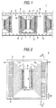
- Fig. 1 is a partly plan view showing an embodiment of a TAB tape carrier according to the invention.
- Fig. 2 is a partly enlarged plan view of the TAB tape carrier depicted in Fig. 1.
- Fig. 3 is a partly bottom view of the TAB tape carrier depicted in Fig. 1.
- the TAB tape carrier 1 includes a tape-shaped insulating layer 2 extending continuously in a lengthwise direction, a plurality of mount portions 3 for mounting electronic parts (not shown), a reinforcing layer 4 (see Fig. 3) for reinforcing the insulating layer 2, and a pair of carrier portions 5 for carrying the TAB tape carrier 1.
- the plurality of mount portions 3 are provided on the insulating layer 2 so as to be arranged continuously at a predetermined interval in a lengthwise direction of the insulating layer 2 (which is the same as the lengthwise direction of the TAB tape carrier 1 and may be referred simply to as lengthwise direction hereinafter). As shown in Fig. 2, each of the mount portions 3 is shaped like approximately a rectangle. An approximately rectangular mount area 6 formounting (placing) an electronic part (not shown) is provided in the center of each mount portion 3. Electric conductor patterns 7 are formed on opposite sides respectively in the lengthwise direction of each mount area 6.
- the electric conductor patterns 7 are formed on a front surface of the insulating layer 2.
- the electric conductor patterns 7 are made of a plurality of wires 8 arranged at a predetermined interval.
- Each of the wires 8 has an inner lead 9, an outer lead 10, and an intermediate lead 11 which are continuously integrated with one another.
- the respective inner leads 9 face the inside of the mount areas 6 and extend along the lengthwise direction.
- the inner leads 9 are disposed at a predetermined interval so as to be parallel with one another in a widthwise direction of the TAB tape carrier 1 (which is a direction perpendicular to the lengthwise direction and may be referred simply to as widthwise direction hereinafter) .
- the pitch i.e., the sum of the width of one inner lead 9 and the width (distance) between two adjacent inner leads 9) IP between the inner leads 9 is selected to be not larger than 60 ⁇ m, preferably not larger than 50 ⁇ m and generally not smaller than 10 ⁇ m.
- each inner lead 9 is selected to be in a range of from 5 ⁇ m to 50 ⁇ m, preferably in a range of from 10 ⁇ m to 40 ⁇ m.
- the width (distance) between two adjacent inner leads 9 is selected to be in a range of from 5 ⁇ m to 50 ⁇ m, preferably in a range of from 10 ⁇ m to 40 ⁇ m.
- the respective outer leads 10 face opposite end portions in the lengthwise direction of the mount portions 3 and extend along the lengthwise direction.
- the outer leads 10 are disposed at a predetermined interval so as to be parallel with one another in the widthwise direction.
- the pitch i.e., the sum of the width of one outer lead 10 and the width (distance) between two adjacent outer leads 10) OP between the outer leads 10 is selected to be in a range of from about 100 % to about 1000 % as large as the pitch IP between the inner leads 9. That is, the pitch OP between the outer leads 10 may be selected to be wider than the pitch IP between the inner leads 9 or to be substantially equal to the pitch IP between the inner leads 9.
- the intermediate leads 11 interlink the inner leads 9 with the outer leads 10 respectively so that the inner leads 9 are connected to the outer leads 10 respectively.
- the intermediate leads 11 are disposed so as to be spread radially in the lengthwise direction from the narrow-pitch inner lead 9 side to the wide-pitch outer lead 10 side.
- An insulating layer 12 of a solder resist or the like is provided in areas in which the intermediate leads 11 are disposed. That is, the insulating layer 12 of a solder resist or the like is shaped like approximately rectangular frames surrounding the mount areas 6 respectively and is provided so that all the intermediate leads 11 are covered with the insulating layer 12.
- the inner leads 9 and the outer leads 10 are preferably covered with a nickel-plating layer or a gold-plating layer suitably as will be described later.
- the reinforcing layer 4 is provided in all areas of a rear surface of the insulating layer 2 except positions which are opposite to the mount portions 3 so that positions where the mount portions 3 are formed on the insulating layer 2 are formed as opening portions 18.
- the reinforcing layer 4 is made of stainless steel foil and formed by carrier portion-reinforcing portions 13 and mount portion gap-reinforcing portions 14 continuously integrated with the carrier portion-reinforcing portions 13, the carrier portion-reinforcing portions 13 being provided continuously along the lengthwise direction at opposite side edge portions in the widthwise direction of the TAB tape carrier 1, the mount portion gap-reinforcing portions 14 being provided along the widthwise direction in gaps between the mountportions 3 arranged at a predetermined interval in the lengthwise direction.
- the formation of the carrier portion-reinforcing portions 13 permits improvement of strength at the time of carrying the TAB tape carrier 1.
- the formation of the mount portion gap-reinforcing portions 14 permits improvement of handling property at the time of mounting electronic parts or on other occasions.
- each carrier portion-reinforcing portion 13 is selected to be, for example, in a range of from 5 mm to 15 mm, preferably in a range of from 5 mm to 10 mm whereas the lengthwise length L2 of each mount portion gap-reinforcing port ion 14 is selected to be, for example, in a range of from 1 mm to 10 mm, preferably in a range of from 1 mm to 5 mm.
- the carrier portions 5 are provided along the lengthwise direction at opposite side edge portions in the widthwise direction of the TAB tape carrier 1.
- Two groups of feeding holes 15 are provided in the carrier portions 5 respectively so that the sprockets holes 15 can be engaged with sprockets or the like in order to carry the TAB tape carrier 1.
- the two groups of feeding holes 15 are formed so as to be opposite to each other in the widthwise direction.
- the feeding holes 15 are formed in the TAB tape carrier 1 so that each group of feeding holes 15 pierce the TAB tape carrier 1 (i.e., pierce the insulating layer 2 and the reinforcing layer 4) at a predetermined interval in the lengthwise direction of the TAB tape carrier 1 while each feeding hole 15 is shaped like approximately a rectangle.
- each feeding hole 15 is formed so as to be shaped like a square having a size of 1.981 mm X 1.981 mm.
- the distance between adjacent feeding holes 15 is selected, for example, to be 4.75 mm.
- TAB tape carrier 1 A method for producing the TAB tape carrier 1 will be described below with reference to Figs. 4 and 5.
- a reinforcing layer 4 is prepared as shown in Fig. 4A.
- Stainless steel foil is used as the reinforcing layer 4.
- any stainless steel can be used without any particular limitation.
- stainless steel having a thickness of from 3 ⁇ m to 100 ⁇ m, particularly from 5 ⁇ m to 30 ⁇ m, more particularly from 8 ⁇ m to 20 ⁇ m is used as the stainless steel foil.
- a long tape-shaped sheet of stainless steel foil having a width of from 100 mm to 1000 mm, preferably from about 150 mm to about 400 mm is prepared as the stainless steel foil.
- Figs. 4 and 5 show the form of a row of TAB tape carrier 1
- rows of TAB taper carriers 1 are generally slit one by one after the rows of TAB taper carriers 1 are produced simultaneously in the widthwise direction of the stainless steel foil.
- four rows of 48 mm-wide TAB tape carriers 1 can be produced simultaneously on 250 mm-wide stainless steel foil, or four rows of 70 mm-wide TAB tape carriers 1 can be produced simultaneously on 300 mm-wide stainless steel foil.
- an insulating layer 2 is formed on the reinforcing layer 4.
- a synthetic resin such as polyimide resin, acrylic resin, polyether-nitrile resin, polyether-sulfone resin, polyethylene terephthalate resin, polyethylene naphthalate resin, or polyvinyl chloride resin is used as an electrically insulating material for forming the insulating layer 2.
- polyimide resin is used as the electrically insulating material.
- the insulating layer 2 can be formed on the reinforcing layer 4 as follows. After a resin solution is applied on the reinforcing layer 4, the resin solution is dried and then heated to be cured. The aforementioned resin can be dissolved in an organic solvent or the like to thereby prepare the resin solution.
- a solution of polyamic acid resin which is a precursor of polyimide is used as the resin solution.
- a known coating method such as a doctor blade method, or a spin coating method can be used suitably for application of the resin.
- the resin solution is heated, for example, at a temperature of from 200°C to 600°C to be cured. In this manner, the insulating layer 2 made of a flexible resin film is formed on the reinforcing layer 4.
- the insulating layer 2 may be also formed in such a manner that a resin formed as a film in advance is stuck onto the reinforcing layer 4 through an adhesive agent.
- the insulating layer 2 may be also formed in such a manner that a solution of a photosensitive resin such as a photosensitive polyamic acid resin is applied on the reinforcing layer 4, exposed to light and developed to form predetermined patterns.
- a photosensitive resin such as a photosensitive polyamic acid resin
- the thickness of the insulating layer 2 formed thus is not larger than 50 ⁇ m, preferably not larger than 30 ⁇ m, more preferably not larger than 15 ⁇ m and generally not smaller than 3 ⁇ m.
- the thickness of the insulating layer 2 can be reduced as described above because flexible and high-strength stainless steel foil is used as the reinforcing layer 4.
- an electric conductor pattern 7 is formed as the wiring circuit pattern on a front surface of the insulating layer 2.
- copper, nickel, gold, solder or an alloy of these materials is used as an electric conductor for forming the electric conductor pattern 7.
- copper is used as the electric conductor.
- the formation of the electric conductor pattern 7 is not particularly limited.
- the electric conductor pattern 7 may be formed as the wiring circuit pattern on a front surface of the insulating layer 2 by a known patterning method such as a subtractive method, an additive method, or a semi-additive method.
- the subtractive method is carried out as follows. First, an electric conductor layer is laminated on the whole front surface of the insulating layer 2 through an adhesive layer if necessary. Then, an etching resist corresponding to the wiring circuit pattern is formed on the electric conductor layer . The electric conductor layer is etched with the etching resist used as a resist. Then, the etching resist is removed.
- the additive method is carried out as follows. First, a plating resist is formed as a pattern reverse to the wiring circuit pattern on the insulating layer 2. Then, an electric conductor pattern 7 is formed as the wiring circuit pattern by plating on a front surface of the insulating layer 2 except portions where the plating resist is formed. Then, the plating resist is removed.
- the semi-additivemethod is carried out as follows. First, a thin film of an electric conductor is formed as an undercoat on the insulating layer 2. Then, a plating resist is formed as a pattern reverse to the wiring circuit pattern on the undercoat. Then, an electric conductor pattern 7 is formed as the wiring circuit pattern by plating on a front surface of the undercoat except portions where the plating resist is formed. Then, the plating resist and the undercoat on which the plating resist is laminated are removed.
- the semi-additive method is preferably used as shown in Fig. 4C to Fig. 5D.
- a thin film of an electric conductor is formed as an undercoat 16 on the whole front surface of the insulating layer 2.
- a vacuum vapor deposition method especially a sputtering vapor deposition method is preferably used for the formation of the undercoat 16.
- Chromium, copper, etc. is preferably used as the electric conductor for forming the undercoat 16. More specifically, for example, a chromium thin film and a copper thin film are preferably formed successively on the whole front surface of the insulating layer 2 by a sputtering vapor deposition method.
- the undercoat 16 is preferably formed so that the thickness of the chromium thin film is selected to be in a range of from 100 ⁇ to 600 ⁇ whereas the thickness of the copper thin film is selected to be in a range of from 500 ⁇ to 2000 ⁇ .
- the plurality of feeding holes 15 are formed at opposite side edge portions in the widthwise direction of the TAB tape carrier 1 so as to be arranged along the lengthwise direction so that each feeding hole 15 pierces the reinforcing layer 4, the insulating layer 2 and the undercoat 16 in the direction of the thickness of the TAB tape carrier 1.
- a known processing method such as a drilling method, a laser machining method, a punching method, or an etching method can be used for the formation of the feeding holes 15.
- a punching method is used for the formation of the feeding holes 15.
- a plating resist 17 is formed as a pattern reverse to the wiring circuit pattern on the undercoat 16.
- the plating resist 17 can be formed as a predetermined resist pattern by a known method, for example, using a dry film resist.
- the plating resist 17 is also formed on the whole front surface of the reinforcing layer 4.
- an electric conductor pattern 7 is formed as the wiring circuit pattern by plating on a surface of the undercoat 16 except portions where the plating resist 17 is formed.
- Either electroplating or electroless plating maybe used as the plating.
- electroplating is used.
- copper electroplating is preferably used.
- the plating resist 17 is removed by a known etching method such as chemical etching (wet etching) or by peeling.
- the undercoat 16 on which the plating resist 17 was formed is removed by a known etching method such as chemical etching (wet etching) in the same manner as described above.
- the electric conductor pattern 7 is formed on the insulating layer 2 so that the electric conductor pattern 7 is provided as a wiring circuit pattern of wires 8 each having an inner lead 9, an outer lead 10 and an intermediate lead 11 continuously integrated with one another as described above.
- the thickness of the electric conductor pattern 7 formed thus is ina range of from 3 ⁇ m to 50 ⁇ m, preferably in a range of from 5 ⁇ m to 25 ⁇ m.
- a not-shown insulating layer 12 made of a solder resist or the like is formed to enclose the mount areas 6 so that the intermediate lead 11 of each wire 8 is covered with the insulating layer 12. Then, exposed portions of each wire 8, that is, the inner lead 9 and the outer lead 10 in each wire 8 are covered with a nickel plating layer and a gold plating layer.
- the insulating layer 12 can be formed as the aforementioned pattern by use of a photosensitive solder resist.
- the nickel plating layer and the gold plating layer can be formed by nickel plating and gold plating respectively.
- opening portions 18 are formed in the reinforcing layer 4 in positions where the reinforcing layer 4 overlaps the mount portions 3.
- the TAB tape carrier 1 is obtained.
- portions of the reinforcing layer 4 corresponding to the slit portions between adjacent rows of the TAB tape carriers 1 are preferably removed in the same manner as the opening portions 18.
- the opening portions 18 can be formed in the reinforcing layer 4 in such a manner that portions of the reinforcing layer 4 opposite to the mount portions 3 are opened by a known method such as drilling, punching, or wet etching (chemical etching) .
- a known method such as drilling, punching, or wet etching (chemical etching) .
- formation of the opening portions 18 in the reinforcing layer 4 by etching can be carried out as follows. Portions of the reinforcing layer 4 except the opening portions 18 are covered with an etching resist. Then, the reinforcing layer 4 is etched with a known etching solution such as a ferric chloride solution. Then, the etching resist is removed. After the etching, the rows of TAB tape carriers 1 are slit one by one if the rows of TAB tape carriers 1 are produced simultaneously in the widthwise direction of the reinforcing layer 4.
- the reinforcing layer 4 of stainless steel foil more flexible and having a higher strength than copper foil is formed on a rear surface of the insulating layer 2 in the TAB tape carrier 1 obtained thus, the strength of the TAB tape carrier 1 can be enhanced sufficiently at the time of carrying the TAB tape carrier or at the time of mounting and bonding electronic parts while the insulating layer 2 can be formed thinly. Accordingly,both dimensionalaccuracy and positional accuracy can be improved at the time of carrying the TAB tape carrier or at the time of mounting and bonding electronic parts. While reduction in weight, thickness and size can be attained, electronic parts can be mounted surely in such high-density wiring that the pitch between the inner leads 9 in the electric conductor pattern 7 is not larger than 60 ⁇ m.
- the reinforcing layer 4 is provided on the whole area of the rear surface of the insulating layer 2 except positions opposite to the mount portions 3, the positions where the reinforcing layer 4 is provided are not particularly limited and can be selected suitably according to the purpose and usage.
- the reinforcing layer 4 maybe provided in positions opposite to the mount portions 3 so that heat-radiating characteristic can be improved.
- Stainless steel foil (SUS304, 250 mm wide) 20 ⁇ m thick was prepared as a reinforcing layer (see Fig. 4A) .
- a solution of a polyamic acid resin was applied on the reinforcing layer, dried and heated to be cured to thereby form an insulating layer of apolyimide resin 12 ⁇ m thick (see Fig. 4B) .
- a chromium thin film and a copper thin film were formed successively on a front surface of the insulating layer by a sputtering vapor deposition method to thereby form an undercoat 2000 ⁇ thick (see Fig. 4C).
- Figs. 4A and 5E show the form of one row of TAB tape carrier
- Example 1 shows the case where four rows of 48 mm-wide TAB tape carriers are produced simultaneously on 250 mm-wide stainless steel foil.
- feeding holes were formed by punching so that each feeding hole pierced the reinforcing layer, the insulating layer and the undercoat in the direction of the thickness of the TAB tape carrier (see Fig. 4D) .
- a plating resist was formed as a predetermined pattern on a surface of the undercoat and formed on the whole front surface of the reinforcing layer (see Fig. 5A).
- the resulting sheet was immersed in an electrolytic copper sulfate plating solution so thatportions of the undercoat except portions where the plating resist was formed were electroplated with copper at the rate of 2.5 A/dm 2 for about 20 minutes to thereby form an electric conductor pattern 10 ⁇ m thick (see Fig. 5B).
- the electric conductor pattern was formed as a plurality of wiring patterns arranged at a predetermined interval and each having an inner lead, an outer lead and an intermediate lead continuously integrated with one another.
- the pitch between the inner leads was 30 ⁇ m whereas the pitch between the outer leads was 100 ⁇ m.
- the plating resist was removed by chemical etching (see Fig. 5C). Then, the undercoat on which the plating resist had been formed was removed by chemical etching in the same manner as described above (see Step Fig. 5D).
- aphotosensitive solder resist was formed to enclose the mount areas so that the intermediate lead of each wire was covered with the photosensitive solder resist. Then, the inner leads and the outer leads were covered by nickel plating and gold plating.
- portions of the reinforcing layer except positions overlapping the mount portions were covered with an etching resist.
- the reinforcing layer was etched with a ferric chloride solution to thereby form opening portions and slit portions between TAB tape carriers.
- the etching resist was removed and slit to thereby obtain TAB tape carriers.
- TAB taper carriers were obtained in the same manner as in Example 1 except that copper foil 20 ⁇ m thick was used as the reinforcing layer.
- the distance between two inner leads located at opposite ends in the widthwise direction i.e., the distance between the widthwise centers of inner leads located at opposite ends as represented by the sign "X" in Fig. 2 was measured and compared with a design size. Results of the measurement were as follows. Incidentally, the measured value was an average of values measured 20 times.
- the reinforcing layer of stainless steel foil which is more flexible and has a higher strength than copper foil is formed on a rear surface of the insulating layer. Accordingly, while the insulating layer can be formed thinly, both dimensional accuracy and positional accuracy can be improved at the time of carrying the TAB tape carrier or at the time of mounting and bonding electronic parts. Accordingly, while reduction in weight, thickness and size can be attained, electronic parts can be mounted surely in such high-density wiring that the pitch between wires in the electric conductor pattern is not larger than 60 ⁇ m.
Landscapes
- Engineering & Computer Science (AREA)
- Manufacturing & Machinery (AREA)
- Microelectronics & Electronic Packaging (AREA)
- Wire Bonding (AREA)
Abstract
Description
- The present invention relates to a tape carrier for TAB (hereinafter referred to as TAB tape carrier) and particularly to a TAB tape carrier for mounting electronic parts by a TAB method.
- A TAB tape carrier is widely used for mounting electronic parts such as semiconductor devices by a TAB (Tape Automated Bonding) method.
- A demand for reduction in weight, thickness and size of such a TAB tape carrier has been increasing with the advance of the demand for reduction in weight, thickness and size of electronic parts in recent years.
- On the other hand, such a TAB tape carrier is generally carried in the condition that sprockets are engaged with feeding holes formed along a lengthwise direction of the TAB tape carrier at opposite end portions in a widthwise direction of the TAB tape carrier so that a predetermined amount of tension is applied to the TAB tape carrier. For this reason, if the TAB tape carrier is formed so as to be too thin, the feeding holes may be broken at the time of carrying the TAB tape carrier or the positions of the feeding holes may be displaced at the time of mounting and bonding electronic parts.
- Therefore, forexample, JP-A-5-29394, JP-A-2000-332062, and JP-A-2000-340617 have proposed the provision of a sheet of copper foil on a rear surface of an electrically insulating film to reinforce the electrically insulating film in the condition that electric conductor patterns are formed on.a front surface of the electrically insulating film.
- The demand for reduction in weight, thickness and size and the demand for reduction in size and density of the electric conductor patterns have been increasing in recent years. These demands cannot be satisfied sufficiently by the reinforcing effect of copper foil. To satisfy these demands, greater improvement in dimensional accuracy and positional accuracy has been required at the time of carrying the TAB tape carrier or at the time of mounting and bonding electronic parts.
- The invention is developed upon such circumstances and an object of the invention is to provide a TAB tape carrier in which high-density wiring can be achieved while reduction in weight, thickness and size is attained as well as improvement in dimensional accuracy and positional accuracy in the TAB tape carrier can be achieved at the time of carrying the TAB tape carrier or at the time of mounting and bonding electronic parts.
- In order to achieve the obj ect, according to the invention, there is provided a tape carrier for TAB including: an insulating layer; electric conductor patterns formed on a front surface of the insulating layer and each made of a plurality of wires arranged at a predetermined interval; and a reinforcing layer of stainless steel foil formed on a rear surface of the insulating layer so as to be provided along a lengthwise direction of the insulating layer at opposite side edge portions in a widthwise direction of the insulating layer. The wires may be arranged at a predetermined interval of a pitch of not larger than 60 µm.
- In the tape carrier for TAB according to the invention, the insulating layer can be formed to have a thickness of not larger than 50 µm.
-
- Fig. 1 is a partly plan view showing an embodiment of a TAB tape carrier according to the invention;
- Fig. 2 is a partly enlarged plan view of the TAB tape carrier depicted in Fig. 1;
- Fig. 3 is a partly bottom view of the TAB tape carrier depicted in Fig. 1;
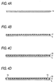
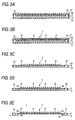
- Figs. 4A through 4D, and 5A through 5E show steps of a method for producing the TAB tape carrier according to the invention in a section taken along the line A-A' in Fig. 2:
- Fig. 4A is the step of preparing a reinforcing layer;
- Fig. 4B is the step of forming an insulating layer on the reinforcing layer;
- Fig. 4C is the step of forming an undercoat on the whole front surface of the insulating layer;
- Fig. 4D is the step of forming feeding holes;
- Fig. 5A is the step of forming a plating resist on the undercoat;
- Fig. 5B is the step of forming an electric conductor pattern by plating on portions of the undercoat layer except portions where the plating resist is formed;
- Fig. 5C is the step of removing the plating resist;
- Fig. 5D is the step of removing the undercoat on which the plating resist was formed; and
- Fig. 5E is the step of forming opening portions in the reinforcing layer in positions where the reinforcing layer overlaps the mount portions.
-
- Fig. 1 is a partly plan view showing an embodiment of a TAB tape carrier according to the invention. Fig. 2 is a partly enlarged plan view of the TAB tape carrier depicted in Fig. 1. Fig. 3 is a partly bottom view of the TAB tape carrier depicted in Fig. 1.
- In Fig. 1, the
TAB tape carrier 1 includes a tape-shaped insulating layer 2 extending continuously in a lengthwise direction, a plurality ofmount portions 3 for mounting electronic parts (not shown), a reinforcing layer 4 (see Fig. 3) for reinforcing theinsulating layer 2, and a pair ofcarrier portions 5 for carrying theTAB tape carrier 1. - The plurality of
mount portions 3 are provided on theinsulating layer 2 so as to be arranged continuously at a predetermined interval in a lengthwise direction of the insulating layer 2 (which is the same as the lengthwise direction of theTAB tape carrier 1 and may be referred simply to as lengthwise direction hereinafter). As shown in Fig. 2, each of themount portions 3 is shaped like approximately a rectangle. An approximatelyrectangular mount area 6 formounting (placing) an electronic part (not shown) is provided in the center of eachmount portion 3.Electric conductor patterns 7 are formed on opposite sides respectively in the lengthwise direction of eachmount area 6. - The
electric conductor patterns 7 are formed on a front surface of theinsulating layer 2. Theelectric conductor patterns 7 are made of a plurality ofwires 8 arranged at a predetermined interval. Each of thewires 8 has aninner lead 9, anouter lead 10, and anintermediate lead 11 which are continuously integrated with one another. - The respective
inner leads 9 face the inside of themount areas 6 and extend along the lengthwise direction. Theinner leads 9 are disposed at a predetermined interval so as to be parallel with one another in a widthwise direction of the TAB tape carrier 1 (which is a direction perpendicular to the lengthwise direction and may be referred simply to as widthwise direction hereinafter) . The pitch (i.e., the sum of the width of oneinner lead 9 and the width (distance) between two adjacent inner leads 9) IP between theinner leads 9 is selected to be not larger than 60 µm, preferably not larger than 50 µm and generally not smaller than 10 µm. When the pitch IP between theinner leads 9 is selected to be not larger than 60 µm in thismanner,high-density wiring can beprovided. Incidentally, in theTAB tape carrier 1, such high-density wiring can be achieved because flexible and high-strength stainless steel foil is used as the reinforcinglayer 4 as will be described later. - The width of each
inner lead 9 is selected to be in a range of from 5 µm to 50 µm, preferably in a range of from 10 µm to 40 µm. The width (distance) between two adjacentinner leads 9 is selected to be in a range of from 5 µm to 50 µm, preferably in a range of from 10 µm to 40 µm. - The respective outer leads 10 face opposite end portions in the lengthwise direction of the
mount portions 3 and extend along the lengthwise direction. Theouter leads 10 are disposed at a predetermined interval so as to be parallel with one another in the widthwise direction. For example, the pitch (i.e., the sum of the width of oneouter lead 10 and the width (distance) between two adjacent outer leads 10) OP between theouter leads 10 is selected to be in a range of from about 100 % to about 1000 % as large as the pitch IP between theinner leads 9. That is, the pitch OP between theouter leads 10 may be selected to be wider than the pitch IP between theinner leads 9 or to be substantially equal to the pitch IP between theinner leads 9. - The intermediate leads 11 interlink the inner leads 9 with the outer leads 10 respectively so that the inner leads 9 are connected to the outer leads 10 respectively. The intermediate leads 11 are disposed so as to be spread radially in the lengthwise direction from the narrow-pitch
inner lead 9 side to the wide-pitchouter lead 10 side. - An insulating
layer 12 of a solder resist or the like is provided in areas in which the intermediate leads 11 are disposed. That is, the insulatinglayer 12 of a solder resist or the like is shaped like approximately rectangular frames surrounding themount areas 6 respectively and is provided so that all the intermediate leads 11 are covered with the insulatinglayer 12. - Incidentally, the inner leads 9 and the outer leads 10 are preferably covered with a nickel-plating layer or a gold-plating layer suitably as will be described later.
- As shown in Fig. 3, the reinforcing
layer 4 is provided in all areas of a rear surface of the insulatinglayer 2 except positions which are opposite to themount portions 3 so that positions where themount portions 3 are formed on the insulatinglayer 2 are formed as openingportions 18. More specifically, the reinforcinglayer 4 is made of stainless steel foil and formed by carrier portion-reinforcingportions 13 and mount portion gap-reinforcingportions 14 continuously integrated with the carrier portion-reinforcingportions 13, the carrier portion-reinforcingportions 13 being provided continuously along the lengthwise direction at opposite side edge portions in the widthwise direction of theTAB tape carrier 1, the mount portion gap-reinforcingportions 14 being provided along the widthwise direction in gaps between themountportions 3 arranged at a predetermined interval in the lengthwise direction. The formation of the carrier portion-reinforcingportions 13 permits improvement of strength at the time of carrying theTAB tape carrier 1. The formation of the mount portion gap-reinforcingportions 14 permits improvement of handling property at the time of mounting electronic parts or on other occasions. - Incidentally, the widthwise length L1 of each carrier portion-reinforcing
portion 13 is selected to be, for example, in a range of from 5 mm to 15 mm, preferably in a range of from 5 mm to 10 mm whereas the lengthwise length L2 of each mount portion gap-reinforcingport ion 14 is selected to be, for example, in a range of from 1 mm to 10 mm, preferably in a range of from 1 mm to 5 mm. - As shown in Fig. 1, the
carrier portions 5 are provided along the lengthwise direction at opposite side edge portions in the widthwise direction of theTAB tape carrier 1. Two groups of feedingholes 15 are provided in thecarrier portions 5 respectively so that the sprockets holes 15 can be engaged with sprockets or the like in order to carry theTAB tape carrier 1. The two groups of feedingholes 15 are formed so as to be opposite to each other in the widthwise direction. The feeding holes 15 are formed in theTAB tape carrier 1 so that each group of feedingholes 15 pierce the TAB tape carrier 1 (i.e., pierce the insulatinglayer 2 and the reinforcing layer 4) at a predetermined interval in the lengthwise direction of theTAB tape carrier 1 while each feedinghole 15 is shaped like approximately a rectangle. - Incidentally, for example, each feeding
hole 15 is formed so as to be shaped like a square having a size of 1.981 mm X 1.981 mm. The distance between adjacent feeding holes 15 is selected, for example, to be 4.75 mm. - A method for producing the
TAB tape carrier 1 will be described below with reference to Figs. 4 and 5. - In the method, first, a reinforcing
layer 4 is prepared as shown in Fig. 4A. Stainless steel foil is used as the reinforcinglayer 4. Incidentally, there are various kinds of stainless steel such as SUS301, SUS304, SUS305, SUS309, SUS310, SUS316, SUS317, SUS321, and SUS347 according to the AISI (American Iron and Steel Institute) standard. Any stainless steel can be used without any particular limitation. Preferably, stainless steel having a thickness of from 3 µm to 100 µm, particularly from 5 µm to 30 µm, more particularly from 8 µm to 20 µm is used as the stainless steel foil. In practice, a long tape-shaped sheet of stainless steel foil having a width of from 100 mm to 1000 mm, preferably from about 150 mm to about 400 mm is prepared as the stainless steel foil. - Although Figs. 4 and 5 show the form of a row of
TAB tape carrier 1, rows ofTAB taper carriers 1 are generally slit one by one after the rows ofTAB taper carriers 1 are produced simultaneously in the widthwise direction of the stainless steel foil. - For example, four rows of 48 mm-wide
TAB tape carriers 1 can be produced simultaneously on 250 mm-wide stainless steel foil, or four rows of 70 mm-wideTAB tape carriers 1 can be produced simultaneously on 300 mm-wide stainless steel foil. - Then, as shown in Fig. 4B an insulating
layer 2 is formed on the reinforcinglayer 4. For example, a synthetic resin such as polyimide resin, acrylic resin, polyether-nitrile resin, polyether-sulfone resin, polyethylene terephthalate resin, polyethylene naphthalate resin, or polyvinyl chloride resin is used as an electrically insulating material for forming the insulatinglayer 2. Preferably, polyimide resin is used as the electrically insulating material. - For example, the insulating
layer 2 can be formed on the reinforcinglayer 4 as follows. After a resin solution is applied on the reinforcinglayer 4, the resin solution is dried and then heated to be cured. The aforementioned resin can be dissolved in an organic solvent or the like to thereby prepare the resin solution. For example, a solution of polyamic acid resin which is a precursor of polyimide is used as the resin solution. A known coating method such as a doctor blade method, or a spin coating method can be used suitably for application of the resin. After heated suitably to be dried, the resin solution is heated, for example, at a temperature of from 200°C to 600°C to be cured. In this manner, the insulatinglayer 2 made of a flexible resin film is formed on the reinforcinglayer 4. - The insulating
layer 2 may be also formed in such a manner that a resin formed as a film in advance is stuck onto the reinforcinglayer 4 through an adhesive agent. - The insulating
layer 2 may be also formed in such a manner that a solution of a photosensitive resin such as a photosensitive polyamic acid resin is applied on the reinforcinglayer 4, exposed to light and developed to form predetermined patterns. - For example, the thickness of the insulating
layer 2 formed thus is not larger than 50 µm, preferably not larger than 30 µm, more preferably not larger than 15 µm and generally not smaller than 3 µm. Incidentally, in theTAB tape carrier 1, the thickness of the insulatinglayer 2 can be reduced as described above because flexible and high-strength stainless steel foil is used as the reinforcinglayer 4. - Then, in the method, an
electric conductor pattern 7 is formed as the wiring circuit pattern on a front surface of the insulatinglayer 2. For example, copper, nickel, gold, solder or an alloy of these materials is used as an electric conductor for forming theelectric conductor pattern 7. Preferably, copper is used as the electric conductor. The formation of theelectric conductor pattern 7 is not particularly limited. Theelectric conductor pattern 7 may be formed as the wiring circuit pattern on a front surface of the insulatinglayer 2 by a known patterning method such as a subtractive method, an additive method, or a semi-additive method. - The subtractive method is carried out as follows. First, an electric conductor layer is laminated on the whole front surface of the insulating
layer 2 through an adhesive layer if necessary. Then, an etching resist corresponding to the wiring circuit pattern is formed on the electric conductor layer . The electric conductor layer is etched with the etching resist used as a resist. Then, the etching resist is removed. - The additive method is carried out as follows. First, a plating resist is formed as a pattern reverse to the wiring circuit pattern on the insulating
layer 2. Then, anelectric conductor pattern 7 is formed as the wiring circuit pattern by plating on a front surface of the insulatinglayer 2 except portions where the plating resist is formed. Then, the plating resist is removed. - The semi-additivemethod is carried out as follows. First, a thin film of an electric conductor is formed as an undercoat on the insulating
layer 2. Then, a plating resist is formed as a pattern reverse to the wiring circuit pattern on the undercoat. Then, anelectric conductor pattern 7 is formed as the wiring circuit pattern by plating on a front surface of the undercoat except portions where the plating resist is formed. Then, the plating resist and the undercoat on which the plating resist is laminated are removed. - Of these patterning methods, the semi-additive method is preferably used as shown in Fig. 4C to Fig. 5D.
- That is, in the semi-additive method, first, as shown in Fig. 4C, a thin film of an electric conductor is formed as an
undercoat 16 on the whole front surface of the insulatinglayer 2. A vacuum vapor deposition method, especially a sputtering vapor deposition method is preferably used for the formation of theundercoat 16. Chromium, copper, etc. is preferably used as the electric conductor for forming theundercoat 16. More specifically, for example, a chromium thin film and a copper thin film are preferably formed successively on the whole front surface of the insulatinglayer 2 by a sputtering vapor deposition method. Incidentally, for example, theundercoat 16 is preferably formed so that the thickness of the chromium thin film is selected to be in a range of from 100Å to 600Å whereas the thickness of the copper thin film is selected to be in a range of from 500Å to 2000Å. - Then, in this method, as shown in Fig. 4D, the plurality of feeding
holes 15 are formed at opposite side edge portions in the widthwise direction of theTAB tape carrier 1 so as to be arranged along the lengthwise direction so that each feedinghole 15 pierces the reinforcinglayer 4, the insulatinglayer 2 and theundercoat 16 in the direction of the thickness of theTAB tape carrier 1. A known processing method such as a drilling method, a laser machining method, a punching method, or an etching method can be used for the formation of the feeding holes 15. Preferably, a punching method is used for the formation of the feeding holes 15. - Then, in this method, as shown in Fig. 5A, a plating resist 17 is formed as a pattern reverse to the wiring circuit pattern on the
undercoat 16. The plating resist 17 can be formed as a predetermined resist pattern by a known method, for example, using a dry film resist. Incidentally, the plating resist 17 is also formed on the whole front surface of the reinforcinglayer 4. - Then, as shown in Fig. 5B, an
electric conductor pattern 7 is formed as the wiring circuit pattern by plating on a surface of theundercoat 16 except portions where the plating resist 17 is formed. Either electroplating or electroless plating maybe used as the plating. Preferably, electroplating is used. Especially, copper electroplating is preferably used. - Then, as shown in Fig. 5C, the plating resist 17 is removed by a known etching method such as chemical etching (wet etching) or by peeling. Then, as shown in Fig. 5D, the
undercoat 16 on which the plating resist 17 was formed is removed by a known etching method such as chemical etching (wet etching) in the same manner as described above. As a result, theelectric conductor pattern 7 is formed on the insulatinglayer 2 so that theelectric conductor pattern 7 is provided as a wiring circuit pattern ofwires 8 each having aninner lead 9, anouter lead 10 and anintermediate lead 11 continuously integrated with one another as described above. - For example, the thickness of the
electric conductor pattern 7 formed thus is ina range of from 3 µm to 50 µm, preferably in a range of from 5 µm to 25 µm. - Then, a not-shown insulating
layer 12 made of a solder resist or the like is formed to enclose themount areas 6 so that theintermediate lead 11 of eachwire 8 is covered with the insulatinglayer 12. Then, exposed portions of eachwire 8, that is, theinner lead 9 and theouter lead 10 in eachwire 8 are covered with a nickel plating layer and a gold plating layer. For example, the insulatinglayer 12 can be formed as the aforementioned pattern by use of a photosensitive solder resist. The nickel plating layer and the gold plating layer can be formed by nickel plating and gold plating respectively. - Then, as shown in Fig. 5E, opening
portions 18 are formed in the reinforcinglayer 4 in positions where the reinforcinglayer 4 overlaps themount portions 3. Thus, theTAB tape carrier 1 is obtained. - Incidentally, when rows of
TAB tape carriers 1 are produced simultaneously in the widthwise direction of the reinforcinglayer 4 and then slit one by one, portions of the reinforcinglayer 4 corresponding to the slit portions between adjacent rows of theTAB tape carriers 1 are preferably removed in the same manner as the openingportions 18. - The opening
portions 18 can be formed in the reinforcinglayer 4 in such a manner that portions of the reinforcinglayer 4 opposite to themount portions 3 are opened by a known method such as drilling, punching, or wet etching (chemical etching) . For example, formation of the openingportions 18 in the reinforcinglayer 4 by etching can be carried out as follows. Portions of the reinforcinglayer 4 except the openingportions 18 are covered with an etching resist. Then, the reinforcinglayer 4 is etched with a known etching solution such as a ferric chloride solution. Then, the etching resist is removed. After the etching, the rows ofTAB tape carriers 1 are slit one by one if the rows ofTAB tape carriers 1 are produced simultaneously in the widthwise direction of the reinforcinglayer 4. - Since the reinforcing
layer 4 of stainless steel foil more flexible and having a higher strength than copper foil is formed on a rear surface of the insulatinglayer 2 in theTAB tape carrier 1 obtained thus, the strength of theTAB tape carrier 1 can be enhanced sufficiently at the time of carrying the TAB tape carrier or at the time of mounting and bonding electronic parts while the insulatinglayer 2 can be formed thinly. Accordingly,both dimensionalaccuracy and positional accuracy can be improved at the time of carrying the TAB tape carrier or at the time of mounting and bonding electronic parts. While reduction in weight, thickness and size can be attained, electronic parts can be mounted surely in such high-density wiring that the pitch between theinner leads 9 in theelectric conductor pattern 7 is not larger than 60 µm. - Although the above description has been made upon the case where the reinforcing
layer 4 is provided on the whole area of the rear surface of the insulatinglayer 2 except positions opposite to themount portions 3, the positions where the reinforcinglayer 4 is provided are not particularly limited and can be selected suitably according to the purpose and usage. For example, the reinforcinglayer 4 maybe provided in positions opposite to themount portions 3 so that heat-radiating characteristic can be improved. - The invention will be described below more specifically on the basis of the following example and comparative example.
- Stainless steel foil (SUS304, 250 mm wide) 20 µm thick was prepared as a reinforcing layer (see Fig. 4A) . A solution of a polyamic acid resin was applied on the reinforcing layer, dried and heated to be cured to thereby form an insulating layer of
apolyimide resin 12 µm thick (see Fig. 4B) . Then, a chromium thin film and a copper thin film were formed successively on a front surface of the insulating layer by a sputtering vapor deposition method to thereby form an undercoat 2000Å thick (see Fig. 4C). - Although Figs. 4A and 5E show the form of one row of TAB tape carrier, Example 1 shows the case where four rows of 48 mm-wide TAB tape carriers are produced simultaneously on 250 mm-wide stainless steel foil.
- Then, feeding holes were formed by punching so that each feeding hole pierced the reinforcing layer, the insulating layer and the undercoat in the direction of the thickness of the TAB tape carrier (see Fig. 4D) . Then, a plating resist was formed as a predetermined pattern on a surface of the undercoat and formed on the whole front surface of the reinforcing layer (see Fig. 5A).
- Then, the resulting sheet was immersed in an electrolytic copper sulfate plating solution so thatportions of the undercoat except portions where the plating resist was formed were electroplated with copper at the rate of 2.5 A/dm2 for about 20 minutes to thereby form an
electric conductor pattern 10 µm thick (see Fig. 5B). - Incidentally, the electric conductor pattern was formed as a plurality of wiring patterns arranged at a predetermined interval and each having an inner lead, an outer lead and an intermediate lead continuously integrated with one another. The pitch between the inner leads was 30 µm whereas the pitch between the outer leads was 100 µm.
- Then, the plating resist was removed by chemical etching (see Fig. 5C). Then, the undercoat on which the plating resist had been formed was removed by chemical etching in the same manner as described above (see Step Fig. 5D).
- Then, aphotosensitive solder resist was formed to enclose the mount areas so that the intermediate lead of each wire was covered with the photosensitive solder resist. Then, the inner leads and the outer leads were covered by nickel plating and gold plating.
- Then, portions of the reinforcing layer except positions overlapping the mount portions were covered with an etching resist. Then, the reinforcing layer was etched with a ferric chloride solution to thereby form opening portions and slit portions between TAB tape carriers. Then, the etching resist was removed and slit to thereby obtain TAB tape carriers.
- TAB taper carriers were obtained in the same manner as in Example 1 except that copper foil 20 µm thick was used as the reinforcing layer.
- In each of the TAB tape carriers obtained in Example 1 and Comparative Example 1, the distance between two inner leads located at opposite ends in the widthwise direction (i.e., the distance between the widthwise centers of inner leads located at opposite ends as represented by the sign "X" in Fig. 2) was measured and compared with a design size. Results of the measurement were as follows. Incidentally, the measured value was an average of values measured 20 times.
- Design Size: 21000 µm
- Example 1: 21002 µm, dimensional difference of 2 µm
- Comparative Example 1: 21020 µm, dimensional difference of 20 µm
-
- As described above, in the TAB tape carrier according to the invention, the reinforcing layer of stainless steel foil which is more flexible and has a higher strength than copper foil is formed on a rear surface of the insulating layer. Accordingly, while the insulating layer can be formed thinly, both dimensional accuracy and positional accuracy can be improved at the time of carrying the TAB tape carrier or at the time of mounting and bonding electronic parts. Accordingly, while reduction in weight, thickness and size can be attained, electronic parts can be mounted surely in such high-density wiring that the pitch between wires in the electric conductor pattern is not larger than 60 µm.
- The present application is based on Japanese Patent Application No. 2002-294787, the entire contents of which are incorporated herein by reference.
Claims (4)
- A tape carrier comprising:an insulating layer;electric conductor patterns formed on a front surface of said insulating layer and each made of a plurality of wires arranged at a predetermined interval; anda reinforcing layer of stainless steel foil formed on a rear surface of said insulating layer so as to be provided along a lengthwise direction of said insulating layer at opposite side edge portions in a widthwise direction of said insulating layer.
- A tape carrier according to Claim 1, wherein said wires are arranged with a pitch of not larger than 60 µm.
- A tape carrier according to Claim 1, wherein said insulating layer has a thickness of not larger than 50 µm.
- A tape carrier according to Claim 1, wherein feeding holes formed along a lengthwise direction of the tape carrier at opposite end portions in a widthwise direction of the tape carrier.
Applications Claiming Priority (2)
| Application Number | Priority Date | Filing Date | Title |
|---|---|---|---|
| JP2002294787A JP3694286B2 (en) | 2002-10-08 | 2002-10-08 | TAB tape carrier |
| JP2002294787 | 2002-10-08 |
Publications (2)
| Publication Number | Publication Date |
|---|---|
| EP1416535A2 true EP1416535A2 (en) | 2004-05-06 |
| EP1416535A3 EP1416535A3 (en) | 2008-04-23 |
Family
ID=32089190
Family Applications (1)
| Application Number | Title | Priority Date | Filing Date |
|---|---|---|---|
| EP03022844A Withdrawn EP1416535A3 (en) | 2002-10-08 | 2003-10-08 | Tape carrier for tab |
Country Status (6)
| Country | Link |
|---|---|
| US (1) | US7205482B2 (en) |
| EP (1) | EP1416535A3 (en) |
| JP (1) | JP3694286B2 (en) |
| KR (1) | KR100649842B1 (en) |
| CN (1) | CN1302531C (en) |
| TW (1) | TWI292194B (en) |
Cited By (1)
| Publication number | Priority date | Publication date | Assignee | Title |
|---|---|---|---|---|
| EP1786247A3 (en) * | 2005-11-14 | 2008-11-19 | Nitto Denko Corporation | Wired circuit board and method for manufacturing wired circuit board and mounting electronic component thereon |
Families Citing this family (12)
| Publication number | Priority date | Publication date | Assignee | Title |
|---|---|---|---|---|
| JP4628154B2 (en) * | 2005-03-22 | 2011-02-09 | 三井金属鉱業株式会社 | Flexible printed circuit board and semiconductor device |
| JP4619214B2 (en) | 2005-07-04 | 2011-01-26 | 日東電工株式会社 | Printed circuit board |
| JP2007035869A (en) * | 2005-07-26 | 2007-02-08 | Nitto Denko Corp | Tape carrier for TAB |
| KR100634238B1 (en) * | 2005-08-12 | 2006-10-16 | 삼성전자주식회사 | Tab Tape for Tape Carrier Packages |
| KR20070022472A (en) * | 2005-08-22 | 2007-02-27 | 삼성전자주식회사 | Tape wiring board for tape package with reinforcement layer |
| JP2007067272A (en) | 2005-09-01 | 2007-03-15 | Nitto Denko Corp | TAB tape carrier and method for manufacturing the same |
| JP3117072U (en) * | 2005-09-26 | 2006-01-05 | 船井電機株式会社 | Flexible flat cable and its assembly equipment |
| JP2008205172A (en) * | 2007-02-20 | 2008-09-04 | Shindo Denshi Kogyo Kk | Cof carrier tape, method of manufacturing cof carrier tape, and method of manufacturing cof semiconductor device |
| JP4306795B2 (en) * | 2007-05-18 | 2009-08-05 | 凸版印刷株式会社 | WIRING BOARD, SEMICONDUCTOR PACKAGE, ELECTRONIC DEVICE, AND WIRING BOARD MANUFACTURING METHOD |
| US8232655B2 (en) | 2008-01-03 | 2012-07-31 | International Business Machines Corporation | Bump pad metallurgy employing an electrolytic Cu / electorlytic Ni / electrolytic Cu stack |
| CN104821307B (en) * | 2015-04-27 | 2017-12-19 | 上海伊诺尔信息技术有限公司 | Belt for smart card and method for packing |
| US20200367358A1 (en) * | 2019-05-13 | 2020-11-19 | Honeywell Federal Manufacturing & Technologies, Llc | Conductive trace interconnection tape |
Citations (3)
| Publication number | Priority date | Publication date | Assignee | Title |
|---|---|---|---|---|
| JPH0582591A (en) * | 1991-09-19 | 1993-04-02 | Hitachi Cable Ltd | Semiconductor device film carrier |
| JPH10144735A (en) * | 1996-11-06 | 1998-05-29 | Sumitomo Metal Mining Co Ltd | Tape carrier with reinforcing plate and method of manufacturing the same |
| EP1599076A1 (en) * | 2004-05-20 | 2005-11-23 | Nitto Denko Corporation | Wired circuit board |
Family Cites Families (17)
| Publication number | Priority date | Publication date | Assignee | Title |
|---|---|---|---|---|
| US5001888A (en) * | 1990-01-16 | 1991-03-26 | Seagate Technology, Inc. | Method of packaging and dispensing a mechanical part |
| JPH0448629U (en) * | 1990-08-31 | 1992-04-24 | ||
| JP2705297B2 (en) * | 1990-10-09 | 1998-01-28 | 日立電線株式会社 | High strength TAB tape carrier |
| EP0529097B1 (en) * | 1991-03-12 | 2003-01-15 | Sumitomo Bakelite Company Limited | Method of manufacturing two-layer tab tape |
| JPH0529394A (en) | 1991-07-19 | 1993-02-05 | Hitachi Cable Ltd | TAB tape carrier |
| US5345039A (en) * | 1992-08-06 | 1994-09-06 | Minnesota Mining And Manufacturing Company | Film carrier |
| JPH0964108A (en) * | 1995-08-29 | 1997-03-07 | Hitachi Cable Ltd | TAB tape carrier |
| JPH09263082A (en) * | 1996-03-29 | 1997-10-07 | Toshiba Corp | IC module manufacturing method, IC card manufacturing method, and IC module |
| JP3520186B2 (en) * | 1996-09-30 | 2004-04-19 | 東芝マイクロエレクトロニクス株式会社 | Method for manufacturing film carrier tape, apparatus for manufacturing film carrier tape |
| JP3042613B2 (en) * | 1997-11-27 | 2000-05-15 | 日本電気株式会社 | Semiconductor device and manufacturing method thereof |
| JPH11238831A (en) * | 1997-12-16 | 1999-08-31 | Shinko Electric Ind Co Ltd | Tape carrier and manufacturing method thereof |
| JP3512655B2 (en) * | 1998-12-01 | 2004-03-31 | シャープ株式会社 | Semiconductor device, method of manufacturing the same, and reinforcing tape used for manufacturing the semiconductor device |
| US6320135B1 (en) * | 1999-02-03 | 2001-11-20 | Casio Computer Co., Ltd. | Flexible wiring substrate and its manufacturing method |
| JP2000332062A (en) | 1999-05-18 | 2000-11-30 | Shindo Denshi Kogyo Kk | Manufacture of tab thin-film tape carrier |
| JP3327252B2 (en) * | 1999-05-20 | 2002-09-24 | 日本電気株式会社 | Tape carrier, TCP and liquid crystal display |
| JP3555502B2 (en) | 1999-05-27 | 2004-08-18 | 日立電線株式会社 | Method of manufacturing TAB tape carrier for COF |
| US6919513B2 (en) * | 2002-07-24 | 2005-07-19 | Samsung Electronics Co., Ltd. | Film carrier tape for semiconductor package and manufacturing method thereof |
-
2002
- 2002-10-08 JP JP2002294787A patent/JP3694286B2/en not_active Expired - Fee Related
-
2003
- 2003-10-08 KR KR1020030069965A patent/KR100649842B1/en not_active Expired - Fee Related
- 2003-10-08 EP EP03022844A patent/EP1416535A3/en not_active Withdrawn
- 2003-10-08 US US10/680,112 patent/US7205482B2/en not_active Expired - Fee Related
- 2003-10-08 CN CNB2003101007298A patent/CN1302531C/en not_active Expired - Fee Related
- 2003-10-08 TW TW092127928A patent/TWI292194B/en not_active IP Right Cessation
Patent Citations (3)
| Publication number | Priority date | Publication date | Assignee | Title |
|---|---|---|---|---|
| JPH0582591A (en) * | 1991-09-19 | 1993-04-02 | Hitachi Cable Ltd | Semiconductor device film carrier |
| JPH10144735A (en) * | 1996-11-06 | 1998-05-29 | Sumitomo Metal Mining Co Ltd | Tape carrier with reinforcing plate and method of manufacturing the same |
| EP1599076A1 (en) * | 2004-05-20 | 2005-11-23 | Nitto Denko Corporation | Wired circuit board |
Cited By (2)
| Publication number | Priority date | Publication date | Assignee | Title |
|---|---|---|---|---|
| EP1786247A3 (en) * | 2005-11-14 | 2008-11-19 | Nitto Denko Corporation | Wired circuit board and method for manufacturing wired circuit board and mounting electronic component thereon |
| US7561434B2 (en) | 2005-11-14 | 2009-07-14 | Nitto Denko Corporation | Wired circuit board and method for manufacturing wired circuit board and mounting electronic component thereon |
Also Published As
| Publication number | Publication date |
|---|---|
| CN1302531C (en) | 2007-02-28 |
| TWI292194B (en) | 2008-01-01 |
| JP2004134442A (en) | 2004-04-30 |
| EP1416535A3 (en) | 2008-04-23 |
| US20050230790A1 (en) | 2005-10-20 |
| KR100649842B1 (en) | 2006-11-24 |
| US7205482B2 (en) | 2007-04-17 |
| KR20040032076A (en) | 2004-04-14 |
| JP3694286B2 (en) | 2005-09-14 |
| TW200419684A (en) | 2004-10-01 |
| CN1497693A (en) | 2004-05-19 |
Similar Documents
| Publication | Publication Date | Title |
|---|---|---|
| US4997517A (en) | Multi-metal layer interconnect tape for tape automated bonding | |
| US7205482B2 (en) | Tape carrier for TAB | |
| US20110232943A1 (en) | Multilayer wiring board | |
| EP0359775A1 (en) | Process for providing an improved electroplated tape automated bonding tape and the product produced thereby | |
| US7425683B2 (en) | Flexible wiring base material and process for producing the same | |
| US5366794A (en) | Tape carrier for semiconductor apparatus | |
| EP1592290A1 (en) | Wired circuit board and production method thereof | |
| EP1513382A2 (en) | Conductive sheet having conductive layer with improved adhesion and product including the same | |
| EP1635624A2 (en) | Wired circuit board | |
| US6111204A (en) | Bond pads for fine-pitch applications on air bridge circuit boards | |
| US5843806A (en) | Methods for packaging tab-BGA integrated circuits | |
| EP1748486A2 (en) | TAB tape carrier | |
| EP1475831B1 (en) | Method of producing TAB tape carrier | |
| KR20080071924A (en) | Wiring circuit board and manufacturing method thereof | |
| US5183711A (en) | Automatic bonding tape used in semiconductor device | |
| US7678608B2 (en) | Process for producing wiring circuit board | |
| JP2007059627A (en) | TAB tape carrier manufacturing method | |
| US20020112884A1 (en) | Circuit board and method of manufacturing the same | |
| JP3694313B2 (en) | TAB tape carrier manufacturing method | |
| US5087530A (en) | Automatic bonding tape used in semiconductor device | |
| EP0495282A2 (en) | Film carrier tape for TAB | |
| JP2007317900A (en) | Wiring circuit board and manufacturing method thereof | |
| JP4118713B2 (en) | Tape carrier manufacturing method | |
| JP2007317899A (en) | Wiring circuit board and manufacturing method thereof | |
| JP2005150172A (en) | TAB tape carrier and method for manufacturing the same |
Legal Events
| Date | Code | Title | Description |
|---|---|---|---|
| PUAI | Public reference made under article 153(3) epc to a published international application that has entered the european phase |
Free format text: ORIGINAL CODE: 0009012 |
|
| AK | Designated contracting states |
Kind code of ref document: A2 Designated state(s): AT BE BG CH CY CZ DE DK EE ES FI FR GB GR HU IE IT LI LU MC NL PT RO SE SI SK TR |
|
| AX | Request for extension of the european patent |
Extension state: AL LT LV MK |
|
| PUAL | Search report despatched |
Free format text: ORIGINAL CODE: 0009013 |
|
| AK | Designated contracting states |
Kind code of ref document: A3 Designated state(s): AT BE BG CH CY CZ DE DK EE ES FI FR GB GR HU IE IT LI LU MC NL PT RO SE SI SK TR |
|
| AX | Request for extension of the european patent |
Extension state: AL LT LV MK |
|
| 17P | Request for examination filed |
Effective date: 20080624 |
|
| AKX | Designation fees paid |
Designated state(s): DE FR GB |
|
| 17Q | First examination report despatched |
Effective date: 20090311 |
|
| RIC1 | Information provided on ipc code assigned before grant |
Ipc: H01L 23/498 19900101ALI20181005BHEP Ipc: H01L 23/495 19900101AFI20181005BHEP |
|
| GRAP | Despatch of communication of intention to grant a patent |
Free format text: ORIGINAL CODE: EPIDOSNIGR1 |
|
| INTG | Intention to grant announced |
Effective date: 20181128 |
|
| STAA | Information on the status of an ep patent application or granted ep patent |
Free format text: STATUS: THE APPLICATION IS DEEMED TO BE WITHDRAWN |
|
| 18D | Application deemed to be withdrawn |
Effective date: 20190409 |