EP1411412A1 - Générateur d'horloge à consigne décimale et application d'un tel générateur d'horloge à un circuit UART - Google Patents
Générateur d'horloge à consigne décimale et application d'un tel générateur d'horloge à un circuit UART Download PDFInfo
- Publication number
- EP1411412A1 EP1411412A1 EP03358014A EP03358014A EP1411412A1 EP 1411412 A1 EP1411412 A1 EP 1411412A1 EP 03358014 A EP03358014 A EP 03358014A EP 03358014 A EP03358014 A EP 03358014A EP 1411412 A1 EP1411412 A1 EP 1411412A1
- Authority
- EP
- European Patent Office
- Prior art keywords
- clock signal
- period
- clock
- pulses
- signal
- Prior art date
- Legal status (The legal status is an assumption and is not a legal conclusion. Google has not performed a legal analysis and makes no representation as to the accuracy of the status listed.)
- Withdrawn
Links
Images


Classifications
-
- G—PHYSICS
- G06—COMPUTING OR CALCULATING; COUNTING
- G06F—ELECTRIC DIGITAL DATA PROCESSING
- G06F1/00—Details not covered by groups G06F3/00 - G06F13/00 and G06F21/00
- G06F1/04—Generating or distributing clock signals or signals derived directly therefrom
- G06F1/08—Clock generators with changeable or programmable clock frequency
Definitions
- the present invention relates to the field of asynchronous data transmissions and in particular asynchronous data transmission devices called "UARTs" (Universal Asynchronous Receiver Transceiver).
- UARTs Universal Asynchronous Receiver Transceiver
- the present invention relates more particularly a programmable clock generator to deliver, from a primary clock signal of frequency and period determined, a first signal clock whose frequency is equal to the frequency of the primary clock signal divided by a setpoint M.
- FIGS 1 and 2 schematically illustrate a example of data transmission between two circuits UART (UART1, UART2).
- Each UART circuit has a Tx transmission terminal connected to a Rx reception from the other UART circuit.
- the transmission of data consists of the transmission of characters CHAR1, CHAR2 ... each comprising 8 data bits B0 to B7 preceded by a start bit STB ("start" bit) and followed by an SPB stop bit (fig. 2).
- the receiver (UART1 or UART2) does not receive the clock signal from the transmitter, so that each UART circuit has its own clock signal Hb to analyze the signal received and deduce the value logic of the bits carried by this signal.
- the signal clock clock should present relatively to that of the transmitter. a deviation not exceeding one certain value, so that the data can be correctly received.
- the CKGEN1 circuit includes a programmable divider DIV1 receiving on a first input a clock signal primary Ho of frequency Fo and period To delivered by an OSC oscillator, and on a second input one setpoint M1.
- Setpoint M1 is an integer usually coded on 8 bits, an integer between 1 and 255 (the value 0 being unusable).
- Signal frequency bit clock Hb determines the transfer speed of baud rate.
- the signal received on the Rx terminal of the UART circuit is applied to an OSREG shift register ("Oversampling Shift Register ") controlled by the clock signal Hs.
- OSREG register has a parallel output which is applied to the input of an MBVC circuit and to the input of a STBDET circuit.
- the STBDET circuit is a circuit of detection of the start bit STB.
- the MBVC circuit is a majority computing circuit which determines as being the value of a bit received the majority value of K samples received during a cycle of N pulses of the Hs oversampling clock signal (i.e. signal period Hb).
- Bits B0, B1, ... B7 of each character received are thus delivered one by one by the MBVC circuit and applied to a DTREG shift register ("Data Register") controlled by the clock signal bit Hb.
- Data Register DTREG shift register
- SEQ sequencer usually a wired logic state machine, which notably controls the unloading of OSREG registers and DTREG and receives a DET signal to detect the bit starting delivered by the STBDET circuit.
- the value of bit Bn delivered by the MBVC circuit corresponds at the majority value of samples S6, S7 and S8 (7th, 8th and 9th samples).
- the setpoint M1 supplied to the generator CKGEN1 determines the frequency of the clock signal of oversampling Fs and the frequency of the clock signal bit Hs.
- the M1 setpoint is delivered by a BDU unit of determination of data transfer speed ("Baud Rate Control Unit") and is stored in a BRREG register ("Baud Rate Register) whose output is applied to generator CKGEN1.
- the BDU can be a wired logic unit specializing in the analysis of SYNC character described above or a circuit programmable like a microprocessor.
- the setpoint M1 can be modified at any time by the BDU unit.
- VCO voltage controlled oscillator
- PLL phase locked loop
- the objective of the present invention is to provide a method and a device allowing, for a determined frequency of the primary clock signal, reduce the synchronization error during a readjustment clock.
- the idea of the present invention is to provide a clock generator capable of receiving as division instruction a decimal number, and presenting a not very fine between the different clock frequencies that he can deliver.
- Another objective of the invention is therefore to provide a method for performing a division of frequency from a decimal number.
- a programmable clock generator to deliver from a primary clock signal of frequency and period determined a first clock signal whose frequency is equal to the frequency of the primary clock signal divided by a setpoint M, in which the setpoint M is a decimal number comprising an integer part M1 and a decimal part M2, the generator comprising means to modulate the period of the pulses of the first signal clock so that the duration of Ni pulses successive is substantially equal to M * Ni times the period of the primary clock signal, Ni being a number of reference for the modulation of the period of pulses of the first clock signal.
- the generator includes means for delivering a second signal clock whose frequency is equal to the frequency of the first clock signal divided by a number N.
- Ni is equal to N.
- the decimal part M2 of the setpoint M is a rational binary coded number representing a modular fraction in equal increments at 1 / Ni.
- the decimal part M2 is a fraction between - (Ni-1) / (2 * Ni) and +0.5 or between -0.5 and + (Ni-1) / (2 * Ni) in increments equal to 1 / Ni.
- the generator does not receives as input that the entire part M1 of the setpoint and the numerator of the rational decimal part M2 of setpoint.
- the generator includes means for modulating the period of pulses of the first clock signal, arranged for deliver pulses of the first clock signal of which the period is equal to the period of the clock signal primary multiplied by an integer whose value is variable.
- the means of modulation are arranged to deliver pulses from the first clock signal whose period is modulated on two values equal to M1 * To and * To, To being the period of primary clock signal.
- the means of modulation are arranged to deliver pulses from the first clock signal whose period is modulated on two values equal to M1 * To and * To, To being the period of primary clock signal.
- the means of modulation are arranged to deliver pulses from the first clock signal whose period is modulated on three values * To, M1 * To and * To, To being the period of primary clock signal.
- the means of modulation include a multiplexer circuit receiving as input several division instructions, the value of which varies in whole increments around the entire part M1 of setpoint M, delivering a value setpoint variable selected from the several setpoints division, and a divider of the signal frequency primary clock receiving on an input the setpoint of variable value selected by the multiplexer circuit.
- the means of modulation are controlled by a distribution circuit of modulation arranged to distribute in a determined manner, on a group of Ni successive pulses, the pulses having their modulated period.
- the circuit of distribution prioritizes the first period and last pulses among a group of Ni successive pulses of the first clock signal, and gives the group central impulse periods of Ni pulses an unmodulated value.
- the distribution circuit when M2 is greater than 0.5 the distribution circuit modulates the first clock signal pulse period by lower values using as unmodulated value the value To * (M1 + 1), To being the period of the signal primary clock.
- the distribution circuit when M2 is less than 0.5 the distribution circuit modulates the first clock signal pulse period by higher values using as unmodulated value the value To * (M1), To being the period of the signal primary clock.
- the circuit of distribution includes a wired logic block receiving enter the decimal part M1 of the setpoint M and delivering to the modulation means, with each new pulse of the first clock signal, a signal of selection of the whole number determining the period of the pulse of the first clock signal.
- the present invention also relates to a circuit transmission reception of asynchronous data including a oversampling register connected to a terminal reception of data, the register being controlled by a oversampling clock signal, comprising a clock generator according to the invention the first signal clock delivered by the clock generator forming the oversampling clock signal.
- the transmission circuit receiving data uses for receiving or transmitting data a bit clock signal whose frequency is equal to the frequency of the first signal divided by the reference number Ni of the clock generator circuit.
- the present invention also relates to a method to deliver from a primary clock signal of frequency and period determined, a first signal clock whose frequency is equal to the frequency of the primary clock signal divided by a setpoint M, in which the setpoint M is a decimal number comprising an integer part M1 and a decimal part M2, and in which the period of the pulses of the first clock signal is modulated so that the duration of Ni successive pulses is substantially equal to M * Ni times the period of the primary clock signal, Ni being a reference number for modulation of the period pulses of the first clock signal.
- the method comprises the production of a second clock signal, the frequency is equal to the frequency of the first signal clock divided by a number N.
- Ni is equal to N.
- the decimal part M2 of the setpoint M is a rational binary coded number representing a modular fraction in equal increments at 1 / Ni.
- the decimal part M2 is a fraction between - (Ni-1) / (2 * Ni) and +0.5 or between -0.5 and + (Ni-1) / (2 * Ni) in increments equal to 1 / Ni.
- the coding of the number rational M2 only includes the coding of the numerator of the rational number M2, the denominator of which is a number predetermined.
- the period of pulses of the first clock signal is modulated into multiplying the period of the primary clock signal by an integer whose value is variable.
- the period of pulses of the first clock signal is modulated on two values equal to M1 * To and * To, To being the period of primary clock signal.
- the period of pulses of the first clock signal is modulated on two values equal to M1 * To and * To, To being the period of primary clock signal.
- the period of pulses of the first clock signal is modulated on three values * To, M1 * To and * To, To being the period of primary clock signal.
- the modulation of the pulse period of the first clock signal is implementation by means of a receiving multiplexer circuit as input several division instructions, the value of which varies in whole increments around the entire part M1 of setpoint M, and delivering a value setpoint variable selected from the several setpoints division, and by means of a frequency divider of the primary clock signal receiving on an input the variable value setpoint selected by the circuit multiplexer.
- the modulation of the first clock signal pulse period includes a modulation distribution consisting of distribute in a determined way, over a group of Ni successive pulses, the pulses having their period modulated.
- the distribution of modulation includes modulating as a priority the period of the first and last impulses among a group of Ni successive pulses, conferring on the group central pulse period a value not modulated.
- the pulse period of the first clock signal is modulated by lower values in using the value To * (M1 + 1) as an unmodulated value, To being the period of the primary clock signal.
- the pulse period of the first clock signal is modulated by higher values in using as value unmodulated the value To * (M1), To being the period of the primary clock signal.
- the present invention also relates to a method for oversampling, by means of a signal oversampling clock, data received on a data reception terminal, in which the signal oversampling clock is issued in accordance to the method according to the invention, from a signal frequency and period primary clock determined.
- the method comprises producing a bit clock signal whose frequency is equal to the frequency of the clock signal of oversampling divided by a number N.
- Ni N.
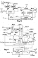
- FIG. 5 represents a stage for receiving UART circuit data including generator CKGEN2 clock according to the invention.
- the CKGEN2 generator receives a primary clock signal Ho of frequency Fo and period To, and delivers a clock signal of oversampling Hs of frequency Fs and period Ts as well as a clock signal bit Hb of frequency Fb and of period Tb.
- the integer part M1 of the setpoint M is identical to the setpoint M1 applied to a generator classic clock such as the CKGEN1 generator described upper.
- the setpoint M is delivered by a BDU unit ("Baud Rate Control Unit ”) responsible for determining the data transfer speed.
- BDU unit is in itself classic but here is authorized to issue a number decimal M after analysis of a synchronization character described above.
- This BDU unit is also not necessarily a synchronization unit using the SYNC character, and can be any type of loaded circuit check the value of the setpoint M supplied to the CKGEN2 generator.
- Setpoint M is loaded into two registers BRREG1, BRREG2 respectively receiving part M1 and the part M2, and the outputs of these registers are applied to the CKGEN2 generator.
- the generator CKGEN2 modulates the period of the pulses of the oversampling clock signal Hs, that is to say the duration separating two successive pulses from the clock signal Hs, so that the mean value Tsav of the period Ts of these pulses, over a determined number Ni of pulses, is substantially equal to To * M.
- the clock signal of oversampling Hs and bit clock signal Hb can be finely adjusted with a decimal divider M including numbers after the decimal point.
- the errors of synchronization are greatly reduced and brought back to the increment existing between two successive values of the decimal part M2.
- the rational number M2 can thus be adjusted between 0 and (M3max-1) / M3max in steps equal to 1 / M3max.
- M3max is preference equal to Ni (or N) and the increments of the decimal part M2 are equal to 1 / Ni (or 1 / N).
- the period Ts of the pulses of the clock signal Hs is modulated by discrete values near a value unmodulated and the numerator M3 of the rational number M2 determines the number of modulated periods.
- This discrete value modulation can be made of various ways and in particular according to one of the three methods mentioned below.
- Method 1 modulate the period of M3 pulses with a single modulation value equal to To * (M1 + 1) and choose as a non-modulated value a period of value To * M1.
- Method 2 modulate the period of M3 pulses with a single modulation value equal to To * (M1-1) and choose as a non-modulated value a period of value To * M1.
- Method 3 modulate the period of M3 pulses with two modulation values equal to To * (M1 + 1) and To (M1-1) and choose a period of value To * as unmodulated value M1.
- M3 is the numerator of a fraction M3 / M3max between -M3max / (2 * M3max) and (M3max-1) / (2 * M3max) either between -0.5 and (M3max-1) / (2 * M3max)), or between - (M3max-1) / (2 * M3max) and M3max / (2 * M3max) either between - (M3max-1) / (2 * M3max) and +0.5.
- the advantage of method 3 is that the number maximum of samples to be modulated in each group of Ni impulses is never greater than M3max / 2.
- FIG. 6 represents an exemplary embodiment of the CKGEN2 generator implementing method 3.
- M1 can be chosen between 1 and 255, i.e. an 8-bit M1 coding (register BRREG1).
- the clock generator includes a divider programmable DIV1 in 1 / M1 delivering the clock signal Hs, and a divider into 1 / N DIV2 delivering the signal clock bit Hb.
- the programmable divider DIV1 receives in input a variable division instruction MV delivered by a MODCT modulation circuit.
- MODCT circuit receives as input the integer part M1 of the setpoint M and is driven by a DISCT circuit.
- DIV1 divider includes DCT1 down counter programmable ("down-counter"), here of 8 bits, controlled by the primary clock signal Ho.
- the down counter DCT1 presents an input receiving the variable MV setpoint delivered by the MODCT modulation circuit. His exit is applied to an input of a COMP1 comparator receiving on its other input the value [00] h.
- the output of the DCT1 down-counter is also applied to an input of a COMP2 comparator receiving on its other entry the value [01] h. Leaving the COMP2 comparator delivers a LOAD loading signal a new variable MV setpoint after each cycle of countdown leading to the delivery of an impulse of the clock signal Hs.
- the DIV2 divider includes a DCT2 down counter by N, here of 4 bits, whose input receives the signal Hs.
- the output of this down counter is applied to an input of a COMP3 comparator receiving on its other input the value [00] h.
- the MODCT modulation circuit includes a MUX1 multiplexer receiving on a first input the whole part M1 of setpoint M and on a second input the whole part M1 decremented by one, that is M1-1.
- the value M1-1 is delivered by a block of DECB decrement receiving as input the whole part M1.
- the output of the multiplexer MUX1 is applied to a input of a MUX2 multiplexer from which the other input receives the integer part M1 incremented by one, i.e. M1 + 1.
- the value M1 + 1 is delivered by an increment block INCB receiving as input the output of the multiplexer MUX1 (or the whole part M1).
- variable setpoint MV can thus be equal to M1-1, M1 and M1 + 1. It follows that according to the value of the MV setpoint applied to divider DIV1 at the end of each countdown cycle, the period of the next pulse of the signal Hs can be equal to T0 * (M1-1), T0 * M1 or T0 * (M1 + 1).
- the multiplexers MUX1, MUX2 are controlled respectively by DEC, INC signals delivered by the DISCT circuit.
- the DISCT circuit is a distribution circuit of modulation which receives as input the numerator M3 of the decimal part M2, which is a rational number here M3 / M3max (M3max being predetermined here, only the numerator M3 is stored in the register BRREG2).
- the DISCT circuit distributes the modulation periods according to method 3 described above. Like a each group of N pulses the number of period Ts to modulate is never greater than M3max / 2, i.e. 8 periods to be modulated as much as possible, the DISCT module circuit preferably the period of the first and the last pulses without modulating the period of group central impulses (which define the samples taken into account for the value calculation majority).
- the rational number M2 is thus a fraction between -N / (2 (N-1)) and +0.5 or between -0.5 and + N / (2 (N-1)) in steps equal to 1 / N.
- coding convention we choose the following coding convention:
- the DISCT circuit receives a SCOUNT signal which indicates to it the rank of each pulse of the clock signal Hs at within each group of N pulses.
- the SCOUNT signal is here between 0 and 15 and is taken here at the output of the DCT2 down-counter, i.e. at the input of the comparator COMP 3.
- the DCT2 decounter is reset to zero at whenever an STB start bit is received by UART.
- the DCT2 down-counter receives a signal DET issued by the STBDET circuit (fig. 4), which changes to 1 when the STB bit is detected.
- the DISCT circuit is produced here by means of a VHDL compiler. Its structure is too complex to be illustrated by a logic diagram, we will describe below an example of a VHDL algorithm to achieve this circuit.
- VHDL algorithm for the compilation of the DISCT circuit VHDL algorithm for the compilation of the DISCT circuit:
- FIGs 7, 8 and 9 illustrate three examples of modulation of the signal pulse period Hs oversampling clock, chosen from the cases provided above.
- Hs oversampling clock chosen from the cases provided above.
- the length of the each pulse is mentioned in these figures, "Tosc" being the period of the primary clock signal (designated "To" in the above).
- Fsav is the frequency average of the signal Hs over a period of 16 periods.
- the present invention is moreover susceptible various applications in fields other than that asynchronous data transmissions, and is generally applicable to any type of circuit requiring fine adjustment of a clock signal, finding beyond the resolution capacity offered by a frequency division by an integer.
- the number Ni of periods for determining the average value of the period Ts can be a variable setpoint chosen by the user.
- the number Ni can also be chosen automatically by a circuit responsible for finding the best approximation, as a rational number M3 / Ni, and without exceeding a Nimax limit, of a setpoint including a purely decimal M2 part and not necessarily rational supplied to the generator clock according to the invention.
Landscapes
- Engineering & Computer Science (AREA)
- Theoretical Computer Science (AREA)
- Physics & Mathematics (AREA)
- General Engineering & Computer Science (AREA)
- General Physics & Mathematics (AREA)
- Dc Digital Transmission (AREA)
- Synchronisation In Digital Transmission Systems (AREA)
Abstract
Description
- la figure 1 précédemment décrite représente une liaison de données entre deux circuits UART,
- la figure 2 précédemment décrite représente le format classique de caractères asynchrones échangés par les circuits UART,
- la figure 3 précédemment décrite représente l'architecture d'un étage de réception de données de circuit UART et d'un générateur d'horloge classique,
- la figure 4 précédemment décrite représente une séquence de suréchantillonnage d'un bit permettant de déduire la valeur de ce bit par calcul de valeur majoritaire d'échantillons,
- la figure 5 représente un étage de réception de données de circuit UART comprenant un générateur d'horloge selon l'invention,
- la figure 6 représente un exemple de réalisation du générateur d'horloge selon l'invention, et
- les figures 7, 8 et 9 illustre des exemples de modulation de la période des impulsions d'un signal d'horloge délivré par le générateur d'horloge selon l'invention.
-- case "-8/16"
when M3 = "1000"
and SCOUNT = 13 or 12 or 11 or 10 or 3 or 2 or 1 or 0
or
-- case "-7/16"
when M3 = "1001"
and SCOUNT = 13 or 12 or 11 or 3 or 2 or 1 or 0
or
-- case "-6/16"
when M3 = "1010"
and SCOUNT = 13 or 12 or 11 or 2 or 1 or 0 or
-- case "-5/16"
when M3 = "1011"
and SCOUNT = 13 or 12 or 2 or 1 or 0
or
-- case "-4/16"
when M3 = "1100"
and SCOUNT = 13 or 12 or 1 or 0
or
-- case "-3/16"
when M3 = "1101"
and SCOUNT = 13 or 1 or 0
or
-- case "-2/16"
when M3 = "1110"
and SCOUNT = 13 or 0
or
-- case "-1/16"
when M3 = "1111"
and SCOUNT = 0
else '0'
***
INC = '1'
-- case "+1/16"
when M3 = "0001"
and SCOUNT = 13
or
-- case "+2/16"
when M3 = "0010"
and SCOUNT = 13 or 0
or
-- case "+3/16"
when M3 = "0011"
and SCOUNT = 13 or 12 or 0
or
-- case "+4/16"
when M3 = "0100"
and SCOUNT = 13 or 12 or 1 or 0
or
-- case "+5/16"
when M3 = "0101"
and SCOUNT = 13 or 12 or 11 or 1 or 0
-- case "+6/16"
when M3 = "0110"
and SCOUNT = 13 or 12 or 11 or 2 or 1 or 0
-- case "+7/16"
when M3 = 0111"
and SCOUNT = 13 or 12 or 11 or 10 or 2 or 1 or 0
else '0'
DEC = '1'
-- case "-8/16"
when M3 = "1000"
and SCOUNT = 13 or 12 or 11 or 10 or 3 or 2 or 1 or 0"
Claims (36)
- Générateur d'horloge programmable (CKGEN2) pour délivrer à partir d'un signal d'horloge primaire (Hs) de fréquence (Fo) et de période (To) déterminées un premier signal d'horloge (Hs) dont la fréquence (Fs) est égale à la fréquence (Fo) du signal d'horloge primaire divisée par une consigne M,
caractérisé en ce que la consigne M est un nombre décimal comprenant une partie entière M1 et une partie décimale M2, et en ce qu'il comprend des moyens (MODCT, DISCT, DIV1) pour moduler la période des impulsions du premier signal d'horloge de manière que la durée de Ni impulsions successives soit sensiblement égale à M*Ni fois la période (To) du signal d'horloge primaire (Ho), Ni étant un nombre de référence pour la modulation de la période des impulsions du premier signal d'horloge. - Générateur d'horloge selon la revendication 1, comprenant des moyens (DIV2) pour délivrer un second signal d'horloge (Hb) dont la fréquence (Fb) et est égale à la fréquence (Fs) du premier signal d'horloge (Hs) divisée par un nombre N.
- Générateur d'horloge selon la revendication 2, dans lequel Ni est égal à N.
- Générateur d'horloge selon l'une des revendications 1 à 3, dans lequel la partie décimale M2 de la consigne M est un nombre rationnel codé binaire représentant une fraction modulable par incréments égaux à 1/Ni.
- Générateur d'horloge selon la revendication 4, dans lequel la partie décimale M2 est une fraction comprise entre -(Ni-1)/(2*Ni) et +0,5 ou entre -0,5 et +(Ni-1)/(2*Ni) par incréments égaux à 1/Ni.
- Générateur d'horloge selon l'une des revendications 4 et 5, ne recevant en entrée que la partie entière M1 de la consigne et le numérateur (M3) de la partie décimale rationnelle M2 de la consigne.
- Générateur d'horloge selon l'une des revendications 1 à 6, comprenant des moyens (MODCT) de modulation de la période des impulsions du premier signal d'horloge, agencés pour délivrer des impulsions du premier signal d'horloge dont la. période (Ts) est égale à la période du signal d'horloge primaire (To) multipliée par un nombre entier (MV) dont la valeur est variable.
- Générateur d'horloge selon la revendication 7, dans lequel les moyens de modulation sont agencés pour délivrer des impulsions du premier signal d'horloge dont la période est modulée sur deux valeurs égales à M1*To et (M1+1)*To, To étant la période du signal d'horloge primaire (Ho).
- Générateur d'horloge selon la revendication 7, dans lequel les moyens de modulation sont agencés pour délivrer des impulsions du premier signal d'horloge dont la période est modulée sur deux valeurs égales à M1*To et (M1-1)*To, To étant la période du signal d'horloge primaire (Ho).
- Générateur d'horloge selon la revendication 7, dans lequel les moyens de modulation sont agencés pour délivrer des impulsions du premier signal d'horloge dont la période est modulée sur trois valeurs (M1-1)*To, M1*To et (M1+1)*To, To étant la période du signal d'horloge primaire (Ho).
- Générateur d'horloge selon l'une des revendications 7 à 10, dans lequel les moyens de modulation (MODCT) comprennent :un circuit multiplexeur (MUX1, MUX2) recevant en entrée plusieurs consignes de division (M1, M1-1, M1+1) dont la valeur varie par incréments entiers autour de la partie entière M1 de la consigne M, délivrant une consigne (MV) de valeur variable sélectionnée parmi les plusieurs consignes de division, etun diviseur (DIV1) de la fréquence du signal d'horloge primaire (Ho) recevant sur une entrée la consigne de valeur variable (MV) sélectionnée par le circuit multiplexeur.
- Générateur d'horloge selon l'une des revendications 7 à 11, dans lequel les moyens de modulation sont pilotés par un circuit de répartition de modulation (DISCT) agencé pour répartir d'une manière déterminée, sur un groupe de Ni impulsions successives, les impulsions ayant leur période modulée.
- Générateur d'horloge selon la revendication 12, dans lequel le circuit de répartition (DISCT) module en priorité la période des premières et des dernières impulsions parmi un groupe de Ni impulsions successives du premier signal d'horloge, et confère à la période des impulsions centrales du groupe de Ni impulsions une valeur non modulée.
- Générateur d'horloge selon l'une des revendications 12 et 13 dans lequel lorsque M2 est supérieur à 0, 5 le circuit de répartition module la période des impulsions du premier signal d'horloge par valeurs inférieures en utilisant comme valeur non modulée la valeur To*(M1+1), To étant la période du signal d'horloge primaire.
- Générateur d'horloge selon l'une des revendications 12 et 13, dans lequel lorsque M2 est inférieur à 0,5 le circuit de répartition module la période des impulsions du premier signal d'horloge par valeurs supérieures en utilisant comme valeur non modulée la valeur To*(M1), To étant la période du signal d'horloge primaire.
- Générateur d'horloge selon l'une des revendications 12 à 15, dans lequel le circuit de répartition (DISCT) comprend un bloc à logique câblée recevant en entrée la partie décimale M1 de la consigne M et délivrant aux moyens de modulation, à chaque nouvelle impulsion du premier signal d'horloge, un signal de sélection (DEC, INC) du nombre entier déterminant la période de l'impulsion du premier signal d'horloge.
- Circuit d'émission réception de données asynchrones (UART) comprenant un registre de suréchantillonnage (OSREG) relié à une borne de réception de données (Rx), le registre étant piloté par un signal d'horloge de suréchantillonnage (Hs), caractérisé en ce qu'il comprend un générateur d'horloge (CKGEN2) selon l'une des revendications 1 à 16 et en ce que le premier signal d'horloge (Hs) délivré par le générateur d'horloge forme le signal d'horloge de suréchantillonnage.
- Circuit d'émission réception de données selon la revendication 17, utilisant pour la réception ou l'émission de données un signal d'horloge bit (Hb). dont la fréquence (Fb) est égale à la fréquence (Fs) du premier signal d'horloge (Hs) divisée par le nombre de référence Ni (N) du'circuit générateur d'horloge.
- Procédé pour délivrer à partir d'un signal d'horloge primaire de fréquence (Fo) et de période (To) déterminées, un premier signal d'horloge dont la fréquence (Fs) est égale à la fréquence (Fo) du signal d'horloge primaire divisée par une consigne M, caractérisé en ce que la consigne M est un nombre décimal comprenant une partie entière M1 et une partie décimale M2, et en ce que la période des impulsions du premier signal d'horloge est modulée de manière que la durée de Ni impulsions successives soit sensiblement égale à M*Ni fois la période (To) du signal d'horloge primaire, Ni étant un nombre de référence pour la modulation de la période des impulsions du premier signal d'horloge.
- Procédé selon la revendication 19, comprenant la production d'un second signal d'horloge (Hb) dont la fréquence (Fb) est égale à la fréquence (Fs) du premier signal d'horloge (Hs) divisée par un nombre N.
- Procédé selon la revendication 20, dans lequel Ni est égal à N.
- Procédé selon l'une des revendications 19 à 21, dans lequel la partie décimale M2 de la consigne M est un nombre rationnel codé binaire représentant une fraction modulable par incréments égaux à 1/Ni.
- Procédé selon la revendication 22, dans lequel la partie décimale M2 est une fraction comprise entre - (Ni-1)/(2*Ni) et +0,5 ou entre -0,5 -et +(Ni-1)/(2*Ni) par incréments égaux à 1/Ni.
- Procédé selon l'une des revendications 22 et 23, dans lequel le codage du nombre rationnel M2 ne comprend que le codage du numérateur (M3) du nombre rationnel M2, dont le dénominateur (Ni, N, M3max) est un nombre prédéterminé.
- Procédé selon l'une des revendications 19 à 24, dans lequel la période des impulsions du premier signal d'horloge est modulée en multipliant la période du signal d'horloge primaire par un nombre entier dont la valeur est variable.
- Procédé selon la revendication 25, dans lequel la période des impulsions du premier signal d'horloge est modulée sur deux valeurs égales à M1*To et (M1+1)*To, To étant la période du signal d'horloge primaire (Ho).
- Procédé selon la revendication 25, dans lequel la période des impulsions du premier signal d'horloge est modulée sur deux valeurs égales à M1*To et (M1-1)*To, To étant la période du signal d'horloge primaire (Ho).
- Procédé selon la revendication 25, dans lequel la période des impulsions du premier signal d'horloge est modulée sur trois valeurs (M1-1)*To, M1*To et (M1+1)*To, To étant la période du signal d'horloge primaire (Ho).
- Procédé selon l'une des revendications 25 à 28, dans lequel la modulation de la période des impulsions du premier signal d'horloge est mise en oeuvre au moyen d'un circuit multiplexeur (MUX1, MUX2) recevant en entrée plusieurs consignes de division (M1-1, M1, M1+1) dont la valeur varie par incréments entiers autour de la partie entière M1 de la consigne M, et délivrant une consigne (MV) de valeur variable sélectionnée parmi les plusieurs consignes de division, et au moyen d'un diviseur (DIV1) de la fréquence du signal d'horloge primaire recevant sur une entrée la consigne de valeur variable (MV) sélectionnée par le circuit multiplexeur.
- Procédé selon l'une des revendications 25 à 29, dans lequel la modulation de la période des impulsions du premier signal d'horloge comprend une répartition de modulation consistant à répartir d'une manière déterminée, sur un groupe de Ni impulsions successives, les impulsions ayant leur période modulée.
- Procédé selon la revendication 30, dans lequel la répartition de modulation comprend le fait de moduler en priorité la période des premières et des dernières impulsions parmi un groupe de Ni impulsions successives, en conférant à la période des impulsions centrales du groupe une valeur non modulée.
- Procédé selon l'une des revendications 30 et 31 dans lequel lorsque M2 est supérieur à 0,5 la période des impulsions du premier signal d'horloge est modulée par valeurs inférieures en utilisant comme valeur non modulée la valeur To*(M1+1), To étant la période du signal d'horloge primaire (Ho).
- Procédé selon l'une des revendications 30 et 31, dans lequel lorsque M2 est inférieur à 0,5 la période des impulsions du premier signal d'horloge est modulée par valeurs supérieures en utilisant comme valeur non modulée la valeur To*(M1), To étant la période du signal d'horloge primaire (Ho).
- Procédé pour le suréchantillonnage, au moyen d'un signal d'horloge de suréchantillonnage (Hs), de données reçues sur une borne de réception de données, caractérisé en ce que le signal d'horloge de suréchantillonnage est délivré conformément au procédé selon l'une des revendications 19 à 33 à partir d'un signal d'horloge primaire de fréquence (Fo) et de période (To) déterminées.
- Procédé selon la revendication 34, comprenant la production d'un signal d'horloge bit (Hb) dont la fréquence (Fb) est égale à la fréquence (Fs) du signal d'horloge de suréchantillonnage (Hs) divisée par un nombre N.
- Procédé selon la revendication 35, dans lequel Ni=N.
Applications Claiming Priority (2)
| Application Number | Priority Date | Filing Date | Title |
|---|---|---|---|
| FR0212794A FR2845783A1 (fr) | 2002-10-15 | 2002-10-15 | Generateur d'horloge a consigne decimale et application d'un tel generateur d'horloge a un circuit uart |
| FR0212794 | 2002-10-15 |
Publications (1)
| Publication Number | Publication Date |
|---|---|
| EP1411412A1 true EP1411412A1 (fr) | 2004-04-21 |
Family
ID=32039739
Family Applications (1)
| Application Number | Title | Priority Date | Filing Date |
|---|---|---|---|
| EP03358014A Withdrawn EP1411412A1 (fr) | 2002-10-15 | 2003-10-10 | Générateur d'horloge à consigne décimale et application d'un tel générateur d'horloge à un circuit UART |
Country Status (3)
| Country | Link |
|---|---|
| US (1) | US7046065B2 (fr) |
| EP (1) | EP1411412A1 (fr) |
| FR (1) | FR2845783A1 (fr) |
Cited By (1)
| Publication number | Priority date | Publication date | Assignee | Title |
|---|---|---|---|---|
| CN101018052B (zh) * | 2006-02-10 | 2010-04-21 | 凌阳科技股份有限公司 | 一种时钟频率检测与转换装置 |
Families Citing this family (8)
| Publication number | Priority date | Publication date | Assignee | Title |
|---|---|---|---|---|
| JP5279170B2 (ja) * | 2006-03-28 | 2013-09-04 | セミコンダクター・コンポーネンツ・インダストリーズ・リミテッド・ライアビリティ・カンパニー | マスタ通信回路、スレーブ通信回路、及びデータ通信方法 |
| US9225240B2 (en) * | 2009-11-13 | 2015-12-29 | Macronix International Co., Ltd. | Charge pump utilizing external clock signal |
| WO2015058473A1 (fr) * | 2013-10-25 | 2015-04-30 | 深圳市明微电子股份有限公司 | Procédé et appareil de décodage de protocole de transmission et puce de décodage de protocole de transmission |
| CN103561008B (zh) * | 2013-10-25 | 2016-11-02 | 深圳市明微电子股份有限公司 | 一种传输协议解码方法、装置及传输协议解码芯片 |
| US9880965B2 (en) * | 2014-09-11 | 2018-01-30 | Qualcomm Incorporated | Variable frame length virtual GPIO with a modified UART interface |
| US9563398B2 (en) * | 2015-03-06 | 2017-02-07 | Qualcomm Incorporated | Impedance-based flow control for a two-wire interface system with variable frame length |
| US9971666B2 (en) | 2015-03-06 | 2018-05-15 | Qualcomm Incorporated | Technique of link state detection and wakeup in power state oblivious interface |
| DE102017201537B3 (de) * | 2017-01-31 | 2018-06-14 | Lenze Automation Gmbh | Schaltung zum Erzeugen eines Abtastsignals für eine UART-Schnittstelle und UART-Schnittstelle |
Citations (4)
| Publication number | Priority date | Publication date | Assignee | Title |
|---|---|---|---|---|
| US3976945A (en) * | 1975-09-05 | 1976-08-24 | Hewlett-Packard Company | Frequency synthesizer |
| JPH04235616A (ja) * | 1991-01-10 | 1992-08-24 | Murata Mach Ltd | クロック発生装置 |
| US5436628A (en) * | 1993-09-13 | 1995-07-25 | Intel Corporation | Programmable frequency timing generator with phase adjust |
| US6316982B1 (en) * | 1999-05-05 | 2001-11-13 | Texas Instruments Incorporated | Digital clock with controllable phase skew |
Family Cites Families (4)
| Publication number | Priority date | Publication date | Assignee | Title |
|---|---|---|---|---|
| US3928813A (en) | 1974-09-26 | 1975-12-23 | Hewlett Packard Co | Device for synthesizing frequencies which are rational multiples of a fundamental frequency |
| JP3086706B2 (ja) * | 1995-08-03 | 2000-09-11 | アンリツ株式会社 | ラショナル分周装置及びそれを用いる周波数シンセサイザ |
| US6441656B1 (en) * | 2001-07-31 | 2002-08-27 | Sun Microsystems, Inc. | Clock divider for analysis of all clock edges |
| JP3956768B2 (ja) * | 2002-05-14 | 2007-08-08 | ソニー株式会社 | クロック発生回路 |
-
2002
- 2002-10-15 FR FR0212794A patent/FR2845783A1/fr active Pending
-
2003
- 2003-10-10 EP EP03358014A patent/EP1411412A1/fr not_active Withdrawn
- 2003-10-14 US US10/684,823 patent/US7046065B2/en not_active Expired - Lifetime
Patent Citations (4)
| Publication number | Priority date | Publication date | Assignee | Title |
|---|---|---|---|---|
| US3976945A (en) * | 1975-09-05 | 1976-08-24 | Hewlett-Packard Company | Frequency synthesizer |
| JPH04235616A (ja) * | 1991-01-10 | 1992-08-24 | Murata Mach Ltd | クロック発生装置 |
| US5436628A (en) * | 1993-09-13 | 1995-07-25 | Intel Corporation | Programmable frequency timing generator with phase adjust |
| US6316982B1 (en) * | 1999-05-05 | 2001-11-13 | Texas Instruments Incorporated | Digital clock with controllable phase skew |
Non-Patent Citations (1)
| Title |
|---|
| PATENT ABSTRACTS OF JAPAN vol. 016, no. 586 (P - 1463) 25 December 1992 (1992-12-25) * |
Cited By (1)
| Publication number | Priority date | Publication date | Assignee | Title |
|---|---|---|---|---|
| CN101018052B (zh) * | 2006-02-10 | 2010-04-21 | 凌阳科技股份有限公司 | 一种时钟频率检测与转换装置 |
Also Published As
| Publication number | Publication date |
|---|---|
| FR2845783A1 (fr) | 2004-04-16 |
| US7046065B2 (en) | 2006-05-16 |
| US20040130361A1 (en) | 2004-07-08 |
Similar Documents
| Publication | Publication Date | Title |
|---|---|---|
| FR2869426A1 (fr) | Procede et circuit de generation de signaux d'horloge pour la communication par un bus serie | |
| FR2756688A1 (fr) | Circuit optique de pll et procede pour son controle | |
| FR2554994A1 (fr) | Dispositif de generation d'une frequence fractionnaire d'une frequence de reference | |
| FR2845783A1 (fr) | Generateur d'horloge a consigne decimale et application d'un tel generateur d'horloge a un circuit uart | |
| FR2652697A1 (fr) | Extracteur de donnees numeriques dans un signal video. | |
| FR2764139A1 (fr) | Dispositif de division de frequence a prediviseur suivi d'un compteur programmable, prediviseur et synthetiseur de frequence correspondants | |
| EP1101316B1 (fr) | Procede de recuperation d'horloge lors de l'echantillonnage de signaux de type numerique | |
| EP0134374B1 (fr) | Horloge à verrouillage de phase | |
| EP0452878B1 (fr) | Circuit de multiplexage de signaux d'horloge | |
| FR3133508A1 (fr) | Dispositif comportant un circuit de synchronisation pour realiser une communication en champ proche | |
| EP3048730B1 (fr) | Dispositif de synthèse de fréquence à boucle de rétroaction | |
| FR2618963A1 (fr) | Recepteur pour communication sur spectre disperse | |
| EP0473731B1 (fr) | Procede et dispositif de comparaison de deux signaux analogiques variables | |
| FR2695495A1 (fr) | Procédé et appareil de transfert de données fonctionnant à deux fréquences. | |
| EP3171183B1 (fr) | Procédé et dispositif de mesure de la fréquence d'un signal | |
| FR2573592A1 (fr) | Circuit oscillateur asservi en phase a un signal de frequence predeterminee | |
| EP0658838A1 (fr) | Dispositif de synthèse de fréquences | |
| EP1398900B1 (fr) | Transformation d'un signal périodique en un signal de fréquence ajustable | |
| EP1635501B1 (fr) | Procédé de détection du positionnement relatif de deux signaux et dispositif correspondant | |
| FR2463997A1 (fr) | Circuit permettant de deriver un signal de bits a cadence constante, a partir d'un signal numerique | |
| EP1411638A1 (fr) | Procédé et dispositif de génération d'un signal ayant une fréquence égale au produit d'une fréquence de référence par un nombre réel | |
| EP0328448B1 (fr) | Procédé et dispositif de synchronisation entre des terminaux communiquant par l'intermédiaire d'une chaîne n'assurant pas la transparence temporelle | |
| EP1052779A1 (fr) | Processeur ayant une fréquence de fonctionnement adaptable | |
| FR3168277A1 (fr) | Synchroniseur a frequence ajustee pour croisement de domaines d'horloge | |
| FR2746230A1 (fr) | Systeme de lissage d'une horloge a frequence non continue et son application a des transmissions asynchrones, notamment du type "atm" |
Legal Events
| Date | Code | Title | Description |
|---|---|---|---|
| PUAI | Public reference made under article 153(3) epc to a published international application that has entered the european phase |
Free format text: ORIGINAL CODE: 0009012 |
|
| AK | Designated contracting states |
Kind code of ref document: A1 Designated state(s): AT BE BG CH CY CZ DE DK EE ES FI FR GB GR HU IE IT LI LU MC NL PT RO SE SI SK TR |
|
| AX | Request for extension of the european patent |
Extension state: AL LT LV MK |
|
| 17P | Request for examination filed |
Effective date: 20040921 |
|
| AKX | Designation fees paid |
Designated state(s): DE FR GB IT |
|
| RAP1 | Party data changed (applicant data changed or rights of an application transferred) |
Owner name: STMICROELECTRONICS SA |
|
| STAA | Information on the status of an ep patent application or granted ep patent |
Free format text: STATUS: THE APPLICATION IS DEEMED TO BE WITHDRAWN |
|
| 18D | Application deemed to be withdrawn |
Effective date: 20100501 |