EP1406346B1 - Stripline parallel-series-fed proximity-coupled cavity backed patch antenna array - Google Patents
Stripline parallel-series-fed proximity-coupled cavity backed patch antenna array Download PDFInfo
- Publication number
- EP1406346B1 EP1406346B1 EP03077410A EP03077410A EP1406346B1 EP 1406346 B1 EP1406346 B1 EP 1406346B1 EP 03077410 A EP03077410 A EP 03077410A EP 03077410 A EP03077410 A EP 03077410A EP 1406346 B1 EP1406346 B1 EP 1406346B1
- Authority
- EP
- European Patent Office
- Prior art keywords
- antenna array
- distribution
- coupling
- trace
- elements
- Prior art date
- Legal status (The legal status is an assumption and is not a legal conclusion. Google has not performed a legal analysis and makes no representation as to the accuracy of the status listed.)
- Expired - Lifetime
Links
- 239000000758 substrate Substances 0.000 claims abstract description 51
- 230000008878 coupling Effects 0.000 claims abstract description 27
- 238000010168 coupling process Methods 0.000 claims abstract description 27
- 238000005859 coupling reaction Methods 0.000 claims abstract description 27
- 238000000034 method Methods 0.000 claims description 21
- 238000003491 array Methods 0.000 claims description 15
- 230000009977 dual effect Effects 0.000 claims description 7
- 238000005530 etching Methods 0.000 claims 1
- 238000010586 diagram Methods 0.000 description 6
- 230000001413 cellular effect Effects 0.000 description 5
- 238000004519 manufacturing process Methods 0.000 description 5
- 230000005855 radiation Effects 0.000 description 5
- 238000010276 construction Methods 0.000 description 4
- 238000004891 communication Methods 0.000 description 2
- 239000003989 dielectric material Substances 0.000 description 2
- 238000001228 spectrum Methods 0.000 description 2
- 230000003044 adaptive effect Effects 0.000 description 1
- 230000003321 amplification Effects 0.000 description 1
- 230000015572 biosynthetic process Effects 0.000 description 1
- 238000005388 cross polarization Methods 0.000 description 1
- 230000001934 delay Effects 0.000 description 1
- 238000009434 installation Methods 0.000 description 1
- 238000002955 isolation Methods 0.000 description 1
- 238000003199 nucleic acid amplification method Methods 0.000 description 1
Images

Classifications
-
- H—ELECTRICITY
- H01—ELECTRIC ELEMENTS
- H01Q—ANTENNAS, i.e. RADIO AERIALS
- H01Q21/00—Antenna arrays or systems
- H01Q21/0006—Particular feeding systems
- H01Q21/0075—Stripline fed arrays
-
- H—ELECTRICITY
- H01—ELECTRIC ELEMENTS
- H01Q—ANTENNAS, i.e. RADIO AERIALS
- H01Q21/00—Antenna arrays or systems
- H01Q21/0087—Apparatus or processes specially adapted for manufacturing antenna arrays
-
- H—ELECTRICITY
- H01—ELECTRIC ELEMENTS
- H01Q—ANTENNAS, i.e. RADIO AERIALS
- H01Q21/00—Antenna arrays or systems
- H01Q21/06—Arrays of individually energised antenna units similarly polarised and spaced apart
- H01Q21/061—Two dimensional planar arrays
- H01Q21/065—Patch antenna array
-
- H—ELECTRICITY
- H01—ELECTRIC ELEMENTS
- H01Q—ANTENNAS, i.e. RADIO AERIALS
- H01Q9/00—Electrically-short antennas having dimensions not more than twice the operating wavelength and consisting of conductive active radiating elements
- H01Q9/04—Resonant antennas
- H01Q9/0407—Substantially flat resonant element parallel to ground plane, e.g. patch antenna
- H01Q9/045—Substantially flat resonant element parallel to ground plane, e.g. patch antenna with particular feeding means
- H01Q9/0457—Substantially flat resonant element parallel to ground plane, e.g. patch antenna with particular feeding means electromagnetically coupled to the feed line
Definitions
- This invention generally relates to antennas, and more particularly to planar antenna arrays.
- a base station typically has a cellular tower and utilizes RF antennas that communicate with wireless devices, such as cellular phones and pagers.
- the base stations are linked with other facilities of the service provider, such as a switching or central office, for handling and processing the wireless communication traffic.
- a base station may be coupled to a processing facility through cables or wires, referred to as land lines, or alternatively, the signals may be transmitted or backhauled through microwave backhaul antennas, also located on the cellular tower and at the facility.
- Backhauls may be used in situations where land lines are unavailable or where a service provider faces an uncooperative local carrier and wants to ensure independent control of the circuit. In such a scenario, the backhaul may be referred to as a point-to-point backhaul, referencing the base station and the processing facility as points.
- Point-to-point backhauls are currently being deployed in the unlicensed spread spectrum bands, (e.g. Industrial, Scientific, and Medical (ISM) band covering 902-928 MHz, Unlicensed National Information Infrastructure band (U-NII) at 5.15-5.25 GHz, 5.25-5.35 GHz, and 5.725-5.825 GHz, etc.), to avoid the cost and time delays associated with installation in licensed frequency bands.
- ISM Industrial, Scientific, and Medical
- U-NII Unlicensed National Information Infrastructure band
- One type of antenna that may be used for point-to-point backhauls utilizes a parabolic dish that is mounted to a tower, a wall, a building or in another location, and aimed at the other point in the backhaul. Parabolic dishes are sometimes unsightly and spoil the aesthetic appearance of the location where they are mounted.
- Planar antenna arrays may also be mounted to a tower, a wall or a building, with the antenna being electrically pointed, i.e., via beamsteering, at the other point in the backhaul. Planar antenna arrays are generally thought of as more aesthetically appealing than parabolic dishes. Moreover, beamsteering makes planar antenna arrays more desirable in reconfiguring a cellular network. However, planar antenna arrays generally suffer from a variety of limitations.
- planar antennas arrays tend to be constructed using arrays of patch radiating elements.
- planar antennas may be constructed using printed circuit boards.
- these boards often utilize multiple layer construction techniques in order to form the elements and the feed networks used therewith. Such construction increases the cost of such boards.
- planar antennas constructed using arrays of patch radiating elements formed using multiple layer circuit boards typically use corporate feed networks for coupling the elements in the arrays.
- corporate feed networks are often in the form of microstrip or twin-lead feed lines deposited on one or more layers of a circuit board.
- Such corporate feed networks typically have high losses, while such microstrip or twin-lead feed lines typically result in poor cross-polarized performance of an antenna.
- multiple layer circuit boards may economically and/or practically limit the size of the antenna.
- current production capabilities of circuit board suppliers along with the production costs associated with constructing a circuit board larger than currently available, limit the size of multiple layer circuit boards.
- techniques of coupling two or more circuit boards together, thereby realizing a larger circuit board are largely thwarted as interconnection of multiple conductive layers in each board tends to be impractical.
- planar antennas constructed using such circuit boards may be limited in aperture size, i.e., the distance between the outer two most arrays of elements in an antenna, which determines in part the ability to electrically point the antenna.
- US-A-4,291,312 discloses a cavity-backed patch antenna array.
- planar antennas may reduce antenna performance, efficiency and increase amplification requirements, and may limit the ability to electrically point such an antenna.
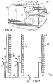
- FIG. 1 is a diagram showing an antenna array in accordance with the principles of the present invention.
- Figure 2 is diagram showing a cross section of a portion of one of the multi-layer substrates used in the antenna array of Figure 1 , taken through line 2-2.
- Figure 3 is a top view of a portion of one of the multi-layer substrates forming a proximity coupled cavity backed patch element used in the antenna array of Figure 1 .
- Figure 4 is a diagram of an exemplary distribution trace including a coupler extending along the inner conductive layer of the multi-layer substrate of Figure 2 and used in the antenna array of Figure 1 .
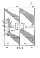
- Figure 5 is a diagram illustrating the assembly of the antenna array of Figure 1 .
- the present invention provides a stripline parallel-series fed proximity-coupled cavity backed patch antenna array.
- a stripline feed for improved isolation and cross-polarization for coupling proximity-coupled cavity backed microstrip patch elements, a large aperture antenna is provided using one or more multi-layer substrates.
- Such an antenna allows the use of adaptive beamforming for beamsteering and/or null forming thereby reducing susceptibility to other sources of radiation for applications such as a point-to-point microwave backhaul.
- FIG. 1 there is shown an exemplary stripline parallel-series fed proximity coupled cavity backed patch antenna array 10 for purposes of explaining the present invention.
- Antenna array 10 may be configured to provide a point-to-point backhaul in one of the unlicensed spread spectrum bands referred to hereinbefore.
- other embodiments of the present invention may be configured for other applications besides a point-to-point backhaul.
- embodiments of the present invention may be configured for operation in either other unlicensed or licensed frequency bands.
- Antenna array 10 comprises a plurality of multi-layer substrates 12a-d and a plurality of antenna elements 14 formed by the multi-layer substrates 12a-d.
- the antenna elements 14 may be proximity coupled cavity backed patch elements as illustrated.
- the antenna elements 14 may be formed in a series of columns 16, to allow beamsteering and/or null forming, and rows 18.
- Each multi-layer substrate 12a-d in Figure 1 includes twenty-one columns 16 containing twenty-one rows 18; thus, antenna array 10 comprises 42 columns and 42 rows.
- antenna array 10 comprises 42 columns and 42 rows.
- any number of columns and rows may be used without departing from the spirit of the present invention.
- an antenna array consistent with the present invention need not constitute rows per se.
- Each multi-layer substrate 12a-d is advantageously within current production capabilities of circuit board manufactures.
- the use of multi-layer substrates 12a-d facilitates an antenna of larger physical dimensions without incurring the costs associated with the production of a larger circuit board.
- the principles of the present invention apply equally to those larger circuit boards.
- embodiments of the present invention may use any number of multi-layer substrates as desired for economical and/or practical or other reasons. Further, the present invention need not constitute multiple substrates. Rather, embodiments of the present invention may use a single substrate should such a single substrate be desirable. Antenna array 10 merely uses four substrates 12a-d by way of example.
- array 10 facilitates a larger aperture size 20, defined by the distance across the series of columns 16.
- a larger aperture 20 increases beamsteering ability, thereby increasing the flexibility in mounting the antenna array 10.
- Each multi-layer substrate 12a-d is homogenous and mirrored in construction about the inner most edges of the substrates 12a-d, both horizontally and vertically, with respect to the other substrates 12a-d.
- Figures 2 and 3 refer to a cross section 22 and a portion 44 of multi-layer substrate 12a, respectively, whereas Figure 4 illustrates an inner conductive layer 28 of multi-layer substrate 12b.
- Figure 5 illustrates an inner conductive layer 28 of multi-layer substrate 12b.
- Cross-section 22 of multi-layer substrate 12a typifies the construction of multi-layer substrates 12a-d as, again, the multi-layer substrates 12a-d are homogeneous.
- Cross-section 22 is taken through an antenna element 14 for purposes of further illustrating the formation of an antenna element 14.
- Multi-layer substrate 12a comprises a top and bottom ground plane 24, 26 and an inner conductive layer 28, spaced by dielectric materials 30, 30' using techniques well know to those skilled in the art. Cut, etched or otherwise formed out of the top ground plane 24 is a radiating patch or patch 34. Multi-layer substrate 12a forms antenna element 14 by the element 14 including vias or plated through holes 32 connecting the top and bottom ground planes 24, 26 around a perimeter 36 (shown in Figure 3 ). The plated through holes 32 are spaced relative to one another so that they electromagnetically form a cavity 38, below radiating patch 34, at the operating frequency of the antenna element 14. Those skilled in the art will appreciate that the width of the wall of plated through holes 30 may be made less than half a guide or stub 42 wavelength thereby eliminating propagation of real power from the cavity 38 due to waveguide modes.
- the inner conductive layer 28 includes waveguide or stub 42 (shown in more detail in Figure 3 ) and a distribution trace 40 (shown in more detail in Figure 4 ).
- Stub 42 is located under patch 34 so that radiation from the stub 42 is contained within the cavity 38 and reradiated by the patch 34.
- Such an arrangement improves the front-to-back ratio performance of antenna array 10 " Experimental comparison of the Radiation Efficiency for Conventional and Cavity Backed Microstrip Antennas" by S. M. Duffy & M.M Gauker, 1996, IEEE Antennas and Propagation Society International Symposium 1996 Digest; Vol. 1, p 196-199 .
- Element 14 includes plated through holes 32 connecting the top and ground planes 24, 26 around the perimeter 36 of the element 14 forming a cavity 38, as described in conjunction with Figure 2 .
- the patch 34 and top layer of dielectric material 30, both of which were shown in Figure 2 have been removed to further illustrate stub 42.
- Stub 42 may advantageously be a dual three-quarter wavelength stub to achieve greater frequency variation. The dual three-quarter wavelength stub consisting of a common quarter wavelength line connected to two half wavelength stubs..
- Distribution trace 40 is a tapered trace, the width of which is readily varied by those skilled in the art to effectuate parameters such as impedance, power, phase, etc. of an electrical signal carried by the trace 40.
- Distribution trace 40 also includes a feed connection 52.
- Distribution trace 40 may be referred to as a "stripline" by virtue of being located between two ground planes 24, 26 (shown in Figure 2 ).
- distribution trace 40 includes a uniform power distribution portion 48 and a tapered power distribution portion 50 for coupling radiating elements 14 within a column 16.
- Uniform and tapered power distribution to radiating elements 14 within the sections 48, 50 is accomplished through varying the width of the trace 40 as will be readily understood by those skilled in the art. Due to varying the width of the trace 40 in portions 48, 50, the power received or transmitted by the elements 14 in those sections 48, 50 is apportioned as desired.
- those elements 14 in the uniform power distribution portion 48 may be referred to as connected in "parallel”
- those elements in the tapered power distribution portion may be referred to as being connected in "series”.
- distribution trace 40 may be referred to as a stripline parallel-series network that feeds proximity coupled cavity backed patch elements 14 in antenna array 10.
- Coupler 46 in the form of a trace 56.
- Coupler 46 includes a coupling connection 54.
- Coupler 46 may be optionally terminated with a load formed in trace 56, as indicated at reference numeral 58.
- Coupler 46 is formed by locating trace 56 proximate distribution trace 40 and adjacent a column 16.
- Coupling connection 54 allows a signal applied to the coupler 46 to vary, e.g. amplitude and/or phase, a signal applied through distribution trace 40 to a respective column 16.
- coupler 46 may be configured for beamforming, beamsteering and/or null forming antenna array 10.
- beamforming, beamsteering and/or null forming may be applied to any number or all of the columns 16 in antenna array 10, as desired.
- FIG. 5 a diagram showing the assembly of the antenna array 10 of Figure 1 is illustrated.
- multi-layer substrates 12a-d are shown from the side opposite that shown in Figure 1 , viewing bottom ground plane 26 as seen in Figure 2 . Areas in the bottom ground plane 26 have been etched away to facilitate feed connections 52 and coupling connections 54 formed in the inner conductive layer 28 shown in Figure 4 .
- feed connections 52 for all four multi-layer substrates 12a-d are shown, whereas coupling connections for only the outer most four columns 16 of multi-layer substrates 12a and 12d are shown.
- circuit boards 64, 66 are used for connections 52, 54, respectively.
- the circuit boards function to gather connections 52, 54 to reduce the number of cables that are needed for connection to antenna array 10.
- Circuit board 64 comprises a feed combiner 68 that connects to the feed connections 52 of each distribution trace 40 of each multi-layer substrate 12a-d and includes a main feed 60 for the antenna array 10.
- Circuit board 66 comprises coupling combiners 70 that connect couplers, within a respectively column 16, on multi-layer substrates 12a, 12d and provides column connections 70 for beamforming, beamsteering and/or null forming.
- Those skilled in the art will appreciate that other manners of gathering connections 52, 54 to reduce the number of cables that are needed for connection to antenna array may be used as desired.
Landscapes
- Engineering & Computer Science (AREA)
- Manufacturing & Machinery (AREA)
- Physics & Mathematics (AREA)
- Electromagnetism (AREA)
- Variable-Direction Aerials And Aerial Arrays (AREA)
- Waveguide Aerials (AREA)
- Details Of Aerials (AREA)
Applications Claiming Priority (2)
| Application Number | Priority Date | Filing Date | Title |
|---|---|---|---|
| US10/255,305 US6885343B2 (en) | 2002-09-26 | 2002-09-26 | Stripline parallel-series-fed proximity-coupled cavity backed patch antenna array |
| US255305 | 2002-09-26 |
Publications (3)
| Publication Number | Publication Date |
|---|---|
| EP1406346A2 EP1406346A2 (en) | 2004-04-07 |
| EP1406346A3 EP1406346A3 (en) | 2004-07-07 |
| EP1406346B1 true EP1406346B1 (en) | 2008-08-13 |
Family
ID=31993451
Family Applications (1)
| Application Number | Title | Priority Date | Filing Date |
|---|---|---|---|
| EP03077410A Expired - Lifetime EP1406346B1 (en) | 2002-09-26 | 2003-08-01 | Stripline parallel-series-fed proximity-coupled cavity backed patch antenna array |
Country Status (5)
| Country | Link |
|---|---|
| US (1) | US6885343B2 (https=) |
| EP (1) | EP1406346B1 (https=) |
| JP (1) | JP2004120733A (https=) |
| AT (1) | ATE405007T1 (https=) |
| DE (1) | DE60322810D1 (https=) |
Families Citing this family (21)
| Publication number | Priority date | Publication date | Assignee | Title |
|---|---|---|---|---|
| US20070080864A1 (en) * | 2005-10-11 | 2007-04-12 | M/A-Com, Inc. | Broadband proximity-coupled cavity backed patch antenna |
| US7692598B1 (en) * | 2005-10-26 | 2010-04-06 | Niitek, Inc. | Method and apparatus for transmitting and receiving time-domain radar signals |
| US7636063B2 (en) * | 2005-12-02 | 2009-12-22 | Eswarappa Channabasappa | Compact broadband patch antenna |
| US7652619B1 (en) | 2007-05-25 | 2010-01-26 | Niitek, Inc. | Systems and methods using multiple down-conversion ratios in acquisition windows |
| US7649492B2 (en) * | 2007-05-25 | 2010-01-19 | Niitek, Inc. | Systems and methods for providing delayed signals |
| US9316729B2 (en) * | 2007-05-25 | 2016-04-19 | Niitek, Inc. | Systems and methods for providing trigger timing |
| WO2009032496A2 (en) * | 2007-08-30 | 2009-03-12 | Commscope, Inc. Of North Carolina | Antenna with cellular and point-to-point communications capability |
| US7675454B2 (en) * | 2007-09-07 | 2010-03-09 | Niitek, Inc. | System, method, and computer program product providing three-dimensional visualization of ground penetrating radar data |
| US8207885B2 (en) * | 2007-09-19 | 2012-06-26 | Niitek, Inc. | Adjustable pulse width ground penetrating radar |
| US7642975B2 (en) * | 2008-03-12 | 2010-01-05 | Sikorsky Aircraft Corporation | Frame assembly for electrical bond |
| US20130285857A1 (en) * | 2011-10-26 | 2013-10-31 | John Colin Schultz | Antenna arrangement |
| US9843105B2 (en) | 2013-02-08 | 2017-12-12 | Honeywell International Inc. | Integrated stripline feed network for linear antenna array |
| KR102054200B1 (ko) * | 2013-11-20 | 2020-01-23 | 삼성전자주식회사 | 비아홀로 구성된, 캐비티-백 구조의 마이크로스트립 패치 안테나 |
| US9728855B2 (en) | 2014-01-14 | 2017-08-08 | Honeywell International Inc. | Broadband GNSS reference antenna |
| CN106067605B (zh) * | 2016-05-20 | 2018-09-21 | 北京华航无线电测量研究所 | 一种串馈微带阵列天线设计方法 |
| US11329393B2 (en) * | 2016-12-07 | 2022-05-10 | Fujikura Ltd. | Antenna device |
| US11205847B2 (en) * | 2017-02-01 | 2021-12-21 | Taoglas Group Holdings Limited | 5-6 GHz wideband dual-polarized massive MIMO antenna arrays |
| TWI705614B (zh) * | 2019-05-09 | 2020-09-21 | 和碩聯合科技股份有限公司 | 天線結構 |
| CN112186330A (zh) | 2019-07-03 | 2021-01-05 | 康普技术有限责任公司 | 基站天线 |
| TWI747457B (zh) * | 2020-08-24 | 2021-11-21 | 智易科技股份有限公司 | 用於抑制旁波瓣的增益的天線 |
| KR102914667B1 (ko) * | 2021-03-19 | 2026-01-19 | 삼성전자주식회사 | 안테나 구조 및 이를 포함하는 전자 장치 |
Family Cites Families (112)
| Publication number | Priority date | Publication date | Assignee | Title |
|---|---|---|---|---|
| US3728733A (en) | 1972-02-24 | 1973-04-17 | J Robinson | Beam antenna selectively oriented to vertical or horizontal position |
| US3731315A (en) | 1972-04-24 | 1973-05-01 | Us Navy | Circular array with butler submatrices |
| US3921177A (en) | 1973-04-17 | 1975-11-18 | Ball Brothers Res Corp | Microstrip antenna structures and arrays |
| GB1529361A (en) | 1975-02-17 | 1978-10-18 | Secr Defence | Stripline antenna arrays |
| US4032922A (en) | 1976-01-09 | 1977-06-28 | The United States Of America As Represented By The Secretary Of The Navy | Multibeam adaptive array |
| US4180817A (en) | 1976-05-04 | 1979-12-25 | Ball Corporation | Serially connected microstrip antenna array |
| US4291312A (en) * | 1977-09-28 | 1981-09-22 | The United States Of America As Represented By The Secretary Of The Navy | Dual ground plane coplanar fed microstrip antennas |
| US4197545A (en) * | 1978-01-16 | 1980-04-08 | Sanders Associates, Inc. | Stripline slot antenna |
| US4189675A (en) | 1978-05-30 | 1980-02-19 | Nasa | Satellite personal communications system |
| AU531239B2 (en) | 1978-06-15 | 1983-08-18 | Plessey Overseas Ltd. | Directional arrays |
| US4352202A (en) | 1979-09-04 | 1982-09-28 | Carney Richard E | Combined remote control for wireless communication equipment and associated antenna |
| US4246585A (en) | 1979-09-07 | 1981-01-20 | The United States Of America As Represented By The Secretary Of The Air Force | Subarray pattern control and null steering for subarray antenna systems |
| US4338605A (en) | 1980-02-28 | 1982-07-06 | Westinghouse Electric Corp. | Antenna array with adaptive sidelobe cancellation |
| US4287518A (en) | 1980-04-30 | 1981-09-01 | Nasa | Cavity-backed, micro-strip dipole antenna array |
| US4409595A (en) | 1980-05-06 | 1983-10-11 | Ford Aerospace & Communications Corporation | Stripline slot array |
| JPS5799803A (en) | 1980-12-12 | 1982-06-21 | Toshio Makimoto | Microstrip line antenna for circular polarized wave |
| US4394629A (en) | 1981-03-31 | 1983-07-19 | Rca Corporation | Hybrid power divider/combiner circuit |
| US4407001A (en) | 1981-10-02 | 1983-09-27 | The United States Of America As Represented By The Administrator Of The National Aeronautics And Space Administration | Focal axis resolver for offset reflector antennas |
| US4348253A (en) | 1981-11-12 | 1982-09-07 | Rca Corporation | Method for fabricating via holes in a semiconductor wafer |
| US4446463A (en) | 1982-02-24 | 1984-05-01 | The United States Of America As Represented By The Secretary Of The Navy | Coaxial waveguide commutation feed network for use with a scanning circular phased array antenna |
| US4686535A (en) | 1984-09-05 | 1987-08-11 | Ball Corporation | Microstrip antenna system with fixed beam steering for rotating projectile radar system |
| US4605931A (en) | 1984-09-14 | 1986-08-12 | The Singer Company | Crossover traveling wave feed for microstrip antenna array |
| JPS61167203A (ja) | 1985-01-21 | 1986-07-28 | Toshio Makimoto | 平面アンテナ |
| US4710775A (en) | 1985-09-30 | 1987-12-01 | The Boeing Company | Parasitically coupled, complementary slot-dipole antenna element |
| US4843402A (en) | 1986-06-27 | 1989-06-27 | Tri-Ex Tower Corporation | Azimuth array of rotory antennas with selectable lobe patterns |
| US4879711A (en) | 1986-08-14 | 1989-11-07 | Hughes Aircraft Company | Satellite communications system employing frequency reuse |
| IL82331A (en) | 1987-04-26 | 1991-04-15 | M W A Ltd | Microstrip and stripline antenna |
| US4849763A (en) | 1987-04-23 | 1989-07-18 | Hughes Aircraft Company | Low sidelobe phased array antenna using identical solid state modules |
| US4847626A (en) | 1987-07-01 | 1989-07-11 | Motorola, Inc. | Microstrip balun-antenna |
| FR2622055B1 (fr) | 1987-09-09 | 1990-04-13 | Bretagne Ctre Regl Innova Tran | Antenne plaque microonde, notamment pour radar doppler |
| US4972196A (en) | 1987-09-15 | 1990-11-20 | Board Of Trustees Of The Univ. Of Illinois | Broadband, unidirectional patch antenna |
| US4870421A (en) | 1987-12-28 | 1989-09-26 | General Electric Company | Regulating switch for transmitting modules in a phased array radar |
| US4806937A (en) | 1987-12-31 | 1989-02-21 | General Electric Company | Power distribution system for a phased array radar |
| US4833482A (en) | 1988-02-24 | 1989-05-23 | Hughes Aircraft Company | Circularly polarized microstrip antenna array |
| US4929959A (en) | 1988-03-08 | 1990-05-29 | Communications Satellite Corporation | Dual-polarized printed circuit antenna having its elements capacitively coupled to feedlines |
| US5412414A (en) | 1988-04-08 | 1995-05-02 | Martin Marietta Corporation | Self monitoring/calibrating phased array radar and an interchangeable, adjustable transmit/receive sub-assembly |
| US5117377A (en) | 1988-10-05 | 1992-05-26 | Finman Paul F | Adaptive control electromagnetic signal analyzer |
| DE3934155C2 (de) | 1988-10-13 | 1999-10-07 | Mitsubishi Electric Corp | Verfahren zum Messen einer Amplitude und einer Phase jedes Antennenelementes einer phasengesteuerten Antennenanordnung sowie Antennenanordnung zum Durchführen des Verfahrens |
| US5017931A (en) | 1988-12-15 | 1991-05-21 | Honeywell Inc. | Interleaved center and edge-fed comb arrays |
| JP2862265B2 (ja) | 1989-03-30 | 1999-03-03 | デイエツクスアンテナ株式会社 | 平面アンテナ |
| US5212494A (en) | 1989-04-18 | 1993-05-18 | Texas Instruments Incorporated | Compact multi-polarized broadband antenna |
| US4973972A (en) | 1989-09-07 | 1990-11-27 | The United States Of America As Represented By The Administrator Of The National Aeronautics And Space Adminstration | Stripline feed for a microstrip array of patch elements with teardrop shaped probes |
| US5233361A (en) | 1989-09-19 | 1993-08-03 | U.S. Philips Corporation | Planar high-frequency aerial for circular polarization |
| US4973971A (en) | 1989-12-18 | 1990-11-27 | Allied-Signal Inc. | Broadband circular phased array antenna |
| US5220335A (en) | 1990-03-30 | 1993-06-15 | The United States Of America As Represented By The Administrator Of The National Aeronautics And Space Administration | Planar microstrip Yagi antenna array |
| US5128687A (en) | 1990-05-09 | 1992-07-07 | The Mitre Corporation | Shared aperture antenna for independently steered, multiple simultaneous beams |
| US5019793A (en) | 1990-05-21 | 1991-05-28 | Hughes Aircraft Company | Digitally implemented variable phase shifter and amplitude weighting device |
| US5089823A (en) | 1990-11-30 | 1992-02-18 | Grumman Aerospace Corporation | Matrix antenna array |
| US5351060A (en) | 1991-02-25 | 1994-09-27 | Bayne Gerald A | Antenna |
| US5086302A (en) | 1991-04-10 | 1992-02-04 | Allied-Signal Inc. | Fault isolation in a Butler matrix fed circular phased array antenna |
| US5488380A (en) | 1991-05-24 | 1996-01-30 | The Boeing Company | Packaging architecture for phased arrays |
| US5160906A (en) | 1991-06-24 | 1992-11-03 | Motorola, Inc. | Microstripe filter having edge flared structures |
| US5248982A (en) | 1991-08-29 | 1993-09-28 | Hughes Aircraft Company | Method and apparatus for calibrating phased array receiving antennas |
| JP2765323B2 (ja) | 1991-12-12 | 1998-06-11 | 日本電気株式会社 | 追尾型アンテナ初期捕捉装置 |
| US5446471A (en) | 1992-07-06 | 1995-08-29 | Trw Inc. | Printed dual cavity-backed slot antenna |
| US5455594A (en) * | 1992-07-16 | 1995-10-03 | Conductus, Inc. | Internal thermal isolation layer for array antenna |
| US5757320A (en) | 1993-04-12 | 1998-05-26 | The Regents Of The University Of California | Short range, ultra-wideband radar with high resolution swept range gate |
| US5774091A (en) | 1993-04-12 | 1998-06-30 | The Regents Of The University Of California | Short range micro-power impulse radar with high resolution swept range gate with damped transmit and receive cavities |
| US5422649A (en) | 1993-04-28 | 1995-06-06 | The United States Of America As Represented By The Administrator Of The National Aeronautics And Space Administration | Parallel and series FED microstrip array with high efficiency and low cross polarization |
| US5485170A (en) | 1993-05-10 | 1996-01-16 | Amsc Subsidiary Corporation | MSAT mast antenna with reduced frequency scanning |
| US5461393A (en) | 1993-08-20 | 1995-10-24 | Texas Instruments Incorporated | Dual frequency cavity backed slot antenna |
| EP0649185B1 (en) | 1993-08-20 | 2000-04-12 | Raytheon Company | Improvements in or relating to antennas |
| US5633647A (en) | 1994-01-11 | 1997-05-27 | Tines; John L. | Base support for movable antenna |
| US5499005A (en) | 1994-01-28 | 1996-03-12 | Gu; Wang-Chang A. | Transmission line device using stacked conductive layers |
| GB9402942D0 (en) | 1994-02-16 | 1994-04-06 | Northern Telecom Ltd | Base station antenna arrangement |
| US5758287A (en) | 1994-05-20 | 1998-05-26 | Airtouch Communications, Inc. | Hub and remote cellular telephone system |
| US5724049A (en) | 1994-05-23 | 1998-03-03 | Hughes Electronics | End launched microstrip or stripline to waveguide transition with cavity backed slot fed by offset microstrip line usable in a missile |
| US5726664A (en) | 1994-05-23 | 1998-03-10 | Hughes Electronics | End launched microstrip or stripline to waveguide transition with cavity backed slot fed by T-shaped microstrip line or stripline usable in a missile |
| US6157343A (en) | 1996-09-09 | 2000-12-05 | Telefonaktiebolaget Lm Ericsson | Antenna array calibration |
| US5515057A (en) | 1994-09-06 | 1996-05-07 | Trimble Navigation Limited | GPS receiver with N-point symmetrical feed double-frequency patch antenna |
| US5512906A (en) | 1994-09-12 | 1996-04-30 | Speciale; Ross A. | Clustered phased array antenna |
| US5502372A (en) | 1994-10-07 | 1996-03-26 | Hughes Aircraft Company | Microstrip diagnostic probe for thick metal flared notch and ridged waveguide radiators |
| US5486835A (en) | 1994-10-31 | 1996-01-23 | University Corporation For Atmospheric Research | Low cost telemetry receiving system |
| US5663736A (en) | 1994-12-19 | 1997-09-02 | Rockwell International Corporation | Multi-element true time delay shifter for microwave beamsteering and beamforming |
| US5589843A (en) | 1994-12-28 | 1996-12-31 | Radio Frequency Systems, Inc. | Antenna system with tapered aperture antenna and microstrip phase shifting feed network |
| US5757246A (en) | 1995-02-27 | 1998-05-26 | Ems Technologies, Inc. | Method and apparatus for suppressing passive intermodulation |
| US5648786A (en) | 1995-11-27 | 1997-07-15 | Trw Inc. | Conformal low profile wide band slot phased array antenna |
| US5943016A (en) | 1995-12-07 | 1999-08-24 | Atlantic Aerospace Electronics, Corp. | Tunable microstrip patch antenna and feed network therefor |
| US5777581A (en) | 1995-12-07 | 1998-07-07 | Atlantic Aerospace Electronics Corporation | Tunable microstrip patch antennas |
| US5966102A (en) | 1995-12-14 | 1999-10-12 | Ems Technologies, Inc. | Dual polarized array antenna with central polarization control |
| US5767807A (en) | 1996-06-05 | 1998-06-16 | International Business Machines Corporation | Communication system and methods utilizing a reactively controlled directive array |
| WO1998011626A1 (en) | 1996-09-16 | 1998-03-19 | Raytheon Company | Antenna system for enhancing the coverage area, range and reliability of wireless base stations |
| US5856804A (en) | 1996-10-30 | 1999-01-05 | Motorola, Inc. | Method and intelligent digital beam forming system with improved signal quality communications |
| US5754138A (en) | 1996-10-30 | 1998-05-19 | Motorola, Inc. | Method and intelligent digital beam forming system for interference mitigation |
| US5754139A (en) | 1996-10-30 | 1998-05-19 | Motorola, Inc. | Method and intelligent digital beam forming system responsive to traffic demand |
| US6222503B1 (en) | 1997-01-10 | 2001-04-24 | William Gietema | System and method of integrating and concealing antennas, antenna subsystems and communications subsystems |
| US6115762A (en) | 1997-03-07 | 2000-09-05 | Advanced Micro Devices, Inc. | PC wireless communications utilizing an embedded antenna comprising a plurality of radiating and receiving elements responsive to steering circuitry to form a direct antenna beam |
| US6297774B1 (en) | 1997-03-12 | 2001-10-02 | Hsin- Hsien Chung | Low cost high performance portable phased array antenna system for satellite communication |
| SE510995C2 (sv) | 1997-03-24 | 1999-07-19 | Ericsson Telefon Ab L M | Aktiv sändnings/mottagnings gruppantenn |
| KR100207600B1 (ko) | 1997-03-31 | 1999-07-15 | 윤종용 | 공진기 부착형 마이크로스트립 다이폴 안테나 어레이 |
| US6081234A (en) | 1997-07-11 | 2000-06-27 | California Institute Of Technology | Beam scanning reflectarray antenna with circular polarization |
| US5940044A (en) | 1998-01-22 | 1999-08-17 | Allen Telecom Inc. | 45 degree polarization diversity antennas |
| DE69809704T2 (de) | 1998-02-12 | 2003-04-10 | Sony International (Europe) Gmbh | Antennen-Tragstruktur |
| US5905462A (en) | 1998-03-18 | 1999-05-18 | Lucent Technologies, Inc. | Steerable phased-array antenna with series feed network |
| US6025803A (en) | 1998-03-20 | 2000-02-15 | Northern Telecom Limited | Low profile antenna assembly for use in cellular communications |
| US6160522A (en) | 1998-04-02 | 2000-12-12 | L3 Communications Corporation, Randtron Antenna Systems Division | Cavity-backed slot antenna |
| FR2778272B1 (fr) | 1998-04-30 | 2000-09-08 | Alsthom Cge Alcatel | Dispositif de radiocommunication et antenne bifrequence realisee selon la technique des microrubans |
| US6133868A (en) | 1998-06-05 | 2000-10-17 | Metawave Communications Corporation | System and method for fully self-contained calibration of an antenna array |
| US6121936A (en) | 1998-10-13 | 2000-09-19 | Mcdonnell Douglas Corporation | Conformable, integrated antenna structure providing multiple radiating apertures |
| US6157340A (en) | 1998-10-26 | 2000-12-05 | Cwill Telecommunications, Inc. | Adaptive antenna array subsystem calibration |
| US6343208B1 (en) | 1998-12-16 | 2002-01-29 | Telefonaktiebolaget Lm Ericsson (Publ) | Printed multi-band patch antenna |
| US6157344A (en) | 1999-02-05 | 2000-12-05 | Xertex Technologies, Inc. | Flat panel antenna |
| US6292141B1 (en) | 1999-04-02 | 2001-09-18 | Qualcomm Inc. | Dielectric-patch resonator antenna |
| US6211824B1 (en) * | 1999-05-06 | 2001-04-03 | Raytheon Company | Microstrip patch antenna |
| US6300906B1 (en) | 2000-01-05 | 2001-10-09 | Harris Corporation | Wideband phased array antenna employing increased packaging density laminate structure containing feed network, balun and power divider circuitry |
| US6307525B1 (en) | 2000-02-25 | 2001-10-23 | Centurion Wireless Technologies, Inc. | Multiband flat panel antenna providing automatic routing between a plurality of antenna elements and an input/output port |
| US6335703B1 (en) | 2000-02-29 | 2002-01-01 | Lucent Technologies Inc. | Patch antenna with finite ground plane |
| US6445346B2 (en) * | 2000-04-27 | 2002-09-03 | Sarnoff Corporation | Planar polarizer feed network for a dual circular polarized antenna array |
| US6529166B2 (en) * | 2000-09-22 | 2003-03-04 | Sarnoff Corporation | Ultra-wideband multi-beam adaptive antenna |
| US6411258B1 (en) * | 2000-10-16 | 2002-06-25 | Andrew Corporation | Planar antenna array for point-to-point communications |
| TW478206B (en) | 2000-12-30 | 2002-03-01 | Hon Hai Prec Ind Co Ltd | Printed microstrip dipole antenna |
| US6583766B1 (en) * | 2002-01-03 | 2003-06-24 | Harris Corporation | Suppression of mutual coupling in an array of planar antenna elements |
-
2002
- 2002-09-26 US US10/255,305 patent/US6885343B2/en not_active Expired - Fee Related
-
2003
- 2003-08-01 DE DE60322810T patent/DE60322810D1/de not_active Expired - Lifetime
- 2003-08-01 EP EP03077410A patent/EP1406346B1/en not_active Expired - Lifetime
- 2003-08-01 AT AT03077410T patent/ATE405007T1/de not_active IP Right Cessation
- 2003-08-08 JP JP2003290759A patent/JP2004120733A/ja active Pending
Non-Patent Citations (2)
| Title |
|---|
| DELISLE J.T.; GOUKER M.A.; DUFFY S.M.: "45-GHZ MMIC POWER COMBINING USING A CIRCUIT-FED, SPATIALLY COMBINED ARRAY", IEEE MICROWAVE AND GUIDED WAVE LETTERS, vol. 7, no. 1, January 1997 (1997-01-01), NEW YORK, USA, pages 15 - 17, XP000636234 * |
| DUFFY S.M.; GOUKER M.A.: "Experimental comparison of the radiation efficiency for conventional and cavity backed microstrip antennas", IEEE ANTENNAS AND PROPAGATION SOCIETY INTERNATIONAL SYMPOSIUM. 1996 DIGEST., vol. 1, 1996, NEW YORK, USA, pages 196 - 199 * |
Also Published As
| Publication number | Publication date |
|---|---|
| JP2004120733A (ja) | 2004-04-15 |
| DE60322810D1 (de) | 2008-09-25 |
| EP1406346A3 (en) | 2004-07-07 |
| EP1406346A2 (en) | 2004-04-07 |
| US6885343B2 (en) | 2005-04-26 |
| US20040061647A1 (en) | 2004-04-01 |
| ATE405007T1 (de) | 2008-08-15 |
Similar Documents
| Publication | Publication Date | Title |
|---|---|---|
| EP1406346B1 (en) | Stripline parallel-series-fed proximity-coupled cavity backed patch antenna array | |
| US10673135B2 (en) | 5G terminal antenna with reconfigurable radiation pattern | |
| US10854994B2 (en) | Broadband phased array antenna system with hybrid radiating elements | |
| US7099686B2 (en) | Microstrip patch antenna having high gain and wideband | |
| EP1636873B1 (en) | Planar antenna for a wireless mesh network | |
| US7046201B2 (en) | Diversity antenna apparatus | |
| US9711860B2 (en) | Wideband antennas including a substrate integrated waveguide | |
| US20020190912A1 (en) | Planar high-frequency antenna | |
| US9112260B2 (en) | Microstrip antenna | |
| US20010050654A1 (en) | Printed circuit board-configured dipole array having matched impedance-coupled microstrip feed and parasitic elements for reducing sidelobes | |
| CN114256614A (zh) | 一种应用于毫米波通信系统的超宽带平面天线阵列 | |
| US6052098A (en) | Printed circuit board-configured dipole array having matched impedance-coupled microstrip feed and parasitic elements for reducing sidelobes | |
| CN110148828B (zh) | 天线单元和电子设备 | |
| CN116868442A (zh) | 包括耦合谐振结构层的低剖面设备 | |
| US6259416B1 (en) | Wideband slot-loop antennas for wireless communication systems | |
| KR102290591B1 (ko) | 밀리미터파 대역 무선 통신을 위한 스위치 빔포밍 안테나 장치 | |
| CN112768886B (zh) | 全向双极化天线和无线设备 | |
| CN116780180A (zh) | 毫米波封装滤波天线、天线阵列及无线通信设备 | |
| CN109449608B (zh) | 一种可提高天线间隔离度的微带阵列天线结构 | |
| US11394114B2 (en) | Dual-polarized substrate-integrated 360° beam steering antenna | |
| US10903569B2 (en) | Reconfigurable radial waveguides with switchable artificial magnetic conductors | |
| US20230136811A1 (en) | Antenna device, array of antenna devices, and base station | |
| Hastürkoğlu et al. | An automotive antenna set at 26.5 GHz for 5G-mobile communication | |
| CN113690575B (zh) | 一种应用于金属边框5g终端的三维波束覆盖毫米波天线 | |
| Temga et al. | 28GHz-band 2x2 patch antenna module vertically integrated with a compact 2-D BFN in broadside coupled stripline structure |
Legal Events
| Date | Code | Title | Description |
|---|---|---|---|
| PUAI | Public reference made under article 153(3) epc to a published international application that has entered the european phase |
Free format text: ORIGINAL CODE: 0009012 |
|
| AK | Designated contracting states |
Kind code of ref document: A2 Designated state(s): AT BE BG CH CY CZ DE DK EE ES FI FR GB GR HU IE IT LI LU MC NL PT RO SE SI SK TR |
|
| AX | Request for extension of the european patent |
Extension state: AL LT LV MK |
|
| PUAL | Search report despatched |
Free format text: ORIGINAL CODE: 0009013 |
|
| AK | Designated contracting states |
Kind code of ref document: A3 Designated state(s): AT BE BG CH CY CZ DE DK EE ES FI FR GB GR HU IE IT LI LU MC NL PT RO SE SI SK TR |
|
| AX | Request for extension of the european patent |
Extension state: AL LT LV MK |
|
| 17P | Request for examination filed |
Effective date: 20041215 |
|
| AKX | Designation fees paid |
Designated state(s): AT BE BG CH CY CZ DE DK EE ES FI FR GB GR HU IE IT LI LU MC NL PT RO SE SI SK TR |
|
| 17Q | First examination report despatched |
Effective date: 20050531 |
|
| 17Q | First examination report despatched |
Effective date: 20050531 |
|
| GRAP | Despatch of communication of intention to grant a patent |
Free format text: ORIGINAL CODE: EPIDOSNIGR1 |
|
| GRAS | Grant fee paid |
Free format text: ORIGINAL CODE: EPIDOSNIGR3 |
|
| GRAA | (expected) grant |
Free format text: ORIGINAL CODE: 0009210 |
|
| AK | Designated contracting states |
Kind code of ref document: B1 Designated state(s): AT BE BG CH CY CZ DE DK EE ES FI FR GB GR HU IE IT LI LU MC NL PT RO SE SI SK TR |
|
| REG | Reference to a national code |
Ref country code: GB Ref legal event code: FG4D |
|
| REG | Reference to a national code |
Ref country code: CH Ref legal event code: EP |
|
| REG | Reference to a national code |
Ref country code: IE Ref legal event code: FG4D |
|
| REF | Corresponds to: |
Ref document number: 60322810 Country of ref document: DE Date of ref document: 20080925 Kind code of ref document: P |
|
| PG25 | Lapsed in a contracting state [announced via postgrant information from national office to epo] |
Ref country code: NL Free format text: LAPSE BECAUSE OF FAILURE TO SUBMIT A TRANSLATION OF THE DESCRIPTION OR TO PAY THE FEE WITHIN THE PRESCRIBED TIME-LIMIT Effective date: 20080813 Ref country code: ES Free format text: LAPSE BECAUSE OF FAILURE TO SUBMIT A TRANSLATION OF THE DESCRIPTION OR TO PAY THE FEE WITHIN THE PRESCRIBED TIME-LIMIT Effective date: 20081124 |
|
| PG25 | Lapsed in a contracting state [announced via postgrant information from national office to epo] |
Ref country code: SI Free format text: LAPSE BECAUSE OF FAILURE TO SUBMIT A TRANSLATION OF THE DESCRIPTION OR TO PAY THE FEE WITHIN THE PRESCRIBED TIME-LIMIT Effective date: 20080813 Ref country code: AT Free format text: LAPSE BECAUSE OF FAILURE TO SUBMIT A TRANSLATION OF THE DESCRIPTION OR TO PAY THE FEE WITHIN THE PRESCRIBED TIME-LIMIT Effective date: 20080813 Ref country code: FI Free format text: LAPSE BECAUSE OF FAILURE TO SUBMIT A TRANSLATION OF THE DESCRIPTION OR TO PAY THE FEE WITHIN THE PRESCRIBED TIME-LIMIT Effective date: 20080813 |
|
| PG25 | Lapsed in a contracting state [announced via postgrant information from national office to epo] |
Ref country code: BE Free format text: LAPSE BECAUSE OF FAILURE TO SUBMIT A TRANSLATION OF THE DESCRIPTION OR TO PAY THE FEE WITHIN THE PRESCRIBED TIME-LIMIT Effective date: 20080813 |
|
| PG25 | Lapsed in a contracting state [announced via postgrant information from national office to epo] |
Ref country code: BG Free format text: LAPSE BECAUSE OF FAILURE TO SUBMIT A TRANSLATION OF THE DESCRIPTION OR TO PAY THE FEE WITHIN THE PRESCRIBED TIME-LIMIT Effective date: 20081113 Ref country code: DK Free format text: LAPSE BECAUSE OF FAILURE TO SUBMIT A TRANSLATION OF THE DESCRIPTION OR TO PAY THE FEE WITHIN THE PRESCRIBED TIME-LIMIT Effective date: 20080813 |
|
| PG25 | Lapsed in a contracting state [announced via postgrant information from national office to epo] |
Ref country code: PT Free format text: LAPSE BECAUSE OF FAILURE TO SUBMIT A TRANSLATION OF THE DESCRIPTION OR TO PAY THE FEE WITHIN THE PRESCRIBED TIME-LIMIT Effective date: 20090113 Ref country code: CZ Free format text: LAPSE BECAUSE OF FAILURE TO SUBMIT A TRANSLATION OF THE DESCRIPTION OR TO PAY THE FEE WITHIN THE PRESCRIBED TIME-LIMIT Effective date: 20080813 Ref country code: SK Free format text: LAPSE BECAUSE OF FAILURE TO SUBMIT A TRANSLATION OF THE DESCRIPTION OR TO PAY THE FEE WITHIN THE PRESCRIBED TIME-LIMIT Effective date: 20080813 Ref country code: RO Free format text: LAPSE BECAUSE OF FAILURE TO SUBMIT A TRANSLATION OF THE DESCRIPTION OR TO PAY THE FEE WITHIN THE PRESCRIBED TIME-LIMIT Effective date: 20080813 |
|
| PLBE | No opposition filed within time limit |
Free format text: ORIGINAL CODE: 0009261 |
|
| STAA | Information on the status of an ep patent application or granted ep patent |
Free format text: STATUS: NO OPPOSITION FILED WITHIN TIME LIMIT |
|
| 26N | No opposition filed |
Effective date: 20090514 |
|
| PG25 | Lapsed in a contracting state [announced via postgrant information from national office to epo] |
Ref country code: EE Free format text: LAPSE BECAUSE OF FAILURE TO SUBMIT A TRANSLATION OF THE DESCRIPTION OR TO PAY THE FEE WITHIN THE PRESCRIBED TIME-LIMIT Effective date: 20080813 |
|
| PG25 | Lapsed in a contracting state [announced via postgrant information from national office to epo] |
Ref country code: IT Free format text: LAPSE BECAUSE OF FAILURE TO SUBMIT A TRANSLATION OF THE DESCRIPTION OR TO PAY THE FEE WITHIN THE PRESCRIBED TIME-LIMIT Effective date: 20080813 |
|
| PGFP | Annual fee paid to national office [announced via postgrant information from national office to epo] |
Ref country code: FR Payment date: 20090814 Year of fee payment: 7 |
|
| PGFP | Annual fee paid to national office [announced via postgrant information from national office to epo] |
Ref country code: DE Payment date: 20090730 Year of fee payment: 7 Ref country code: GB Payment date: 20090729 Year of fee payment: 7 |
|
| PG25 | Lapsed in a contracting state [announced via postgrant information from national office to epo] |
Ref country code: SE Free format text: LAPSE BECAUSE OF FAILURE TO SUBMIT A TRANSLATION OF THE DESCRIPTION OR TO PAY THE FEE WITHIN THE PRESCRIBED TIME-LIMIT Effective date: 20081113 |
|
| PG25 | Lapsed in a contracting state [announced via postgrant information from national office to epo] |
Ref country code: MC Free format text: LAPSE BECAUSE OF NON-PAYMENT OF DUE FEES Effective date: 20090831 |
|
| REG | Reference to a national code |
Ref country code: CH Ref legal event code: PL |
|
| PG25 | Lapsed in a contracting state [announced via postgrant information from national office to epo] |
Ref country code: LI Free format text: LAPSE BECAUSE OF NON-PAYMENT OF DUE FEES Effective date: 20090831 Ref country code: CH Free format text: LAPSE BECAUSE OF NON-PAYMENT OF DUE FEES Effective date: 20090831 |
|
| PG25 | Lapsed in a contracting state [announced via postgrant information from national office to epo] |
Ref country code: IE Free format text: LAPSE BECAUSE OF NON-PAYMENT OF DUE FEES Effective date: 20090801 |
|
| PG25 | Lapsed in a contracting state [announced via postgrant information from national office to epo] |
Ref country code: GR Free format text: LAPSE BECAUSE OF FAILURE TO SUBMIT A TRANSLATION OF THE DESCRIPTION OR TO PAY THE FEE WITHIN THE PRESCRIBED TIME-LIMIT Effective date: 20081114 |
|
| GBPC | Gb: european patent ceased through non-payment of renewal fee |
Effective date: 20100801 |
|
| PG25 | Lapsed in a contracting state [announced via postgrant information from national office to epo] |
Ref country code: LU Free format text: LAPSE BECAUSE OF NON-PAYMENT OF DUE FEES Effective date: 20090801 |
|
| REG | Reference to a national code |
Ref country code: FR Ref legal event code: ST Effective date: 20110502 |
|
| REG | Reference to a national code |
Ref country code: DE Ref legal event code: R119 Ref document number: 60322810 Country of ref document: DE Effective date: 20110301 |
|
| PG25 | Lapsed in a contracting state [announced via postgrant information from national office to epo] |
Ref country code: HU Free format text: LAPSE BECAUSE OF FAILURE TO SUBMIT A TRANSLATION OF THE DESCRIPTION OR TO PAY THE FEE WITHIN THE PRESCRIBED TIME-LIMIT Effective date: 20090214 |
|
| PG25 | Lapsed in a contracting state [announced via postgrant information from national office to epo] |
Ref country code: FR Free format text: LAPSE BECAUSE OF NON-PAYMENT OF DUE FEES Effective date: 20100831 Ref country code: DE Free format text: LAPSE BECAUSE OF NON-PAYMENT OF DUE FEES Effective date: 20110301 |
|
| PG25 | Lapsed in a contracting state [announced via postgrant information from national office to epo] |
Ref country code: GB Free format text: LAPSE BECAUSE OF NON-PAYMENT OF DUE FEES Effective date: 20100801 Ref country code: TR Free format text: LAPSE BECAUSE OF FAILURE TO SUBMIT A TRANSLATION OF THE DESCRIPTION OR TO PAY THE FEE WITHIN THE PRESCRIBED TIME-LIMIT Effective date: 20080813 |
|
| PG25 | Lapsed in a contracting state [announced via postgrant information from national office to epo] |
Ref country code: CY Free format text: LAPSE BECAUSE OF FAILURE TO SUBMIT A TRANSLATION OF THE DESCRIPTION OR TO PAY THE FEE WITHIN THE PRESCRIBED TIME-LIMIT Effective date: 20080813 |