EP1406295A2 - Ein Verfahren zur Herstellung einer CMOS-Anordnung - Google Patents
Ein Verfahren zur Herstellung einer CMOS-Anordnung Download PDFInfo
- Publication number
- EP1406295A2 EP1406295A2 EP20030392011 EP03392011A EP1406295A2 EP 1406295 A2 EP1406295 A2 EP 1406295A2 EP 20030392011 EP20030392011 EP 20030392011 EP 03392011 A EP03392011 A EP 03392011A EP 1406295 A2 EP1406295 A2 EP 1406295A2
- Authority
- EP
- European Patent Office
- Prior art keywords
- region
- semiconductor substrate
- type
- silicon oxide
- underlying
- Prior art date
- Legal status (The legal status is an assumption and is not a legal conclusion. Google has not performed a legal analysis and makes no representation as to the accuracy of the status listed.)
- Withdrawn
Links
- 238000000034 method Methods 0.000 title claims abstract description 95
- 229910052814 silicon oxide Inorganic materials 0.000 claims abstract description 52
- 239000004065 semiconductor Substances 0.000 claims abstract description 50
- 239000000758 substrate Substances 0.000 claims abstract description 39
- 238000002513 implantation Methods 0.000 claims abstract description 31
- 239000012212 insulator Substances 0.000 claims abstract description 29
- 125000006850 spacer group Chemical group 0.000 claims abstract description 26
- 229920002120 photoresistant polymer Polymers 0.000 claims abstract description 17
- 229910021332 silicide Inorganic materials 0.000 claims abstract description 13
- FVBUAEGBCNSCDD-UHFFFAOYSA-N silicide(4-) Chemical compound [Si-4] FVBUAEGBCNSCDD-UHFFFAOYSA-N 0.000 claims abstract description 13
- 238000004519 manufacturing process Methods 0.000 claims abstract description 12
- 229910052751 metal Inorganic materials 0.000 claims abstract description 11
- 239000002184 metal Substances 0.000 claims abstract description 11
- 239000002131 composite material Substances 0.000 claims abstract description 8
- VYPSYNLAJGMNEJ-UHFFFAOYSA-N Silicium dioxide Chemical group O=[Si]=O VYPSYNLAJGMNEJ-UHFFFAOYSA-N 0.000 claims description 54
- 125000005843 halogen group Chemical group 0.000 claims description 34
- 229910052581 Si3N4 Inorganic materials 0.000 claims description 32
- HQVNEWCFYHHQES-UHFFFAOYSA-N silicon nitride Chemical compound N12[Si]34N5[Si]62N3[Si]51N64 HQVNEWCFYHHQES-UHFFFAOYSA-N 0.000 claims description 32
- -1 BF2 ions Chemical class 0.000 claims description 13
- 125000004429 atom Chemical group 0.000 claims description 12
- 229910044991 metal oxide Inorganic materials 0.000 claims description 9
- 150000004706 metal oxides Chemical class 0.000 claims description 9
- 238000004518 low pressure chemical vapour deposition Methods 0.000 claims description 8
- 229910052785 arsenic Inorganic materials 0.000 claims description 7
- RQNWIZPPADIBDY-UHFFFAOYSA-N arsenic atom Chemical compound [As] RQNWIZPPADIBDY-UHFFFAOYSA-N 0.000 claims description 7
- 238000000623 plasma-assisted chemical vapour deposition Methods 0.000 claims description 7
- ZOXJGFHDIHLPTG-UHFFFAOYSA-N Boron Chemical compound [B] ZOXJGFHDIHLPTG-UHFFFAOYSA-N 0.000 claims description 6
- 229910052796 boron Inorganic materials 0.000 claims description 6
- 238000005468 ion implantation Methods 0.000 claims description 6
- 235000012239 silicon dioxide Nutrition 0.000 claims description 6
- 239000000377 silicon dioxide Substances 0.000 claims description 6
- 229910021420 polycrystalline silicon Inorganic materials 0.000 claims description 4
- 229920005591 polysilicon Polymers 0.000 claims description 4
- 229910017052 cobalt Inorganic materials 0.000 claims description 3
- 239000010941 cobalt Substances 0.000 claims description 3
- GUTLYIVDDKVIGB-UHFFFAOYSA-N cobalt atom Chemical compound [Co] GUTLYIVDDKVIGB-UHFFFAOYSA-N 0.000 claims description 3
- 229910052715 tantalum Inorganic materials 0.000 claims description 3
- GUVRBAGPIYLISA-UHFFFAOYSA-N tantalum atom Chemical compound [Ta] GUVRBAGPIYLISA-UHFFFAOYSA-N 0.000 claims description 3
- QCWXUUIWCKQGHC-UHFFFAOYSA-N Zirconium Chemical compound [Zr] QCWXUUIWCKQGHC-UHFFFAOYSA-N 0.000 claims description 2
- 150000002500 ions Chemical class 0.000 claims description 2
- RUFLMLWJRZAWLJ-UHFFFAOYSA-N nickel silicide Chemical compound [Ni]=[Si]=[Ni] RUFLMLWJRZAWLJ-UHFFFAOYSA-N 0.000 claims description 2
- 229910021334 nickel silicide Inorganic materials 0.000 claims description 2
- 229910021341 titanium silicide Inorganic materials 0.000 claims description 2
- WQJQOUPTWCFRMM-UHFFFAOYSA-N tungsten disilicide Chemical compound [Si]#[W]#[Si] WQJQOUPTWCFRMM-UHFFFAOYSA-N 0.000 claims description 2
- 229910021342 tungsten silicide Inorganic materials 0.000 claims description 2
- 229910052726 zirconium Inorganic materials 0.000 claims description 2
- 238000000151 deposition Methods 0.000 claims 3
- 230000003647 oxidation Effects 0.000 claims 2
- 238000007254 oxidation reaction Methods 0.000 claims 2
- 230000000873 masking effect Effects 0.000 abstract description 15
- 230000015572 biosynthetic process Effects 0.000 abstract description 13
- 239000007943 implant Substances 0.000 abstract description 8
- 125000001475 halogen functional group Chemical group 0.000 abstract 2
- 238000004380 ashing Methods 0.000 description 5
- QVGXLLKOCUKJST-UHFFFAOYSA-N atomic oxygen Chemical compound [O] QVGXLLKOCUKJST-UHFFFAOYSA-N 0.000 description 5
- 229910052760 oxygen Inorganic materials 0.000 description 5
- 239000001301 oxygen Substances 0.000 description 5
- 239000002019 doping agent Substances 0.000 description 4
- PXHVJJICTQNCMI-UHFFFAOYSA-N Nickel Chemical compound [Ni] PXHVJJICTQNCMI-UHFFFAOYSA-N 0.000 description 2
- NBIIXXVUZAFLBC-UHFFFAOYSA-N Phosphoric acid Chemical compound OP(O)(O)=O NBIIXXVUZAFLBC-UHFFFAOYSA-N 0.000 description 2
- 238000005229 chemical vapour deposition Methods 0.000 description 2
- WEAMLHXSIBDPGN-UHFFFAOYSA-N (4-hydroxy-3-methylphenyl) thiocyanate Chemical compound CC1=CC(SC#N)=CC=C1O WEAMLHXSIBDPGN-UHFFFAOYSA-N 0.000 description 1
- XPDWGBQVDMORPB-UHFFFAOYSA-N Fluoroform Chemical compound FC(F)F XPDWGBQVDMORPB-UHFFFAOYSA-N 0.000 description 1
- XUIMIQQOPSSXEZ-UHFFFAOYSA-N Silicon Chemical compound [Si] XUIMIQQOPSSXEZ-UHFFFAOYSA-N 0.000 description 1
- RTAQQCXQSZGOHL-UHFFFAOYSA-N Titanium Chemical compound [Ti] RTAQQCXQSZGOHL-UHFFFAOYSA-N 0.000 description 1
- 229910000147 aluminium phosphate Inorganic materials 0.000 description 1
- 230000000903 blocking effect Effects 0.000 description 1
- 229910021419 crystalline silicon Inorganic materials 0.000 description 1
- 230000005669 field effect Effects 0.000 description 1
- 229910052759 nickel Inorganic materials 0.000 description 1
- 229910052710 silicon Inorganic materials 0.000 description 1
- 239000010703 silicon Substances 0.000 description 1
- 239000010936 titanium Substances 0.000 description 1
- 229910052719 titanium Inorganic materials 0.000 description 1
- WFKWXMTUELFFGS-UHFFFAOYSA-N tungsten Chemical compound [W] WFKWXMTUELFFGS-UHFFFAOYSA-N 0.000 description 1
- 229910052721 tungsten Inorganic materials 0.000 description 1
- 239000010937 tungsten Substances 0.000 description 1
- 238000007740 vapor deposition Methods 0.000 description 1
- 229910021355 zirconium silicide Inorganic materials 0.000 description 1
Images


Classifications
-
- H—ELECTRICITY
- H01—ELECTRIC ELEMENTS
- H01L—SEMICONDUCTOR DEVICES NOT COVERED BY CLASS H10
- H01L29/00—Semiconductor devices specially adapted for rectifying, amplifying, oscillating or switching and having potential barriers; Capacitors or resistors having potential barriers, e.g. a PN-junction depletion layer or carrier concentration layer; Details of semiconductor bodies or of electrodes thereof ; Multistep manufacturing processes therefor
- H01L29/66—Types of semiconductor device ; Multistep manufacturing processes therefor
- H01L29/66007—Multistep manufacturing processes
- H01L29/66075—Multistep manufacturing processes of devices having semiconductor bodies comprising group 14 or group 13/15 materials
- H01L29/66227—Multistep manufacturing processes of devices having semiconductor bodies comprising group 14 or group 13/15 materials the devices being controllable only by the electric current supplied or the electric potential applied, to an electrode which does not carry the current to be rectified, amplified or switched, e.g. three-terminal devices
- H01L29/66409—Unipolar field-effect transistors
- H01L29/66477—Unipolar field-effect transistors with an insulated gate, i.e. MISFET
- H01L29/66568—Lateral single gate silicon transistors
- H01L29/66575—Lateral single gate silicon transistors where the source and drain or source and drain extensions are self-aligned to the sides of the gate
- H01L29/6659—Lateral single gate silicon transistors where the source and drain or source and drain extensions are self-aligned to the sides of the gate with both lightly doped source and drain extensions and source and drain self-aligned to the sides of the gate, e.g. lightly doped drain [LDD] MOSFET, double diffused drain [DDD] MOSFET
- H01L29/66598—Lateral single gate silicon transistors where the source and drain or source and drain extensions are self-aligned to the sides of the gate with both lightly doped source and drain extensions and source and drain self-aligned to the sides of the gate, e.g. lightly doped drain [LDD] MOSFET, double diffused drain [DDD] MOSFET forming drain [D] and lightly doped drain [LDD] simultaneously, e.g. using implantation through the wings a T-shaped layer, or through a specially shaped layer
-
- H—ELECTRICITY
- H01—ELECTRIC ELEMENTS
- H01L—SEMICONDUCTOR DEVICES NOT COVERED BY CLASS H10
- H01L21/00—Processes or apparatus adapted for the manufacture or treatment of semiconductor or solid state devices or of parts thereof
- H01L21/70—Manufacture or treatment of devices consisting of a plurality of solid state components formed in or on a common substrate or of parts thereof; Manufacture of integrated circuit devices or of parts thereof
- H01L21/77—Manufacture or treatment of devices consisting of a plurality of solid state components or integrated circuits formed in, or on, a common substrate
- H01L21/78—Manufacture or treatment of devices consisting of a plurality of solid state components or integrated circuits formed in, or on, a common substrate with subsequent division of the substrate into plural individual devices
- H01L21/82—Manufacture or treatment of devices consisting of a plurality of solid state components or integrated circuits formed in, or on, a common substrate with subsequent division of the substrate into plural individual devices to produce devices, e.g. integrated circuits, each consisting of a plurality of components
- H01L21/822—Manufacture or treatment of devices consisting of a plurality of solid state components or integrated circuits formed in, or on, a common substrate with subsequent division of the substrate into plural individual devices to produce devices, e.g. integrated circuits, each consisting of a plurality of components the substrate being a semiconductor, using silicon technology
- H01L21/8232—Field-effect technology
- H01L21/8234—MIS technology, i.e. integration processes of field effect transistors of the conductor-insulator-semiconductor type
- H01L21/8238—Complementary field-effect transistors, e.g. CMOS
- H01L21/823814—Complementary field-effect transistors, e.g. CMOS with a particular manufacturing method of the source or drain structures, e.g. specific source or drain implants or silicided source or drain structures or raised source or drain structures
-
- H—ELECTRICITY
- H01—ELECTRIC ELEMENTS
- H01L—SEMICONDUCTOR DEVICES NOT COVERED BY CLASS H10
- H01L21/00—Processes or apparatus adapted for the manufacture or treatment of semiconductor or solid state devices or of parts thereof
- H01L21/70—Manufacture or treatment of devices consisting of a plurality of solid state components formed in or on a common substrate or of parts thereof; Manufacture of integrated circuit devices or of parts thereof
- H01L21/77—Manufacture or treatment of devices consisting of a plurality of solid state components or integrated circuits formed in, or on, a common substrate
- H01L21/78—Manufacture or treatment of devices consisting of a plurality of solid state components or integrated circuits formed in, or on, a common substrate with subsequent division of the substrate into plural individual devices
- H01L21/82—Manufacture or treatment of devices consisting of a plurality of solid state components or integrated circuits formed in, or on, a common substrate with subsequent division of the substrate into plural individual devices to produce devices, e.g. integrated circuits, each consisting of a plurality of components
- H01L21/822—Manufacture or treatment of devices consisting of a plurality of solid state components or integrated circuits formed in, or on, a common substrate with subsequent division of the substrate into plural individual devices to produce devices, e.g. integrated circuits, each consisting of a plurality of components the substrate being a semiconductor, using silicon technology
- H01L21/8232—Field-effect technology
- H01L21/8234—MIS technology, i.e. integration processes of field effect transistors of the conductor-insulator-semiconductor type
- H01L21/8238—Complementary field-effect transistors, e.g. CMOS
- H01L21/823828—Complementary field-effect transistors, e.g. CMOS with a particular manufacturing method of the gate conductors, e.g. particular materials, shapes
- H01L21/823835—Complementary field-effect transistors, e.g. CMOS with a particular manufacturing method of the gate conductors, e.g. particular materials, shapes silicided or salicided gate conductors
-
- H—ELECTRICITY
- H01—ELECTRIC ELEMENTS
- H01L—SEMICONDUCTOR DEVICES NOT COVERED BY CLASS H10
- H01L21/00—Processes or apparatus adapted for the manufacture or treatment of semiconductor or solid state devices or of parts thereof
- H01L21/70—Manufacture or treatment of devices consisting of a plurality of solid state components formed in or on a common substrate or of parts thereof; Manufacture of integrated circuit devices or of parts thereof
- H01L21/77—Manufacture or treatment of devices consisting of a plurality of solid state components or integrated circuits formed in, or on, a common substrate
- H01L21/78—Manufacture or treatment of devices consisting of a plurality of solid state components or integrated circuits formed in, or on, a common substrate with subsequent division of the substrate into plural individual devices
- H01L21/82—Manufacture or treatment of devices consisting of a plurality of solid state components or integrated circuits formed in, or on, a common substrate with subsequent division of the substrate into plural individual devices to produce devices, e.g. integrated circuits, each consisting of a plurality of components
- H01L21/822—Manufacture or treatment of devices consisting of a plurality of solid state components or integrated circuits formed in, or on, a common substrate with subsequent division of the substrate into plural individual devices to produce devices, e.g. integrated circuits, each consisting of a plurality of components the substrate being a semiconductor, using silicon technology
- H01L21/8232—Field-effect technology
- H01L21/8234—MIS technology, i.e. integration processes of field effect transistors of the conductor-insulator-semiconductor type
- H01L21/8238—Complementary field-effect transistors, e.g. CMOS
- H01L21/823864—Complementary field-effect transistors, e.g. CMOS with a particular manufacturing method of the gate sidewall spacers, e.g. double spacers, particular spacer material or shape
-
- H—ELECTRICITY
- H01—ELECTRIC ELEMENTS
- H01L—SEMICONDUCTOR DEVICES NOT COVERED BY CLASS H10
- H01L29/00—Semiconductor devices specially adapted for rectifying, amplifying, oscillating or switching and having potential barriers; Capacitors or resistors having potential barriers, e.g. a PN-junction depletion layer or carrier concentration layer; Details of semiconductor bodies or of electrodes thereof ; Multistep manufacturing processes therefor
- H01L29/66—Types of semiconductor device ; Multistep manufacturing processes therefor
- H01L29/66007—Multistep manufacturing processes
- H01L29/66075—Multistep manufacturing processes of devices having semiconductor bodies comprising group 14 or group 13/15 materials
- H01L29/66227—Multistep manufacturing processes of devices having semiconductor bodies comprising group 14 or group 13/15 materials the devices being controllable only by the electric current supplied or the electric potential applied, to an electrode which does not carry the current to be rectified, amplified or switched, e.g. three-terminal devices
- H01L29/66409—Unipolar field-effect transistors
- H01L29/66477—Unipolar field-effect transistors with an insulated gate, i.e. MISFET
- H01L29/6653—Unipolar field-effect transistors with an insulated gate, i.e. MISFET using the removal of at least part of spacer, e.g. disposable spacer
-
- H—ELECTRICITY
- H01—ELECTRIC ELEMENTS
- H01L—SEMICONDUCTOR DEVICES NOT COVERED BY CLASS H10
- H01L29/00—Semiconductor devices specially adapted for rectifying, amplifying, oscillating or switching and having potential barriers; Capacitors or resistors having potential barriers, e.g. a PN-junction depletion layer or carrier concentration layer; Details of semiconductor bodies or of electrodes thereof ; Multistep manufacturing processes therefor
- H01L29/66—Types of semiconductor device ; Multistep manufacturing processes therefor
- H01L29/68—Types of semiconductor device ; Multistep manufacturing processes therefor controllable by only the electric current supplied, or only the electric potential applied, to an electrode which does not carry the current to be rectified, amplified or switched
- H01L29/76—Unipolar devices, e.g. field effect transistors
- H01L29/772—Field effect transistors
- H01L29/78—Field effect transistors with field effect produced by an insulated gate
- H01L29/7833—Field effect transistors with field effect produced by an insulated gate with lightly doped drain or source extension, e.g. LDD MOSFET's; DDD MOSFET's
Definitions
- the present invention relates to methods used to fabricate semiconductor devices, and more specifically to a method used to form a high performance CMOS device at a lower fabrication cost as a result of reduced masking procedures.
- CMOS complementary metal oxide semiconductor
- NMOS N channel
- PMOS P channel
- the fabrication costs for CMOS devices however have remained extensive due to the numerous masking procedures needed.
- This invention will describe a novel fabrication sequence for a CMOS device in which performance increases are realized while the fabrication cost can be reduced when compared to counterpart CMOS devices achieved without the use of this present invention.
- the decrease in CMOS fabrication cost is achieved via a reduction in photolithographic masking steps.
- Novel procedures featuring disposable spacers allow several photolithographic masking steps that are used with counterpart CMOS devices fabricated without the use of this invention, to be eliminated.
- Prior art such as Pradeep et al, in U.S. Pat. No. 6,346,468 B1, Ang et al, in U.S. Pat. No. 6,319,783 B1, Pradeep et al, in U.S. Pat. No. 6,251,764 B1, Zhou et al, in U.S. Pat. No. 6,156,598, and Yu, in U.S. Pat. No. 6,348,387 B1, describe L - shaped spacers as well as lightly doped source/drain regions formed through L shaped spacers.
- MOSFET metal oxide semiconductor field effect
- It still yet another object of this invention to allow a process used to restore the partially removed spacer structure to allow a salicide procedure to be selectively performed in specific regions of the CMOS elements.
- a method of fabricating a CMOS device featuring a reduction in processing costs achieved via the reduction in photolithographic masking procedures, is described.
- a first insulator spacer comprised of an underlying silicon oxide layer and an overlying silicon nitride shape is formed on the sides of the gate structure.
- Removal of the silicon nitride shape results in a silicon oxide L shaped spacer comprised with a thick silicon oxide portion in a region underlying a previously removed silicon nitride shape, and comprised with a thinner silicon portion on regions exposed to the spacer definition and silicon nitride removal procedures.
- a series of implantation procedures are performed to form the halo, lightly doped source/drain (LDD), and heavily doped source/drain regions, for an exposed CMOS element.
- the halo region is formed using a high angle implantation, while a lower angle implantation procedure results in an LDD region underlying the thick silicon oxide portion, and results in a deeper, heavily doped source/drain region located underlying the thinner silicon oxide portion.
- the same procedure, block out mask, and series of implantation procedures are then used to form similar features for the previously blocked CMOS element.
- Semiconductor substrate 1 comprised of single crystalline silicon with a ⁇ 100> crystallographic orientation, is used and schematically shown in Fig. 1.
- First region 30, of semiconductor substrate 1 will be used to accommodate the NMOS element of a CMOS device, while second region 40, will be used to accommodate the PMOS element.
- a photoresist shape is used to protect NMOS region 30, from implantation of arsenic or phosphorous ions, used to form N well region 50, in a top portion of semiconductor substrate 1, in PMOS region 40.
- silicon dioxide gate insulator layer 2 is thermally grown to a thickness between about 10 to 100 Angstroms.
- a conductive layer such as a doped polysilicon layer, or a polycide layer comprised of a metal silicide layer on an underlying polysilicon layer, is next deposited via low pressure chemical vapor deposition (LPCVD) procedures, to a thickness between about 1000 to 3000 Angstroms.
- LPCVD low pressure chemical vapor deposition
- a photoresist shape is then used as an etch mask to allow an anisotropic reactive ion etch (RIE), procedure to define gate structures 3, using Cl 2 or SF 6 as an etchant for the conductive layer.
- the width of gate structures 3, is between about 0.05 to 10 um.
- the photoresist shape used to define gate structures 3, is next removed via a plasma oxygen ashing procedures, followed by a final wet clean cycle.
- the wet clean cycle features the use of a buffered hydrofluoric (BHF), step resulting in removal of the portions of silicon dioxide gate insulator layer not covered by gate structures 3. The result of these procedures is schematically shown in Fig. 1.
- Silicon oxide layer 4a is first deposited at a thickness between about 200 to 400 Angstroms via LPCVD or via plasma enhanced chemical vapor deposition (PECVD) procedures.
- Silicon nitride layer 5a shown schematically in Fig. 2, is now deposited via LPCVD or PECVD procedures to a thickness between about 500 to 800 Angstroms.
- An anisotropic RIE procedure using Cl 2 or CF 4 as an etchant for silicon nitride is employed to define silicon nitride shapes 5b, on underlying silicon oxide layer 4a.
- silicon oxide component 4c can be obtained via subjection to the anisotropic RIE procedure using CHF 3 as an etchant for silicon oxide, initiated directly after definition of silicon nitride shapes 5b. The result of this procedure is schematically shown in Fig. 3.
- L shaped silicon oxide spacers comprised of thick silicon oxide component 4b, located on the sides of gate structures 3, as well as on adjacent regions of the semiconductor substrate previously covered by the removed silicon nitride shapes 5b.
- the L shapes silicon oxide spacers are also comprised of thinner, silicon oxide component 4c, regions not previously covered by the removed silicon nitride shapes. The result of this procedure is schematically shown in Fig. 4.
- Photoresist shape 6 is next formed on PMOS region 40, and used as a block out mask to allow halo, LDD regions, and heavily doped source/drain regions, to be formed in specific locations in NMOS region 30.
- a halo region is employed to increase the dopant concentration in an area of the semiconductor substrate that will be used to accommodate a subsequent source/drain region.
- the higher dopant concentration provided by the halo region reduces the extent of the source/drain depletion region and thus reduces the risk of punch through, or leakage between depletion regions. Therefore the halo region has to be formed in a specific portion of the semiconductor substrate, allowing for containment of an entire source or drain region.
- an implantation procedure is performed using boron or BF 2 ions, at an energy between about 10 to 40 KeV, at a dose between about 1E13 to 1E15 atoms/cm 2 .
- a large implant angle between about 5 to 20° has to be used. The large implant angle allows the P type halo region to extend to a location underlying L shaped silicon oxide spacer 4b, as well as to a location underlying a portion of gate structure 3. This is schematically shown in Fig. 5.
- N type LDD region 8, and heavily doped N type source/drain region 9 are formed in regions of semiconductor substrate 1, not covered by gate structure 3, or by the vertical component of the L shaped silicon oxide spacer. This is accomplished via implantation of arsenic or phosphorous ions at an energy between about 1 to 10 KeV, at a dose between about 1E14 to 1E16 atoms/cm 2 , and via use of a low implant angle between about 0 to 7°.
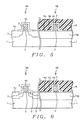
- photoresist shape 10 is formed on NMOS region 30, to protect this region from ion implantation procedures used to form the halo and source/drain regions for PMOS region 40.
- Halo region 11 is first formed via implantation of arsenic or phosphorous ions at an energy between about 80 to 150 KeV, at a dose between about 1E13 to 1E14 atoms/cm 2 , and again using a large implant angle between about 10 to 50°, needed to allow the N type halo region to form underlying a portion of the gate structure.
- the N type dopant concentration of halo region 11, is formed with a higher N type dopant concentration than that of N well region 50, to reduce source/drain punch through or leakage phenomena which can occur if P type source/drain depletion regions encroach.
- This is schematically illustrated in Fig. 7. With photoresist shape 10, still in place, P type LDD region 12, and heavily doped P type source/drain region 13, are formed in regions of semiconductor substrate 1, not covered by gate structure 3, or by the vertical component of L shaped silicon oxide spacer.
- silicon nitride layer 14a is deposited via LPCVD or PECVD procedures, to a thickness between about 200 to 800 Angstroms. This is schematically shown in Fig. 8. If a first group of devices require lower source/drain and gate resistance a self aligned silicide (salicide), procedure is employed, while a second group of devices not requiring lower resistance is protected from the salicide procedure. This is accomplished via protection of the second group of devices via use of a photoresist block out shape, while the first group of devices is subjected to a procedure allowing the gate structure and the source/drain regions to experience the salicide procedure.
- silicide silicide
- NMOS region 30 will be the first group of devices requiring low gate and source/drain resistance while PMOS region 40, will be the second group of devices not requiring the resistance lowering salicide procedure.
- Photoresist shape 15 is used as a block out mask allowing an anisotropic RIE procedure, using Cl 2 or CF 4 as an etchant to define silicon nitride shapes 14b, on the sides of, and overlying thick silicon oxide component 4b, in NMOS region 30. This is schematically shown in Fig. 9.
- a metal layer chosen from a group that contains titanium, tantalum, tungsten, nickel, cobalt, and zirconium, is next deposited via chemical vapor deposition (CVD), or via plasma vapor deposition (PVD), procedures, to a thickness between about 100 to 300 Angstroms.
- CVD chemical vapor deposition
- PVD plasma vapor deposition
- An anneal procedure is next performed either in a conventional furnace or via rapid thermal anneal (RTA) procedures, at a temperature between about 400 to 600° C, for a time between about 1 to 10 min, in an inert ambient, resulting in metal silicide formation on the exposed surfaces of gate structure 3, and heavily doped N type source/drain region 9, while unreacted metal remains on silicon nitride shapes 14b, and on silicon nitride layer 14a, in PMOS region 40.
- RTA rapid thermal anneal
- metal silicide layers 16 comprised of either titanium silicide, tantalum silicide, tungsten silicide, nickel silicide, cobalt silicide, and zirconium silicide. located on gate structure 3, and on heavily doped N type source/drain region 9.
Landscapes
- Engineering & Computer Science (AREA)
- Microelectronics & Electronic Packaging (AREA)
- Power Engineering (AREA)
- Physics & Mathematics (AREA)
- Condensed Matter Physics & Semiconductors (AREA)
- General Physics & Mathematics (AREA)
- Computer Hardware Design (AREA)
- Manufacturing & Machinery (AREA)
- Ceramic Engineering (AREA)
- Metal-Oxide And Bipolar Metal-Oxide Semiconductor Integrated Circuits (AREA)
- Insulated Gate Type Field-Effect Transistor (AREA)
- Electrodes Of Semiconductors (AREA)
Applications Claiming Priority (2)
| Application Number | Priority Date | Filing Date | Title |
|---|---|---|---|
| US262169 | 1994-06-20 | ||
| US10/262,169 US6762085B2 (en) | 2002-10-01 | 2002-10-01 | Method of forming a high performance and low cost CMOS device |
Publications (2)
| Publication Number | Publication Date |
|---|---|
| EP1406295A2 true EP1406295A2 (de) | 2004-04-07 |
| EP1406295A3 EP1406295A3 (de) | 2008-09-10 |
Family
ID=31993547
Family Applications (1)
| Application Number | Title | Priority Date | Filing Date |
|---|---|---|---|
| EP03392011A Withdrawn EP1406295A3 (de) | 2002-10-01 | 2003-09-30 | Ein Verfahren zur Herstellung einer CMOS-Anordnung |
Country Status (4)
| Country | Link |
|---|---|
| US (1) | US6762085B2 (de) |
| EP (1) | EP1406295A3 (de) |
| JP (1) | JP2004274022A (de) |
| SG (1) | SG111156A1 (de) |
Families Citing this family (34)
| Publication number | Priority date | Publication date | Assignee | Title |
|---|---|---|---|---|
| FR2846789B1 (fr) * | 2002-11-05 | 2005-06-24 | St Microelectronics Sa | Dispositif semi-conducteur a transistors mos a couche d'arret de gravure ayant un stress residuel ameliore et procede de fabrication d'un tel dispositif semi-conducteur |
| US7045408B2 (en) * | 2003-05-21 | 2006-05-16 | Intel Corporation | Integrated circuit with improved channel stress properties and a method for making it |
| US6905923B1 (en) * | 2003-07-15 | 2005-06-14 | Advanced Micro Devices, Inc. | Offset spacer process for forming N-type transistors |
| US6987061B2 (en) * | 2003-08-19 | 2006-01-17 | Texas Instruments Incorporated | Dual salicide process for optimum performance |
| US7018928B2 (en) * | 2003-09-04 | 2006-03-28 | Taiwan Semiconductor Manufacturing Co., Ltd. | Plasma treatment method to reduce silicon erosion over HDI silicon regions |
| US7135373B2 (en) * | 2003-09-23 | 2006-11-14 | Texas Instruments Incorporated | Reduction of channel hot carrier effects in transistor devices |
| TWI231989B (en) * | 2003-11-18 | 2005-05-01 | Promos Technologies Inc | Method of fabricating a MOSFET device |
| US7235848B2 (en) * | 2003-12-09 | 2007-06-26 | Applied Intellectual Properties Co., Ltd. | Nonvolatile memory with spacer trapping structure |
| US7049200B2 (en) * | 2004-05-25 | 2006-05-23 | Applied Materials Inc. | Method for forming a low thermal budget spacer |
| US7230296B2 (en) * | 2004-11-08 | 2007-06-12 | International Business Machines Corporation | Self-aligned low-k gate cap |
| JP4482428B2 (ja) * | 2004-11-12 | 2010-06-16 | 川崎マイクロエレクトロニクス株式会社 | 半導体集積回路の製造方法および半導体集積回路 |
| US7227234B2 (en) * | 2004-12-14 | 2007-06-05 | Tower Semiconductor Ltd. | Embedded non-volatile memory cell with charge-trapping sidewall spacers |
| US20060160317A1 (en) * | 2005-01-18 | 2006-07-20 | International Business Machines Corporation | Structure and method to enhance stress in a channel of cmos devices using a thin gate |
| US7858458B2 (en) | 2005-06-14 | 2010-12-28 | Micron Technology, Inc. | CMOS fabrication |
| JP4772456B2 (ja) * | 2005-11-04 | 2011-09-14 | 東京エレクトロン株式会社 | 半導体装置の製造方法、半導体装置の製造装置、制御プログラム及びコンピュータ記憶媒体 |
| US7759206B2 (en) * | 2005-11-29 | 2010-07-20 | International Business Machines Corporation | Methods of forming semiconductor devices using embedded L-shape spacers |
| US20070224745A1 (en) * | 2006-03-21 | 2007-09-27 | Hui-Chen Chang | Semiconductor device and fabricating method thereof |
| US7678636B2 (en) * | 2006-06-29 | 2010-03-16 | Taiwan Semiconductor Manufacturing Company, Ltd. | Selective formation of stress memorization layer |
| JP2008091536A (ja) | 2006-09-29 | 2008-04-17 | Toshiba Corp | 半導体装置及びその製造方法 |
| US7923373B2 (en) | 2007-06-04 | 2011-04-12 | Micron Technology, Inc. | Pitch multiplication using self-assembling materials |
| JP5096055B2 (ja) * | 2007-07-02 | 2012-12-12 | ローム株式会社 | Cmos型半導体集積回路の製造方法 |
| US8101479B2 (en) * | 2009-03-27 | 2012-01-24 | National Semiconductor Corporation | Fabrication of asymmetric field-effect transistors using L-shaped spacers |
| US8324110B2 (en) | 2010-02-02 | 2012-12-04 | International Business Machines Corporation | Field effect transistor (FET) and method of forming the FET without damaging the wafer surface |
| US8444255B2 (en) | 2011-05-18 | 2013-05-21 | Hewlett-Packard Development Company, L.P. | Power distribution in a thermal ink jet printhead |
| CN103187254B (zh) * | 2011-12-28 | 2015-12-02 | 北大方正集团有限公司 | 一种双多晶硅栅的制造方法 |
| US9508716B2 (en) * | 2013-03-14 | 2016-11-29 | Taiwan Semiconductor Manufacturing Company, Ltd. | Methods of manufacturing a semiconductor device |
| KR102050214B1 (ko) * | 2013-06-13 | 2019-12-02 | 삼성전자 주식회사 | 반도체 소자 제조 방법 |
| CN108630740B (zh) * | 2017-03-16 | 2021-07-09 | 中芯国际集成电路制造(上海)有限公司 | 半导体结构及其形成方法 |
| US10304683B2 (en) * | 2017-10-31 | 2019-05-28 | Globalfoundries Inc. | Early gate silicidation in transistor elements |
| US20220093740A1 (en) * | 2020-09-18 | 2022-03-24 | Qualcomm Incorporated | High-power field-effect transistor (fet) |
| CN112908855B (zh) * | 2021-01-28 | 2024-06-11 | 上海华力集成电路制造有限公司 | 一种提升p管组件负偏压温度不稳定性的方法 |
| US12034054B2 (en) * | 2021-03-25 | 2024-07-09 | Taiwan Semiconductor Manufacturing Company, Ltd. | Semiconductor device and method for forming the same |
| US11646353B1 (en) * | 2021-12-27 | 2023-05-09 | Nanya Technology Corporation | Semiconductor device structure |
| CN116169027A (zh) * | 2023-02-02 | 2023-05-26 | 武汉新芯集成电路制造有限公司 | 半导体装置的制作方法 |
Citations (5)
| Publication number | Priority date | Publication date | Assignee | Title |
|---|---|---|---|---|
| US4728617A (en) * | 1986-11-04 | 1988-03-01 | Intel Corporation | Method of fabricating a MOSFET with graded source and drain regions |
| GB2214349A (en) * | 1988-01-19 | 1989-08-31 | Standard Microsyst Smc | Process for fabricating mos devices |
| JPH05218078A (ja) * | 1992-02-03 | 1993-08-27 | Sharp Corp | 電界効果トランジスタの作製方法 |
| JPH06326122A (ja) * | 1993-05-17 | 1994-11-25 | Matsushita Electric Ind Co Ltd | Mos型半導体装置およびその製造方法 |
| US5757045A (en) * | 1996-07-17 | 1998-05-26 | Taiwan Semiconductor Manufacturing Company Ltd. | CMOS device structure with reduced risk of salicide bridging and reduced resistance via use of a ultra shallow, junction extension, ion implantation |
Family Cites Families (7)
| Publication number | Priority date | Publication date | Assignee | Title |
|---|---|---|---|---|
| EP0490535B1 (de) * | 1990-12-07 | 1996-08-21 | AT&T Corp. | Feldeffekttransistor mit inverser T-förmiger Silizid-Torelektrode |
| US6251764B1 (en) | 1999-11-15 | 2001-06-26 | Chartered Semiconductor Manufacturing Ltd. | Method to form an L-shaped silicon nitride sidewall spacer |
| US6319783B1 (en) | 1999-11-19 | 2001-11-20 | Chartered Semiconductor Manufatcuring Ltd. | Process to fabricate a novel source-drain extension |
| US6156598A (en) | 1999-12-13 | 2000-12-05 | Chartered Semiconductor Manufacturing Ltd. | Method for forming a lightly doped source and drain structure using an L-shaped spacer |
| US6346468B1 (en) | 2000-02-11 | 2002-02-12 | Chartered Semiconductor Manufacturing Ltd. | Method for forming an L-shaped spacer using a disposable polysilicon spacer |
| US6277683B1 (en) * | 2000-02-28 | 2001-08-21 | Chartered Semiconductor Manufacturing Ltd. | Method of forming a sidewall spacer and a salicide blocking shape, using only one silicon nitride layer |
| US6348387B1 (en) | 2000-07-10 | 2002-02-19 | Advanced Micro Devices, Inc. | Field effect transistor with electrically induced drain and source extensions |
-
2002
- 2002-10-01 US US10/262,169 patent/US6762085B2/en not_active Expired - Lifetime
-
2003
- 2003-09-25 SG SG200305764A patent/SG111156A1/en unknown
- 2003-09-30 EP EP03392011A patent/EP1406295A3/de not_active Withdrawn
- 2003-10-01 JP JP2003342753A patent/JP2004274022A/ja active Pending
Patent Citations (5)
| Publication number | Priority date | Publication date | Assignee | Title |
|---|---|---|---|---|
| US4728617A (en) * | 1986-11-04 | 1988-03-01 | Intel Corporation | Method of fabricating a MOSFET with graded source and drain regions |
| GB2214349A (en) * | 1988-01-19 | 1989-08-31 | Standard Microsyst Smc | Process for fabricating mos devices |
| JPH05218078A (ja) * | 1992-02-03 | 1993-08-27 | Sharp Corp | 電界効果トランジスタの作製方法 |
| JPH06326122A (ja) * | 1993-05-17 | 1994-11-25 | Matsushita Electric Ind Co Ltd | Mos型半導体装置およびその製造方法 |
| US5757045A (en) * | 1996-07-17 | 1998-05-26 | Taiwan Semiconductor Manufacturing Company Ltd. | CMOS device structure with reduced risk of salicide bridging and reduced resistance via use of a ultra shallow, junction extension, ion implantation |
Also Published As
| Publication number | Publication date |
|---|---|
| US20040063264A1 (en) | 2004-04-01 |
| SG111156A1 (en) | 2005-05-30 |
| US6762085B2 (en) | 2004-07-13 |
| JP2004274022A (ja) | 2004-09-30 |
| EP1406295A3 (de) | 2008-09-10 |
Similar Documents
| Publication | Publication Date | Title |
|---|---|---|
| US6762085B2 (en) | Method of forming a high performance and low cost CMOS device | |
| US6277683B1 (en) | Method of forming a sidewall spacer and a salicide blocking shape, using only one silicon nitride layer | |
| US5082794A (en) | Method of fabricating mos transistors using selective polysilicon deposition | |
| US5877041A (en) | Self-aligned power field effect transistor in silicon carbide | |
| US5744395A (en) | Low resistance, self-aligned, titanium silicide structures, using a single rapid thermal anneal procedure | |
| KR100199527B1 (ko) | 약하게 도핑된 드레인(ldd)형의 cmos장치제조방법 | |
| US6902980B2 (en) | Method of fabricating a high performance MOSFET device featuring formation of an elevated source/drain region | |
| US7898028B2 (en) | Process for fabricating a strained channel MOSFET device | |
| US6498067B1 (en) | Integrated approach for controlling top dielectric loss during spacer etching | |
| US6448167B1 (en) | Process flow to reduce spacer undercut phenomena | |
| JP2509518B2 (ja) | チタニウムシリサイドコンタクト製造方法 | |
| US6589836B1 (en) | One step dual salicide formation for ultra shallow junction applications | |
| US5773347A (en) | Method of maufacturing field effect transistor | |
| US5677217A (en) | Method for fabricating a mosfet device, with local channel doping and a titanium silicide gate | |
| US6815355B2 (en) | Method of integrating L-shaped spacers in a high performance CMOS process via use of an oxide-nitride-doped oxide spacer | |
| US5915181A (en) | Method for forming a deep submicron MOSFET device using a silicidation process | |
| US6969646B2 (en) | Method of activating polysilicon gate structure dopants after offset spacer deposition | |
| US6207492B1 (en) | Common gate and salicide word line process for low cost embedded DRAM devices | |
| US6368928B1 (en) | Method of forming an indium retrograde profile via use of a low temperature anneal procedure to reduce NMOS short channel effects | |
| TW445524B (en) | Method for forming raised source and drain | |
| US7084458B1 (en) | Semiconductor device having triple LDD structure and lower gate resistance formed with a single implant process | |
| US6627527B1 (en) | Method to reduce metal silicide void formation | |
| US6242312B1 (en) | Advanced titanium silicide process for very narrow polysilicon lines | |
| US5895244A (en) | Process to fabricate ultra-short channel nMOSFETs with self-aligned silicide contact | |
| US20060128106A1 (en) | Transistor and method for manufacturing thereof |
Legal Events
| Date | Code | Title | Description |
|---|---|---|---|
| PUAI | Public reference made under article 153(3) epc to a published international application that has entered the european phase |
Free format text: ORIGINAL CODE: 0009012 |
|
| AK | Designated contracting states |
Kind code of ref document: A2 Designated state(s): AT BE BG CH CY CZ DE DK EE ES FI FR GB GR HU IE IT LI LU MC NL PT RO SE SI SK TR |
|
| AX | Request for extension of the european patent |
Extension state: AL LT LV MK |
|
| RIN1 | Information on inventor provided before grant (corrected) |
Inventor name: ANG, CHEW HOE Inventor name: CHOOI, SIMON Inventor name: LIM, ENG HUA Inventor name: HSIA, LIANG CHOO Inventor name: SIAH, SOH YUN Inventor name: ZHENG, JIA ZHEN |
|
| RIN1 | Information on inventor provided before grant (corrected) |
Inventor name: ANG, CHEW HOE Inventor name: CHOOI, SIMON Inventor name: LIM, ENG HUA Inventor name: HSIA, LIANG CHOO Inventor name: SIAH, SOH YUN Inventor name: ZHENG, JIA ZHEN |
|
| PUAL | Search report despatched |
Free format text: ORIGINAL CODE: 0009013 |
|
| AK | Designated contracting states |
Kind code of ref document: A3 Designated state(s): AT BE BG CH CY CZ DE DK EE ES FI FR GB GR HU IE IT LI LU MC NL PT RO SE SI SK TR |
|
| AX | Request for extension of the european patent |
Extension state: AL LT LV MK |
|
| AKX | Designation fees paid | ||
| REG | Reference to a national code |
Ref country code: DE Ref legal event code: 8566 |
|
| STAA | Information on the status of an ep patent application or granted ep patent |
Free format text: STATUS: THE APPLICATION IS DEEMED TO BE WITHDRAWN |
|
| 18D | Application deemed to be withdrawn |
Effective date: 20090311 |