EP1406291A2 - Vorrichtung und Verfahren zur Elektronenstrahllithographie - Google Patents
Vorrichtung und Verfahren zur Elektronenstrahllithographie Download PDFInfo
- Publication number
- EP1406291A2 EP1406291A2 EP03022163A EP03022163A EP1406291A2 EP 1406291 A2 EP1406291 A2 EP 1406291A2 EP 03022163 A EP03022163 A EP 03022163A EP 03022163 A EP03022163 A EP 03022163A EP 1406291 A2 EP1406291 A2 EP 1406291A2
- Authority
- EP
- European Patent Office
- Prior art keywords
- electron beam
- target wafer
- compensation data
- beam lithography
- electron
- Prior art date
- Legal status (The legal status is an assumption and is not a legal conclusion. Google has not performed a legal analysis and makes no representation as to the accuracy of the status listed.)
- Withdrawn
Links
Images


Classifications
-
- H—ELECTRICITY
- H01—ELECTRIC ELEMENTS
- H01J—ELECTRIC DISCHARGE TUBES OR DISCHARGE LAMPS
- H01J37/00—Discharge tubes with provision for introducing objects or material to be exposed to the discharge, e.g. for the purpose of examination or processing thereof
- H01J37/30—Electron-beam or ion-beam tubes for localised treatment of objects
- H01J37/317—Electron-beam or ion-beam tubes for localised treatment of objects for changing properties of the objects or for applying thin layers thereon, e.g. for ion implantation
- H01J37/3174—Particle-beam lithography, e.g. electron beam lithography
-
- B—PERFORMING OPERATIONS; TRANSPORTING
- B82—NANOTECHNOLOGY
- B82Y—SPECIFIC USES OR APPLICATIONS OF NANOSTRUCTURES; MEASUREMENT OR ANALYSIS OF NANOSTRUCTURES; MANUFACTURE OR TREATMENT OF NANOSTRUCTURES
- B82Y10/00—Nanotechnology for information processing, storage or transmission, e.g. quantum computing or single electron logic
-
- B—PERFORMING OPERATIONS; TRANSPORTING
- B82—NANOTECHNOLOGY
- B82Y—SPECIFIC USES OR APPLICATIONS OF NANOSTRUCTURES; MEASUREMENT OR ANALYSIS OF NANOSTRUCTURES; MANUFACTURE OR TREATMENT OF NANOSTRUCTURES
- B82Y40/00—Manufacture or treatment of nanostructures
-
- H—ELECTRICITY
- H01—ELECTRIC ELEMENTS
- H01J—ELECTRIC DISCHARGE TUBES OR DISCHARGE LAMPS
- H01J37/00—Discharge tubes with provision for introducing objects or material to be exposed to the discharge, e.g. for the purpose of examination or processing thereof
- H01J37/30—Electron-beam or ion-beam tubes for localised treatment of objects
- H01J37/304—Controlling tubes by information coming from the objects or from the beam, e.g. correction signals
-
- H—ELECTRICITY
- H01—ELECTRIC ELEMENTS
- H01J—ELECTRIC DISCHARGE TUBES OR DISCHARGE LAMPS
- H01J2237/00—Discharge tubes exposing object to beam, e.g. for analysis treatment, etching, imaging
- H01J2237/30—Electron or ion beam tubes for processing objects
- H01J2237/304—Controlling tubes
- H01J2237/30455—Correction during exposure
- H01J2237/30461—Correction during exposure pre-calculated
Definitions
- the present invention relates to a lithography technique by an electron beam, and more particularly to an electron beam lithography system and an electron beam lithography method which are suitable for drawing circuit patterns on a semiconductor wafer.
- circuit-pattern formation technique As a kind of circuit-pattern formation technique, there is an electron beam lithography technique, which is broadly applied to the formation of circuit patterns on a semiconductor wafer in recent years. The problem of this technique is how to improve the accuracy of drawing.
- Factors which determine the accuracy of drawing include not only a disturbance caused by the surrounding environment but also the accuracy of target-wafer positioning provided by a stage, the accuracy of beam position control provided by an electron beam deflector, and deformation caused by a change in temperature of the target wafer.
- the change in temperature of the target wafer mainly means an increase in temperature.
- the increase in temperature is caused not only by external factors including heat generation of a coil of electromagnetic lens provided in electron beam applying apparatus, and frictional heat of a stage, but also by an internal factor, that is to say, an increase in temperature due to thermal energy given to a target wafer when an electron beam is applied to the target wafer to draw a pattern.
- the increase in temperature caused by the former namely the external factor
- the increase in temperature caused by the latter namely the internal factor
- the increase in temperature caused by the latter is a matter that is considerably difficult to be solved because in the first place the electron beam lithography system itself is based on the basic processing principle in which energy is given to a target wafer by an electron beam.
- the circuit patterns are drawn on a target wafer by use of the kinetic energy of an electron beam. Because the drawing accuracy of the electron beam is very high in comparison with a size of the target wafer, and is on the order of several nanometers, a discrepancy in position including thermal expansion of the target wafer becomes a major problem.
- thermal transmission to a target wafer is prevented by providing a stage of which heat generation is reduced, and by designing a cooling mechanism of the stage so that radiation of heat may be performed efficiently.
- the techniques for preventing thermal transmission to a target wafer are accompanied by the thermal interception to the target wafer.
- Such thermal interception conversely results in a larger influence on the increase in temperature and the thermal expansion which are caused by energy directly given to the target wafer at the time of the electron beam lithography. It is because heat generated by an electron beam is kept in an area around a target holder, hindering diffusion of thermal energy of the target wafer.
- This problem can be improved by providing a heat dissipation mechanism, for instance, by providing a stage with a pipe of coolant.
- a heat dissipation mechanism for instance, by providing a stage with a pipe of coolant.
- providing such a mechanism does not reach an ultimate solution because a bottleneck is produced in the design in which the target holder must not be in contact with other parts, and further because a delay caused by the cooling, and stability of temperature of coolant, become new problems.
- the influence of the thermal expansion of the target wafer is reduced by measuring a temperature of the target wafer, and by providing a reference point on the target wafer so that it becomes possible to draw a circuit pattern with reference to the reference point , and further by determining the total amount of energy given to the target wafer to calculate the absolute temperature of the target wafer so that the extent of the thermal expansion of the target wafer is measured and estimated (for example, refers to patent document 1).
- An object of the present invention is to provide an electron beam lithography system and an electron beam lithography method that reduce the influence on drawing discrepancy caused by thermal expansion of a target wafer, and that thereby easily achieve high accuracy drawing.
- an electron beam lithography system of a type in which an electron beam is scanned according to a predetermined drawing program to draw circuit patterns on a target wafer comprising:
- an electron beam lithography system of a type in which an electron beam is scanned according to a drawing program that is predetermined but can also be changed to draw circuit patterns on a target wafer, the system comprising:
- said calculating means may also calculate the compensation data by means of computer simulation.
- an electron beam lithography method of a type in which an electron beam is scanned according to a predetermined drawing program to draw circuit patterns on a target wafer comprising the steps of:
- an electron beam lithography system of a type in which.an electron beam is scanned according to a drawing program that is predetermined but can also be changed to draw circuit patterns on a target wafer, said method comprising the steps of:
- said step for calculating the compensation data may also be a step for calculating the compensation data by means of computer simulation.
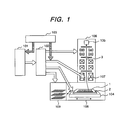
- Fig. 1 is a diagram illustrating one embodiment according to the present invention.
- reference numeral 106 denotes an electro-optic system
- reference numeral 108 denotes a target loader. In a broad sense, they constitute the electron beam lithography system.
- reference numeral 1 is a target, that is to say, a semiconductor wafer on which, for example, circuit patterns are drawn according to a predetermined drawing program.
- This target wafer 1 is held on a target holder 2, and is positioned by a stage 104. At this time, the target holder 2 is housed in a vacuum chamber 108 that totally communicates with a target loader (loader) 109 and the electro-optic system 106.
- a target loader loader
- a control computer 101 controls the stage 104, the electro-optic system 106, and the target loader 108 through a control system 102 according to a predetermined drawing program. Because the control system 102 includes a power supply system, the control system 102 also has a function of providing the electro-optic system 106 with power supply required for operation.
- the electro-optic system 106 includes a beam converging means for focusing an electron beam 3 emitted from an electron source 105 by use of an electromagnetic lens, and a beam scanning unit 107 for scanning an electron-beam applying position on the target wafer 1.
- the electro-optic system 106 therefore, has a function of applying the electron beam to the target wafer 1 to draw circuit patterns, or the like, according to a predetermined drawing program.
- the amount of deflection which is calculated from a dose and an applying position of the electron beam by use of a thermal-deformation calculating computer 103 is used as the amount of compensation. This is a feature of this embodiment. How to calculate the amount of deflection will be described as below.
- the heat which is given to the target wafer 1 by the electron beam 105 causes thermal expansion of the target wafer 1, leading to three kinds of deformation mentioned below, each of which produces a discrepancy in position to which an electron beam is applied.
- the three kinds of deformation include parallel expansion, non-parallel expansion, and 3-dimensional deformation (bend or curvature), which will be specifically described as below.
- the parallel expansion is a phenomenon in which thermal energy uniformly spreads through the whole target wafer, causing the target wafer to expand as a whole and consequently to grow in planar size.
- the thermal expansive force of a crystal forming the target wafer is in general stronger than the force that secures the target wafer to a stage. Therefore, even if the target wafer is secured, it is difficult to compulsorily prevent the discrepancy caused by the thermal expansion from occurring.
- a moving distance, and its direction, of the movement caused at certain time by the thermal expansion at a point where a pattern should be drawn on the target wafer 1 by an electron beam are uniquely determined by a relative position of the drawing position relative to the fixing point, and by an integrated value of the thermal energy which has been given to the target wafer 1 by the electron beam.
- the non-parallel expansion is a phenomenon in which thermal energy is locally given to a target wafer, resulting in uneven thermal expansion of the target wafer, and causing a plane shape to change.
- the target wafer 1 has thermal conductivity. As shown in Fig. 3, the thermal energy which has been given to a part of the target wafer 1 (part 302) by use of an electron beam spreads through the whole target wafer 1 in a finite period of time.
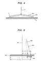
- the 3-dimensional deformation means a phenomenon in which if thermal energy given by an electron beam stays near a surface of the target wafer that is relatively thick, its thermal expansion differs between the front surface and the back surface, and consequently, as shown in Fig. 4, the target wafer bends backward, causing an area around an applying position of the electron beam 3 (a central part in the figure) to be deformed in a direction away from the stage.
- the temperature distribution on the target wafer is acquired using a simulation model. This means will be described as below.
- the thermal balance of the target wafer is limited to three kinds of processes, that is to say, application of energy by an electron beam, diffusion of the energy through the whole target wafer, and thermal transmission by radiation into a target chamber.
- the electron beam applied to the target wafer gives energy to a narrow range of area around an electron-beam applied part of the target wafer, and most of the energy is then absorbed in the target wafer.
- An applying position, applying time, and applying intensity of this electron beam are provided beforehand to the electron beam lithography system in a form of data containing a program as drawing patterns to be drawn on the target wafer. Accordingly, they are completely predictable.
- Process 2 Diffusion of the energy through the whole target wafer
- the target wafer is well thermal-insulated, a difference in temperature in the target wafer is caused by the thermal energy imbalance in the target wafer. Then, in response to thermal gradient and thermal conductivity of the target wafer, and according to the well-known diffusion equation, the energy spreads out in directions that lessen the difference in temperature.
- the target wafer heated by the electron beam is placed in the vacuum target chamber, the target wafer loses the energy mainly due to radiation, and therefore slowly reaches a thermal equilibrium state.
- This process can be expressed by a quantum mechanical equation based on the assumption of black body radiation that depends on a surface temperature. The equation enables estimation with sufficient accuracy as correction factors of the process 1 and the process 2.
- a field corresponding to one chip (usual, about 3 mm) on a surface of the target wafer is divided into areas, each of which corresponds to a subfield having a side length of 100 pm.
- the numerical calculation is performed by use of the areas.
- the accuracy of the calculation increases with decrease in size of the area approximately within a range of the smallest electron-beam diameter (up to 100 nm). On the contrary, time required for the calculation increases. Accordingly, when calculating distortion caused by thermal expansion, dividing a field into areas, each of which has a size of about 100 ⁇ m, is practical.
- a temperature at certain time, and a size (length and width) after the thermal expansion are given to this area as parameters for computer simulation.
- a temperature at certain time, and a size (length and width) after the thermal expansion are given to this area as parameters for computer simulation.
- new temperature distribution after a lapse of unit time is recalculated as a numerical solution of the diffusion equation.
- a target wafer at this time has thermal distribution (certain thermal distribution) as shown in a graph 701 where horizontal and vertical axes indicate a position x and a temperature T respectively.
- thermal diffusion 705 occurs as shown in a graph 703, resulting in temperature distribution at time t + ⁇ t as illustrated in the figure.
- T(t + ⁇ t, x) T(t, x) + k( ⁇ t/ ⁇ x ⁇ 2) ⁇ T(t, x + ⁇ x) - 2T(t, x) + T(t, x - ⁇ x) ⁇ + ⁇ W (t, x)/Cp ⁇ t
- k ⁇ /Cp ⁇
- W(1, x) represents the application of energy from the beam
- Cp, ⁇ , ⁇ represent specific heat, a density, and thermal conductivity of the target wafer respectively.
- the areas to be used for the calculation generally have temperatures T that differ from one another, and accordingly thermal expansion of each area differs from the other. Therefore, when calculating deformation of the target wafer constituted of area groups, the deformation is acquired so that a thermal stress of each area becomes minimum.
- This calculation can be easily achieved by acquiring an average temperature on each plane, and then by determining a drawing position movement as accumulation of thermal expansion at the average temperature.
- a movement 505 of a certain position L in a x direction at time t caused by thermal expansion is obtained by determining an average temperature T_(y) of a certain area in a xz plane on the assumption that a fixed position 504 is 0, and then by totaling the thermal expansion ⁇ L(y) with respect to y.
- Thermal expansion in a y direction can also be acquired by similar calculation.
- an actual electron beam 503 should be applied to the compensated position.
- the amount of compensation from the original position to the compensated position can be acquired as a numerical value that represents the amount of deflection 505 from a beam axis 501.
- this data is used as a numerical value used to control the electron beam deflector. Therefore, it is possible to compensate the electron-beam applying position in response to the discrepancy in drawing position on the target wafer, which is caused by the thermal expansion.
- the application of heat to the target wafer by an electron beam is estimated while taking a time distribution, a positional distribution, and an intensity distribution of the heat are taken into consideration respectively. Then, thermal expansion of a certain target wafer at a certain moment in a drawing program is determined to calculate the amount of compensation of electron beam deflection. Accordingly, a computer simulation by use of given drawing patterns and a given drawing program is used.
- a computer which is used for this computer simulation is provided inside or outside of the electron beam lithography system, which is operated independently of the drawing program itself.
- the thermal-deformation calculating computer 103 is used for the computer simulation.
- Numeric data of the discrepancy caused by the determined thermal expansion is inputted into a control workstation of the electron beam lithography system, for instance, the control computer 101 of the embodiment shown in Fig. 1, by means of software.
- the numeric data is then stored in a given storage device (memory) built into the control workstation.
- the numeric data is used as compensation data to determine a deflection position of an electron beam.
- the thermal-deformation calculating computer 103 calculates beforehand the compensation data by the computer simulation, and then the compensation data obtained is stored in a certain storage device (memory) built into the control computer 101. At the time of electron beam lithography that is executed according to a predetermined drawing program, the compensation data is used as compensation data for determining a deflection position of an electron beam.
- a computer simulation is executed concurrently with electron beam lithography, and thereby a change of a drawing program, a temporary stop, and the like, during application of an electron beam can be supported.
- a drawing program used for the electron beam lithography is not limited to a "predetermined drawing program”.
- the drawing program is defined as a "drawing program that is predetermined but can also be changed”.
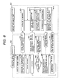
- Fig. 6 is a flowchart illustrating an example of processing according to this embodiment.
- a target wafer is loaded in an electron beam lithography system main body 650 in a step 601.
- this electron beam lithography system main body 650 means the electro-optic system 106 in the embodiment shown in Fig. 1.
- the load of the target wafer means the placement of the target wafer 1 on the target holder 2 in the vacuum chamber 108 by use of the target loader 109.
- a temperature of the loaded target wafer is measured to create initial temperature distribution data 614 of the target wafer.
- the initial temperature distribution data 614 is then supplied to an arithmetic unit 651 for calculating the amount of compensation of beam deflection.
- this beam-deflection compensation amount arithmetic unit 651 is the thermal-deformation calculating computer 103 in the embodiment shown in Fig. 1.
- a temperature of the target wafer at this time can be considered to be the same as that of the target holder 2, the temperature is generally measured by a temperature sensor provided on the target holder 2.
- a storage device for storing temperature distribution of the target wafer is initialized using this data in a step 609. It is to be noted that the steps up to this point can also be omitted if the temperature of the target wafer is kept sufficiently uniform while the target wafer is kept in storage, and also if a temperature of the stage is kept the same as the temperature of the target wafer.
- drawing on the target wafer by an electron beam is started according to a drawing program.
- Drawing beam intensity data and drawing position data 615 at this time are always passed to the target-wafer temperature-distribution storage device 651 where current temperature distribution of the target wafer is always calculated and stored as processing of steps 610 and 611.
- the processing proceeds to a step 606.
- a position 616 to which an electron beam should be applied is obtained from the drawing program, and the position is then passed to the beam-deflection compensation amount arithmetic unit 651.
- the amount of compensation of the beam applying position is calculated according to the position 616. Then, the amount of compensation of beam deflection 617 which has been calculated is returned to the electron beam lithography system main body 650 as compensation data. After that, the beam deflection is compensated in a step 607, and the processing returns to the step 604, the next drawing is performed.
- the processing proceeds from the step 605 to the step 608 where the target wafer is ejected before ending the drawing.
- the compensation data is calculated in real time while monitoring a dose, and an applying position of an electron beam, it is possible to flexibly cope with even a case where an electron-beam applying program is changed on the way. This means that it is possible to cope with even a case where, for example, operation of an electron beam source stops during drawing, causing a part of the drawing to be missed.
- an object of the present invention is to realize a system that is capable of electron beam lithography with a high degree of accuracy regardless of an increase in temperature of a target wafer.
- the object in order to prevent the accuracy of position from being deteriorated by an increase in temperature of the target wafer, which is inevitability caused by an electron beam, the object is achieved by estimating the temperature distribution of the target wafer with a high degree of accuracy without actually measuring the temperature distribution, and then by controlling deflection of the electron beam in response to the obtained temperature distribution.
- an electron beam lithography system capable of obtaining the optimum amount of compensation of an electron-beam applying position in association with a dose and the applying position distribution of an electron beam, and also with the temperature distribution and nonuniform expansion of a target wafer which differ according to electron-beam applying time.
- thermal expansion of the target wafer which is thermally isolated can be estimated with a high degree of accuracy.
- the electron beam lithography can be performed with a high degree of accuracy. Accordingly, the thermal design of a wafer stage is facilitated, which makes it possible to improve the design of the stage with respect to the mechanical accuracy of positioning.
- an electron-beam applying position can be flexibly compensated.
- an electron beam lithography system that applies an electron beam to a target wafer such as a semiconductor wafer, and that thereby draws a pattern circuit, or the like, it is possible to provide an electron beam lithography system and an electron beam lithography method which minimize the effect on drawing discrepancy caused by thermal expansion of the target wafer so as to achieve drawing with a high degree of accuracy.
Landscapes
- Chemical & Material Sciences (AREA)
- Engineering & Computer Science (AREA)
- Nanotechnology (AREA)
- Analytical Chemistry (AREA)
- Physics & Mathematics (AREA)
- Crystallography & Structural Chemistry (AREA)
- Manufacturing & Machinery (AREA)
- General Physics & Mathematics (AREA)
- Condensed Matter Physics & Semiconductors (AREA)
- Mathematical Physics (AREA)
- Theoretical Computer Science (AREA)
- Electron Beam Exposure (AREA)
- Exposure And Positioning Against Photoresist Photosensitive Materials (AREA)
Applications Claiming Priority (2)
| Application Number | Priority Date | Filing Date | Title |
|---|---|---|---|
| JP2002289879 | 2002-10-02 | ||
| JP2002289879A JP2004128196A (ja) | 2002-10-02 | 2002-10-02 | 電子線描画装置と電子線描画方法 |
Publications (2)
| Publication Number | Publication Date |
|---|---|
| EP1406291A2 true EP1406291A2 (de) | 2004-04-07 |
| EP1406291A3 EP1406291A3 (de) | 2005-11-09 |
Family
ID=31987165
Family Applications (1)
| Application Number | Title | Priority Date | Filing Date |
|---|---|---|---|
| EP03022163A Withdrawn EP1406291A3 (de) | 2002-10-02 | 2003-09-30 | Vorrichtung und Verfahren zur Elektronenstrahllithographie |
Country Status (3)
| Country | Link |
|---|---|
| US (1) | US20040065848A1 (de) |
| EP (1) | EP1406291A3 (de) |
| JP (1) | JP2004128196A (de) |
Cited By (1)
| Publication number | Priority date | Publication date | Assignee | Title |
|---|---|---|---|---|
| US7710539B2 (en) | 2005-10-12 | 2010-05-04 | Asml Netherlands B.V. | Method and arrangement for predicting thermally-induced deformation of a substrate, and a semiconductor device |
Families Citing this family (7)
| Publication number | Priority date | Publication date | Assignee | Title |
|---|---|---|---|---|
| JP2005294754A (ja) * | 2004-04-05 | 2005-10-20 | Toshiba Corp | 電子ビーム描画装置、電子ビーム描画方法、電子ビーム描画プログラム及び直接描画方式を用いた半導体装置の製造方法 |
| JP4557682B2 (ja) * | 2004-11-09 | 2010-10-06 | 株式会社東芝 | 電子ビーム描画装置、偏向アンプ、及び電子ビーム描画方法 |
| JP5202136B2 (ja) | 2008-07-02 | 2013-06-05 | 株式会社日立ハイテクノロジーズ | 荷電粒子線装置 |
| NL2011592A (en) * | 2012-10-31 | 2014-05-06 | Asml Netherlands Bv | Compensation for patterning device deformation. |
| JP6245838B2 (ja) | 2013-04-30 | 2017-12-13 | キヤノン株式会社 | リソグラフィ装置、リソグラフィ方法、および物品の製造方法 |
| US10290528B2 (en) | 2014-06-13 | 2019-05-14 | Intel Corporation | Ebeam align on the fly |
| JP7034825B2 (ja) * | 2018-05-16 | 2022-03-14 | 株式会社ニューフレアテクノロジー | 荷電粒子ビーム描画装置及び荷電粒子ビーム描画方法 |
Family Cites Families (3)
| Publication number | Priority date | Publication date | Assignee | Title |
|---|---|---|---|---|
| US5892237A (en) * | 1996-03-15 | 1999-04-06 | Fujitsu Limited | Charged particle beam exposure method and apparatus |
| US5847959A (en) * | 1997-01-28 | 1998-12-08 | Etec Systems, Inc. | Method and apparatus for run-time correction of proximity effects in pattern generation |
| US6440619B1 (en) * | 2000-05-25 | 2002-08-27 | Board Of Supervisors Of Louisiana State University And Agricultural And Mechanical College | Method of distortion compensation by irradiation of adaptive lithography membrane masks |
-
2002
- 2002-10-02 JP JP2002289879A patent/JP2004128196A/ja active Pending
-
2003
- 2003-09-30 EP EP03022163A patent/EP1406291A3/de not_active Withdrawn
- 2003-10-01 US US10/674,467 patent/US20040065848A1/en not_active Abandoned
Cited By (2)
| Publication number | Priority date | Publication date | Assignee | Title |
|---|---|---|---|---|
| US7710539B2 (en) | 2005-10-12 | 2010-05-04 | Asml Netherlands B.V. | Method and arrangement for predicting thermally-induced deformation of a substrate, and a semiconductor device |
| US7710538B2 (en) | 2005-10-12 | 2010-05-04 | Asml Netherlands B.V. | Method and arrangement for correcting thermally-induced field deformations of a lithographically exposed substrate |
Also Published As
| Publication number | Publication date |
|---|---|
| EP1406291A3 (de) | 2005-11-09 |
| JP2004128196A (ja) | 2004-04-22 |
| US20040065848A1 (en) | 2004-04-08 |
Similar Documents
| Publication | Publication Date | Title |
|---|---|---|
| US8698052B2 (en) | Temperature control method of heat processing plate, computer storage medium, and temperature control apparatus of heat processing plate | |
| US6610968B1 (en) | System and method for controlling movement of a workpiece in a thermal processing system | |
| US7900896B2 (en) | Specimen stage | |
| KR100533783B1 (ko) | 경사진 컬럼을 사용한 포커싱된 입자 빔 시스템 및 그 이용 방법 | |
| Larroche et al. | Maxwell-Bloch modeling of x-ray-laser-signal buildup in single-and double-pass configurations | |
| US20040065848A1 (en) | Electron beam lithography system and method therefor | |
| US9502208B2 (en) | Charged particle beam apparatus, stage controlling method, and stage system | |
| TWI409910B (zh) | 半導體製造方法與裝置 | |
| CA2334388A1 (en) | System and method to correct for distortion caused by bulk heating in a substrate | |
| JP6873218B2 (ja) | ミリ秒アニールシステムにおける基板支持 | |
| US20040107066A1 (en) | Methods and apparatus for deriving thermal flux data for processing a workpiece | |
| KR20110050405A (ko) | 워크피스 파손 방지 방법 및 장치 | |
| JP2024518757A (ja) | ウエハの裏面への注入による局所的応力変調 | |
| JP2006344931A (ja) | パルスイオンビームによる表面改質のための局所エッチングまたは堆積の制御 | |
| US6347535B2 (en) | Heating apparatus and method | |
| JPH0636997A (ja) | 電子線描画装置 | |
| KR102241070B1 (ko) | 하전 입자 빔 묘화 장치 및 하전 입자 빔 묘화 방법 | |
| JP6018789B2 (ja) | 荷電粒子線装置 | |
| US20250224703A1 (en) | Operation apparatus, and distributed method for compensating for spacing between two workpieces | |
| JP3422991B2 (ja) | 荷電粒子描画装置 | |
| CN108885092A (zh) | 用于基板应力和变形测量的计量系统 | |
| US20190244784A1 (en) | Method of processing a surface by means of a particle beam | |
| US9703212B2 (en) | Exposure apparatus | |
| JPH0945605A (ja) | 電子線描画装置 | |
| US11081405B2 (en) | Method for measurement of semiconductor device fabrication tool implement |
Legal Events
| Date | Code | Title | Description |
|---|---|---|---|
| PUAI | Public reference made under article 153(3) epc to a published international application that has entered the european phase |
Free format text: ORIGINAL CODE: 0009012 |
|
| AK | Designated contracting states |
Kind code of ref document: A2 Designated state(s): AT BE BG CH CY CZ DE DK EE ES FI FR GB GR HU IE IT LI LU MC NL PT RO SE SI SK TR |
|
| AX | Request for extension of the european patent |
Extension state: AL LT LV MK |
|
| PUAL | Search report despatched |
Free format text: ORIGINAL CODE: 0009013 |
|
| AK | Designated contracting states |
Kind code of ref document: A3 Designated state(s): AT BE BG CH CY CZ DE DK EE ES FI FR GB GR HU IE IT LI LU MC NL PT RO SE SI SK TR |
|
| AX | Request for extension of the european patent |
Extension state: AL LT LV MK |
|
| AKX | Designation fees paid | ||
| STAA | Information on the status of an ep patent application or granted ep patent |
Free format text: STATUS: THE APPLICATION IS DEEMED TO BE WITHDRAWN |
|
| 18D | Application deemed to be withdrawn |
Effective date: 20060510 |
|
| REG | Reference to a national code |
Ref country code: DE Ref legal event code: 8566 |