EP1401095A1 - Montage amplificateur opérationnel - Google Patents
Montage amplificateur opérationnel Download PDFInfo
- Publication number
- EP1401095A1 EP1401095A1 EP02292307A EP02292307A EP1401095A1 EP 1401095 A1 EP1401095 A1 EP 1401095A1 EP 02292307 A EP02292307 A EP 02292307A EP 02292307 A EP02292307 A EP 02292307A EP 1401095 A1 EP1401095 A1 EP 1401095A1
- Authority
- EP
- European Patent Office
- Prior art keywords
- arrangement
- coupled
- linear
- output terminal
- amplifier
- Prior art date
- Legal status (The legal status is an assumption and is not a legal conclusion. Google has not performed a legal analysis and makes no representation as to the accuracy of the status listed.)
- Withdrawn
Links
Images


Classifications
-
- H—ELECTRICITY
- H03—ELECTRONIC CIRCUITRY
- H03F—AMPLIFIERS
- H03F1/00—Details of amplifiers with only discharge tubes, only semiconductor devices or only unspecified devices as amplifying elements
- H03F1/32—Modifications of amplifiers to reduce non-linear distortion
- H03F1/3211—Modifications of amplifiers to reduce non-linear distortion in differential amplifiers
-
- H—ELECTRICITY
- H03—ELECTRONIC CIRCUITRY
- H03F—AMPLIFIERS
- H03F1/00—Details of amplifiers with only discharge tubes, only semiconductor devices or only unspecified devices as amplifying elements
- H03F1/02—Modifications of amplifiers to raise the efficiency, e.g. gliding Class A stages, use of an auxiliary oscillation
-
- H—ELECTRICITY
- H03—ELECTRONIC CIRCUITRY
- H03F—AMPLIFIERS
- H03F3/00—Amplifiers with only discharge tubes or only semiconductor devices as amplifying elements
- H03F3/20—Power amplifiers, e.g. Class B amplifiers, Class C amplifiers
- H03F3/21—Power amplifiers, e.g. Class B amplifiers, Class C amplifiers with semiconductor devices only
- H03F3/211—Power amplifiers, e.g. Class B amplifiers, Class C amplifiers with semiconductor devices only using a combination of several amplifiers
-
- H—ELECTRICITY
- H03—ELECTRONIC CIRCUITRY
- H03F—AMPLIFIERS
- H03F2200/00—Indexing scheme relating to amplifiers
- H03F2200/432—Two or more amplifiers of different type are coupled in parallel at the input or output, e.g. a class D and a linear amplifier, a class B and a class A amplifier
Definitions
- the present invention relates to an operational amplifier arrangement, and more particularly operational amplifier arrangements which can be used as line drivers in telecommunication line circuits.
- Line driver circuits are already known in the art and comprise the classical class-G-based operational amplifiers such as these for instance described in published European Patent Applications 1 024 592 and 1 024 591.
- Other line driver circuits are based on switching line drivers such as the one described in the published European Patent Application 1 229 641.
- Yet other types of line drivers are based on class C-AB architectures, such as these disclosed in published European Patent application 1 220 442 and 1 220 443.
- Key issues for line drivers in applications such as ADSL, which is the abbreviation of asymmetric digital subscriber line, are the power efficiency, the linearity and the complexity.
- VDSL very high speed digital subscriber line applications
- An object of the present invention is thus to provide an operational amplifier arrangement which is power efficient, linear and simple.
- differential embodiments for driving differential signals to two-wire loads.
- the relationships between corresponding amplifiers, resistors and active back terminating arrangements thereby guarantees further linearity and symmetry of the differential embodiments.
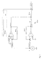
- the operational amplifier arrangement OAA depicted in Fig. 1 includes an input terminal IN, an output terminal OUT, and two pairs of supply terminals (not shown on Fig. 1).
- an input voltage from a source Vin for instance being the signal delivered by the D-A converter in ADSL applications.
- This input terminal is coupled to the respective input terminals of two amplifiers: a non-linear amplifier A2 and a linear amplifier A3.
- a non-linear amplifier may for instance consist of a class-B amplifier as indicated in Fig. 1.
- other types of non-linear amplifiers are possible such as switching mode amplifiers, class C or class D amplifiers. In general a very power efficient amplifier will be chosen for this non-linear amplifier in this operational amplifier arrangement.
- the non-linear amplifier power supply terminals are coupled to one pair of supply terminals of the operational amplifier arrangement, whereas the linear amplifier has power supply terminals which are coupled to the other pair of supply terminals of the operational amplifier arrangement.
- the supply voltage of the linear amplifier is thereby higher in amplitude than the supply voltage of the non-linear amplifier.
- both linear and non-linear amplifiers are operative between the highest supply voltage. Power efficiency of the arrangement is nevertheless improved for the preferred embodiment whereby the non-linear amplifier operates at a lower supply voltage than the linear amplifier.
- the non-linear amplifier A2 has an output terminal OUT A2, and has a first feedback impedance RFA2 coupled between this output terminal OUTA2 and an input terminal IN1A2.
- Another input terminal IN2A2 of this amplifier is coupled to the ground reference in this single-ended embodiment.
- the input voltage may be reduced by means of an input resistor RinA2 coupled between the input terminal IN of the arrangement and the first terminal IN1A2.
- another input resistor RINA3 may be placed in the input path of the linear amplifier A3, thus between the arrangement input terminal IN and a first input terminal IN1A3 of the linear amplifier A3.
- This linear amplifier similarly has a second input terminal IN2A3, coupled to the ground reference.
- the output terminal OUTA3 of the linear amplifier is further coupled via a second feedback impedance RFA3, to the first input terminal IN1A3, and also to the output terminal OUTA2 of the non-linear amplifier, by means of an output series impedance R1.
- OUTA3 is also coupled to the arrangement output terminal OUT, via a terminating impedance Rterm.
- the operational amplifier arrangement OAA further includes an active backterminaton arrangement, which, in the embodiment depicted in Fig. 1 simply consists of a feedforward impedance RFABT, coupled between the arrangement output terminal OUT and the second input terminal IN2A3.
- this active back termination arrangement may consist of an invertor in series with a similar feedforward impedance, both of which are coupled in series between the arrangement output terminal OUT and the first input terminal IN1A3 of the linear amplifier A3.
- the gain which is provided by the non-linear amplifier part between IN and OUT thus including RINA2, A2, RFA2, R1 and Rterm equals the gain which is provided by the linear amplifier part between IN and OUT, including RINA3, A3, RFA3, RjA3, RFABT and RTERM.
- the part of the output impedance of the arrangement, seen from the output terminal with only RTERM, A3, RFA3, RFABT concerned, has to be the same as the part of the output impedance of the arrangement, also seen from the output terminal , but with only RTERM, R1, A2 and RFA2 concerned.
- the philosophy behind both requirements is that the operational amplifier arrangement consists of two equivalent paths in parallel of which the possible distortions caused by the non-linear amplifier are corrected by means of the linear one.
- VoutA3 ( Vin - (Zout/G).lout.G ).A3 whereby G is the gain of the block consisting of amplifier A1, and impedances k.Rterm, and k.Zline, depicted by means of their resistance values, and A3 here depicts the gain of the linear amplifier A3 and its input resistors and feedback resistors.
- Equation (5) thus gives the basis for the synthesis of Zout, which needs to be equal to the load impedance, corresponding to the line impedance Zline, in the case of a line driver.
- This is performed by the Active back termination arrangement, which, in a very simple embodiment can merely consist of one resistor couplejd between the arrangement output terminal and an input terminal of the linear amplifier, as was already described for the embodiment of Fig. 1.
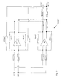
- FIG. 2 a differential embodiment OAA', including two halfs, each of which is similar to the embodiment depicted in Fig. 1, is shown.
- the first half coupled to input terminal IN, includes a non-linear amplifier A2, possibly operating at a lower supply voltage than a linear amplifier A3.
- the linear amplifier has input resistors RinA3, RjA3, and a feedback resistor RFA3, whereas the non-linear amplifier A2 of the first branch includes has input resistor RinA2, feedback resistor RFA2.
- the output terminal OUTA2 of the non-linear amplifier A2 is coupled via a series impedance R1 to the output terminal OUTA3 of the linear amplifier A3.
- a terminating impedance Rterm is coupled between OUTA3 and a first arrangement output terminal OUT, whereby this first arrangement output terminal is coupled via an active backtermination arrangement, in the embodiment depicted in Fig. 2 simply consisting of a resistor RFABT, is coupled to an input terminal IN2A3 of the linear amplifier A3.
- Linear amplifier A3' has input resistors RinA3' and RjA3', and a feedback resistance RFA3'.
- Non-linear amplifier A2' has input resistor RinA2', and feedback resistor RFA2'.
- the single output of A2', denoted OUTA2' is coupled via a second series impedance R1' to the output terminal OUTA3' of A3'.
- a second terminating impedance Rterm' is coupled between OUTA3' and the second arrangement output terminal OUT', whereas this second arrangement output terminal is coupled to an input terminal of the linear amplifier A3' via a second active backtermination arrangment ABT', in the embodiment depicted in Fig. 2 simply consisting of an impedance RFABT' coupled between OUT' and IN2A3'.
- A2 and A2' are chosen as similar amplifiers, as well as A3 and A3' whereby also the respective input and feedback impedances of the corresponding amplifiers have substantially equal values.
- Series impedances R1 and R1' are similar as well as, terminating impedances Rterm and Rterm' and active backterminating impedances RFABT and RFABT'.
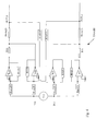
- the differential operational amplifier arrangement OAA" depicted in Fig. 3 also includes two arrangement input terminals IN1" and IN2", as well as two arrangement output terminals OUT1" and OUT2", but only includes one amplifier of each type, namely a linear amplifier A3", again operating between the highest supply voltage rails, and a non-linear amplifier A2" possibly operating at a lower supply voltage.
- Both linear and non-linear amplifiers have two input terminals and two output terminals, respectively coupled to the two arrangement input terminals and the two arrangement output terminals as can be observed from Fig. 3.
- the arrangement input terminals are thereby coupled to the linear amplifier input terminals via two respective input resistors, both denoted RinA3" which are also substantially equal because of stability.
- two substantially equal input resistors, both denoted RinA2" are coupled between arrangement input terminals and respective non-linear amplifier input terminals.
- A3" has two similar feedback impedances, both denoted RFA3". The same holds for A2" having also two similar feedback impedances both denoted RFA2" because they have substantially equal values.
- Output terminals of A2" are coupled to corresponding output terminals of A3" via respective series impedances, both denoted R1" because they are similar. With corresponding output terminals is meant that both output terminals of these amplifiers are delivering the same sign of signal at a moment in time. In other words, the positive output terminal of A2" is coupled to the positive output terminal of A3" and vice versa.
- the output terminals of A3" are further coupled to the corresponding arrangement output terminals OUT1" and OUT2" via respective terminating impedances , both denoted Rterm" since these are also similar for symmetry reasons.
- these arrangement output terminals are coupled to the non-corresponding input terminals of the linear amplifiers via respective active back terminating arrangements, in the embodiment depicted in Fig. 3 merely consisting of resistors.
- these active back terminating arrangements may again consist of a series coupling of a resistor and an invertor, in which case arrangement output terminals are connected via this type of active back terminating arrangements, to the corresponding input terminals of the linear amplifier A3".
- OAA10 which shows a lot of resemblance with the one depicted in Fig. 2, is shown in Fig. 4. It again consists of two halfs : a first one consisting of a first parallel branch including non-linear amplifier A20, series impedance R10 and terminating impedance Rterm 10, and a second parallel branch with linear amplifier A30 and the same terminating impedance Rterm 10. Both amplifiers may further have feedback such as depicted by RFA20 and RFA30 respectively, as well as input resistance respectively depicted by RinA20 and RinA30.
- the second half of the embodiment of Fig. 4 again consists of two parallel branches : a first one via linear amplifier A31 and a second terminating impedance denoted Rterm11, and a second one via non-linear amplifier A21, series impedance R11 and terminating impedance Rterm11.
- the respective amplifiers may have respective input resistors , respectively denoted RinA31 and RinA21, as well as feedback, respectively denoted by RFA31 and RFA21.
- active back terminating resistor RFABT10 is coupled between an arrangement output terminal belonging to one upper half of the arrangement, and an input terminal of the linear amplifier belonging to the lower half of the arrangement.
- active back terminating resistor RFABT11 is coupled between an arrangement output terminal of the lower half to an input terminal of the linear amplifier of the upper half.
- FIG. 5 The embodiment depicted in Fig. 5 is basically similar to the one depicted in Fig. 4, except for the addition of another pair of active backterminating arrangements, in the embodiment of Fig. 5 consisting of resistors RFABT100 and RFABT101 respectively.
- This second pair of active back terminating resistors is thereby cross-coupled between an output terminal of a linear amplifier of one half of the arrangement, to an input terminal of a non-linear amplifier of the other half of the arrangement.
- output terminal of A31' is coupled to input terminal of A20' via active back terminating resistor RFABT101 while output terminal of A30' is coupled to input terminal of A21' via active back terminating resistor RFABT100.
- the second active back termination is realised by means of cross-coupling.
- the output of the linear amplifier A31 can also be coupled, via a single resistor, to the "+" input of A21', or via a series connection of a single resistor and an invertor to the "-" input of A21' for the embodiment depicted in Fig. 5. Similar considerations hold for the active back termination in the upper half of the scheme.
Landscapes
- Engineering & Computer Science (AREA)
- Power Engineering (AREA)
- Physics & Mathematics (AREA)
- Nonlinear Science (AREA)
- Amplifiers (AREA)
Priority Applications (2)
| Application Number | Priority Date | Filing Date | Title |
|---|---|---|---|
| EP02292307A EP1401095A1 (fr) | 2002-09-20 | 2002-09-20 | Montage amplificateur opérationnel |
| US10/664,856 US7042284B2 (en) | 2002-09-20 | 2003-09-22 | Operational amplifier arrangement |
Applications Claiming Priority (1)
| Application Number | Priority Date | Filing Date | Title |
|---|---|---|---|
| EP02292307A EP1401095A1 (fr) | 2002-09-20 | 2002-09-20 | Montage amplificateur opérationnel |
Publications (1)
| Publication Number | Publication Date |
|---|---|
| EP1401095A1 true EP1401095A1 (fr) | 2004-03-24 |
Family
ID=31896991
Family Applications (1)
| Application Number | Title | Priority Date | Filing Date |
|---|---|---|---|
| EP02292307A Withdrawn EP1401095A1 (fr) | 2002-09-20 | 2002-09-20 | Montage amplificateur opérationnel |
Country Status (2)
| Country | Link |
|---|---|
| US (1) | US7042284B2 (fr) |
| EP (1) | EP1401095A1 (fr) |
Cited By (2)
| Publication number | Priority date | Publication date | Assignee | Title |
|---|---|---|---|---|
| EP1615340A1 (fr) * | 2004-07-09 | 2006-01-11 | Alcatel | Procédé de réalisation d'un circuit électronique avec fonction de transfer desirée et arrangement obtenu selon ce procédé |
| EP2341616A1 (fr) * | 2009-12-23 | 2011-07-06 | STMicroelectronics Design and Application S.R.O. | Amplificateur de commande de charge capacitive |
Families Citing this family (14)
| Publication number | Priority date | Publication date | Assignee | Title |
|---|---|---|---|---|
| DE10300011B4 (de) * | 2003-01-02 | 2004-09-16 | Infineon Technologies Ag | Subtrahiererschaltung und Leistungsdetektoranordnung mit der Subtrahiererschaltung |
| US20070069811A1 (en) * | 2005-09-21 | 2007-03-29 | Schley-May James T | Line drivers with extended linearity |
| US20070236295A1 (en) * | 2006-03-21 | 2007-10-11 | Leadis Technology, Inc. | FM Power Amplifier With Antenna Power Control |
| US7408414B2 (en) * | 2006-03-21 | 2008-08-05 | Leadis Technology, Inc. | Distributed class G type amplifier switching method |
| US7498880B2 (en) * | 2006-03-21 | 2009-03-03 | Leadis Technology, Inc. | Class L amplifier |
| US8081777B2 (en) | 2006-03-21 | 2011-12-20 | Fairchild Semiconductor Corporation | Volume-based adaptive biasing |
| US8081785B2 (en) * | 2006-03-21 | 2011-12-20 | Fairchild Semiconductor Corporation | High efficiency converter providing switching amplifier bias |
| US7522433B2 (en) * | 2006-03-21 | 2009-04-21 | Fairchild Semiconductor Corporation | Efficient voltage rail generation |
| US20070285176A1 (en) * | 2006-03-21 | 2007-12-13 | Leadis Technology, Inc. | Phase-Slipping Phase-Locked Loop |
| US8179372B1 (en) | 2007-10-01 | 2012-05-15 | Integrated Device Technology, Inc. | Electronic display with array context-sensitive search (ACS) technology |
| US7733178B1 (en) | 2007-10-24 | 2010-06-08 | Fairchild Semiconductor Corporation | High efficiency audio amplifier |
| US7750732B1 (en) | 2007-12-04 | 2010-07-06 | Fairchild Semiconductor Corporation | Adaptive rail amplifier (ARA) technology |
| TWI346446B (en) * | 2008-04-21 | 2011-08-01 | Advanced Analog Technology Inc | Multi-input operational amplifier and method for reducing input offset thereof |
| US10732931B2 (en) * | 2018-11-28 | 2020-08-04 | International Business Machines Corporation | Negative operand compatible charge-scaling subtractor circuit |
Citations (4)
| Publication number | Priority date | Publication date | Assignee | Title |
|---|---|---|---|---|
| US5438684A (en) * | 1992-03-13 | 1995-08-01 | Motorola, Inc. | Radio frequency signal power amplifier combining network |
| US6028485A (en) * | 1998-08-03 | 2000-02-22 | Motorola, Inc. | Power amplification apparatus and method therefor |
| DE10054540A1 (de) * | 2000-11-03 | 2002-06-06 | Xignal Technologies Ag | Leistungseffiziente Verstärkerschaltung und Verfahren zur leistungseffizienten Verstärkung eines Signals |
| EP1220442A1 (fr) * | 2000-12-28 | 2002-07-03 | Alcatel | Circuit d'attaque xDSL de classe c-ab avec boucle de retroaction |
Family Cites Families (6)
| Publication number | Priority date | Publication date | Assignee | Title |
|---|---|---|---|---|
| US5374966A (en) * | 1993-04-15 | 1994-12-20 | Westinghouse Electric Corporation | Low noise impedance-matched video amplifier |
| DE69934966T2 (de) | 1999-01-28 | 2007-11-08 | Alcatel Lucent | Leistungsverstärkervorrichtung |
| EP1024592B1 (fr) | 1999-01-29 | 2007-02-21 | Alcatel | Dispositif amplificateur de puissance |
| US6300828B1 (en) * | 2000-01-20 | 2001-10-09 | Next Level Communications | Switchless high efficiency amplifier |
| ATE513360T1 (de) | 2000-12-28 | 2011-07-15 | Alcatel Lucent | Xdsl klasse c-ab treiber |
| EP1229641B1 (fr) | 2001-02-01 | 2013-11-06 | Alcatel Lucent | Amplificateur de puissance auto-oscillant |
-
2002
- 2002-09-20 EP EP02292307A patent/EP1401095A1/fr not_active Withdrawn
-
2003
- 2003-09-22 US US10/664,856 patent/US7042284B2/en not_active Expired - Fee Related
Patent Citations (4)
| Publication number | Priority date | Publication date | Assignee | Title |
|---|---|---|---|---|
| US5438684A (en) * | 1992-03-13 | 1995-08-01 | Motorola, Inc. | Radio frequency signal power amplifier combining network |
| US6028485A (en) * | 1998-08-03 | 2000-02-22 | Motorola, Inc. | Power amplification apparatus and method therefor |
| DE10054540A1 (de) * | 2000-11-03 | 2002-06-06 | Xignal Technologies Ag | Leistungseffiziente Verstärkerschaltung und Verfahren zur leistungseffizienten Verstärkung eines Signals |
| EP1220442A1 (fr) * | 2000-12-28 | 2002-07-03 | Alcatel | Circuit d'attaque xDSL de classe c-ab avec boucle de retroaction |
Non-Patent Citations (1)
| Title |
|---|
| NAM-SUNG JUNG ET AL: "A new high-efficiency and super-fidelity analog audio amplifier with the aid of digital switching amplifier: class K amplifier", POWER ELECTRONICS SPECIALISTS CONFERENCE, 1998. PESC 98 RECORD. 29TH A NNUAL IEEE FUKUOKA, JAPAN 17-22 MAY 1998, NEW YORK, NY, USA,IEEE, US, vol. 1, 17 May 1998 (1998-05-17), pages 457 - 463, XP010294931, ISBN: 978-0-7803-4489-1, DOI: 10.1109/PESC.1998.701938 * |
Cited By (2)
| Publication number | Priority date | Publication date | Assignee | Title |
|---|---|---|---|---|
| EP1615340A1 (fr) * | 2004-07-09 | 2006-01-11 | Alcatel | Procédé de réalisation d'un circuit électronique avec fonction de transfer desirée et arrangement obtenu selon ce procédé |
| EP2341616A1 (fr) * | 2009-12-23 | 2011-07-06 | STMicroelectronics Design and Application S.R.O. | Amplificateur de commande de charge capacitive |
Also Published As
| Publication number | Publication date |
|---|---|
| US7042284B2 (en) | 2006-05-09 |
| US20040056713A1 (en) | 2004-03-25 |
Similar Documents
| Publication | Publication Date | Title |
|---|---|---|
| EP1401095A1 (fr) | Montage amplificateur opérationnel | |
| JP3502264B2 (ja) | 受信装置 | |
| JP4071395B2 (ja) | 利得可変増幅器 | |
| JP2007538449A (ja) | 自動ゲイン補正を有する増幅器回路 | |
| US7132860B2 (en) | Differential-mode current feedback amplifiers | |
| US6351185B1 (en) | Increased output swing line drivers for operation at supply voltages that exceed the breakdown voltage of the integrated circuit technology | |
| US6507223B2 (en) | Differential line driver having adjustable common mode operation | |
| JP2013542635A (ja) | ファントムモード伝送のための結合構成 | |
| US20060006941A1 (en) | Class D-amplifier | |
| US6570430B1 (en) | Non-linear distortion generator for both second and third order distortion | |
| WO2006028288A1 (fr) | Circuit de filtre d’egalisation | |
| US6580760B1 (en) | Line drive architecture with programmable gain and drive | |
| US6538510B1 (en) | High efficiency, current sink only line driver | |
| US6509789B1 (en) | Circuit for reducing second and third order intermodulation distortion for a broadband RF amplifier | |
| US6580286B1 (en) | Method and apparatus for active line termination | |
| WO2003007472A1 (fr) | Amplificateur a multiples etages a correction d'erreur locale | |
| US9860086B1 (en) | Equalizer circuit and optical module | |
| US6630866B2 (en) | High beta output stage for high speed operational amplifier | |
| US6794941B2 (en) | Gain-controlled amplifier with fixed minimum gain | |
| KR100528658B1 (ko) | 하이브리드 증폭기 | |
| NL8702378A (nl) | Brede-band gelijkspanningsniveau verschuivingsketen met terugkoppeling. | |
| US6794943B2 (en) | Ultra linear high speed operational amplifier output stage | |
| US7116132B2 (en) | Current feedback amplifiers with separate common-mode and differential-mode inputs | |
| US7132859B2 (en) | Common-mode current feedback amplifiers | |
| US6647116B1 (en) | Current sensing circuit and ADSL interface circuit |
Legal Events
| Date | Code | Title | Description |
|---|---|---|---|
| PUAI | Public reference made under article 153(3) epc to a published international application that has entered the european phase |
Free format text: ORIGINAL CODE: 0009012 |
|
| AK | Designated contracting states |
Kind code of ref document: A1 Designated state(s): AT BE BG CH CY CZ DE DK EE ES FI FR GB GR IE IT LI LU MC NL PT SE SK TR |
|
| AX | Request for extension of the european patent |
Extension state: AL LT LV MK RO SI |
|
| 17P | Request for examination filed |
Effective date: 20040924 |
|
| AKX | Designation fees paid |
Designated state(s): AT BE BG CH CY CZ DE DK EE ES FI FR GB GR IE IT LI LU MC NL PT SE SK TR |
|
| RAP1 | Party data changed (applicant data changed or rights of an application transferred) |
Owner name: ALCATEL LUCENT |
|
| 17Q | First examination report despatched |
Effective date: 20070525 |
|
| RAP1 | Party data changed (applicant data changed or rights of an application transferred) |
Owner name: ALCATEL LUCENT |
|
| STAA | Information on the status of an ep patent application or granted ep patent |
Free format text: STATUS: THE APPLICATION IS DEEMED TO BE WITHDRAWN |
|
| 111Z | Information provided on other rights and legal means of execution |
Free format text: AT BE BG CH CY CZ DE DK EE ES FI FR GB GR IE IT LI LU MC NL PT SE SK TR Effective date: 20130410 |
|
| 18D | Application deemed to be withdrawn |
Effective date: 20130410 |