EP1401012A2 - Method of forming organic spacers and using them to form semiconductor device features - Google Patents
Method of forming organic spacers and using them to form semiconductor device features Download PDFInfo
- Publication number
- EP1401012A2 EP1401012A2 EP03021102A EP03021102A EP1401012A2 EP 1401012 A2 EP1401012 A2 EP 1401012A2 EP 03021102 A EP03021102 A EP 03021102A EP 03021102 A EP03021102 A EP 03021102A EP 1401012 A2 EP1401012 A2 EP 1401012A2
- Authority
- EP
- European Patent Office
- Prior art keywords
- organic
- forming
- spacers
- areas
- source
- Prior art date
- Legal status (The legal status is an assumption and is not a legal conclusion. Google has not performed a legal analysis and makes no representation as to the accuracy of the status listed.)
- Withdrawn
Links
Images


Classifications
-
- H—ELECTRICITY
- H10—SEMICONDUCTOR DEVICES; ELECTRIC SOLID-STATE DEVICES NOT OTHERWISE PROVIDED FOR
- H10D—INORGANIC ELECTRIC SEMICONDUCTOR DEVICES
- H10D64/00—Electrodes of devices having potential barriers
- H10D64/01—Manufacture or treatment
- H10D64/018—Spacers formed inside holes at the prospective gate locations, e.g. holes left by removing dummy gates
-
- H—ELECTRICITY
- H10—SEMICONDUCTOR DEVICES; ELECTRIC SOLID-STATE DEVICES NOT OTHERWISE PROVIDED FOR
- H10D—INORGANIC ELECTRIC SEMICONDUCTOR DEVICES
- H10D30/00—Field-effect transistors [FET]
- H10D30/01—Manufacture or treatment
- H10D30/021—Manufacture or treatment of FETs having insulated gates [IGFET]
- H10D30/0223—Manufacture or treatment of FETs having insulated gates [IGFET] having source and drain regions or source and drain extensions self-aligned to sides of the gate
- H10D30/0227—Manufacture or treatment of FETs having insulated gates [IGFET] having source and drain regions or source and drain extensions self-aligned to sides of the gate having both lightly-doped source and drain extensions and source and drain regions self-aligned to the sides of the gate, e.g. lightly-doped drain [LDD] MOSFET or double-diffused drain [DDD] MOSFET
-
- H10D64/01326—
-
- H—ELECTRICITY
- H10—SEMICONDUCTOR DEVICES; ELECTRIC SOLID-STATE DEVICES NOT OTHERWISE PROVIDED FOR
- H10D—INORGANIC ELECTRIC SEMICONDUCTOR DEVICES
- H10D64/00—Electrodes of devices having potential barriers
- H10D64/01—Manufacture or treatment
- H10D64/021—Manufacture or treatment using multiple gate spacer layers, e.g. bilayered sidewall spacers
-
- H10P50/268—
-
- H10P50/283—
-
- H10P50/287—
-
- H10P50/73—
-
- H10P76/405—
-
- H10P76/4085—
-
- H10P76/4088—
-
- H10W20/089—
Definitions
- the present invention relates to a method of forming spacers suitable for forming larger S/D (Source/Drain) contact areas and LDD (lightly doped drain) / extension areas and graded junctions for semiconductor devices. More specifically, one embodiment of the invention relates to a method of forming disposable organic spacers using an N 2 plasma etch. Another embodiment of the invention is to use organic spacers as a method of forming semiconductor device features such as larger Source/Drain contact areas with a graded junction or Source/Drain and LDD/extension areas and graded junctions with a single implant step.
- Formation of organic spacers typically occurs while anisotropic carrying out an etching of polysilicon through openings in a patterned photoresist mask with some formulation which includes one or more of C (carbon), H (hydrogen) and F (fluoride), i.e., C x H y F z .
- Suitable formulation may include trifluoromethane (CHF 3 ) or carbon tetrafluoride (CH 2 F 2 ), etc.
- U.S. Patent 5,861,343 issued to Horng-Haei Tseng on January 19, 1999 also discusses a method of forming a self contact hole on a semiconductor substrate by using a patterned photoresist over a polysilicon layer.
- the polysilicon is then etched with an RIE process using a reactant gas such as CH 2 F 3 , CF 4 , C 2 F 6 , HB r or CH 2 to produce the polymer sidewall spacers.
- the polymer sidewall spacers are then used as a mask to form an opening in the polysilicon layer of a reduce size.
- U.S. Patent 5,866,448 issued to Yelehanka R. Pradeepk et al. on February 2, 1999 describes a method for fabricating an LDD area (lightly doped drain) for self aligned polysilicon gate MOSFET's.
- LDD area lightly doped drain
- a polymer layer is formed along the sidewall of the gate during the patterning process of the gate electrode. This layer is then used to mask the S/D (Source/Drain) ion implantation and, according to the patent, provides improved thickness control as well as an improved sequence of process steps since this requirement for a spacer oxide layer is eliminated.
- One embodiment of this invention is a method of forming organic spacers.
- the method comprises providing a patterned semiconductor structure which is then conformally coated with an organic material such as, for example only, an antireflective coating.
- the patterned semiconductor structure coated with the organic material is then anisotropically etched with N 2 plasma or "N 2 containing plasma".
- N 2 containing plasma as used herein is defined as N 2 , which also includes a carrier gas such as, for example, Argon or Helium.
- the step of providing the patterned semiconductor structure is followed by conformally coating the patterned structure with organic material.
- the anisotropic etching step with N 2 plasma of this coated structure forms organic spacers on the sidewall of the etched aperture in the coated area so that further etching through the patterned semiconductor structure results in a opening with reduced size.
- This reduced diameter hole or aperture may then be filled with conductive material.
- the invention provides for manufacturing of semiconductor devices with a larger S/D contact area and/or an LDD/extension area, which may include graded junctions with a single implant step.
- the method of this embodiment of the invention comprises the steps of forming a gate dielectric such as a gate oxide and conductive gate structures. And organic spacers are formed on the sidewall of the conductive gate member.
- the organic spacers can be formed by the method of this invention or any other known method although the method of this invention is believed to be especially effective.
- These organic sidewall spacers are then used as a mask to form S/D regions, and LDD/extension areas, which may include graded junctions. These features may be formed in a single implant step.
- the organic spacer is stripped and a thinner normal permanent spacer may be formed to provide for larger S/D contact area.
- a thinner normal permanent spacer may be formed to provide for larger S/D contact area.
- Still another embodiment of forming larger S/D contact areas, which may include graded junctions comprises the steps of forming a gate dielectric such as a gate oxide and conductive gate structures. Thin permanent spacers are then formed over the conductive gate structures. Organic spacers are then formed over the thin permanent spacer by the method of this invention or any other known method,. An implanted is performed to form the S/D regions and may include graded junctions. The organic spacers are then stripped to provide larger S/D contact areas.
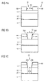
- Figures 1A, 1B, and 1C illustrate a prior art process for forming polymer spacers on a semiconductor device
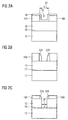
- Figures 2A, 2B, and 2C illustrate a process of the present invention for forming organic spacers on a semiconductor device with N 2 plasma;
- FIG. 3 is a copy of an actual Scanning Electron Microscope (SEM) photograph of organic spacers formed according to the method of the present invention
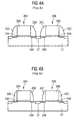
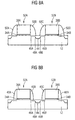
- Figures 4A and 4B illustrate a prior art method of using polysilicon or dielectric-based disposal spacers for forming larger Source/Drain contact areas
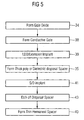
- Figure 5 is a process flow diagram for forming the structures shown in Figures 4A and 4B;
- Figures 6A and 6B illustrate an embodiment of the present invention using an organic disposal spacer for forming larger Source/Drain contact areas and graded junctions;
- Figure 7 is a process flow diagram for forming the structures shown in Figures 6A and 6B;
- Figures 8A and 8B illustrate another embodiment of the present invention of using organic spacers for forming larger Source/Drain contact areas, LDD/extension areas, and graded junctions in one implant step;
- Figure 9 is a process flow diagram for forming the structures shown in Figures 8A and 8B.
- Certain anisotropic etching processing leaves a layer of polymer material on sidewall surfaces around the area subjected to the etching process.
- the formation of such polymer layers may have originally been an undesirable result, the formation of such layers can be used to obtain or form specific features on a semiconductor device. More specifically, the formation of these polymer layers (or spacers) on sidewalls allows etching of vias or openings which are substantially smaller in cross-section than can otherwise be achieved.
- U.S. Patent 5,719,089; 5,861,343 and 6,103,588 discussed above provide examples of forming smaller openings or vias. Further, as described in U.S. Patent 5,866,448 such polymer layers can also be used as a mask during ion implantation to aid in the formation of Source/Drain regions in a semiconductor device.
- an insulating or dielectric layer 10 covers a substrate 12 such as a silicon wafer.
- the dielectric layer 10 may be any suitable oxide such as a SiO 2 , a PMD dielectric (pre-metal dielectric) or other low flow temperature doped oxide such as boronphosilicate glass (BPSG).
- a polysilicon or silicon nitride layer 14 is then deposited over the dielectric layer 10.
- a layer of photoresist such as shown at 16 is then patterned to define areas of 16A and 16B and opening 18.
- the size of the opening 18 has a dimension "D" indicated by the double-headed arrow 22.
- the dimension "D" as an example, may represent the minimum practical dimension that can be obtained with available photoresist and lithographic techniques. When the device dimensions are reduced, device performance increases and manufacturing costs go down. A competitive advantage is achieved by forming device feature sizes smaller than is now possible by existing lithographic techniques.
- the polymer spacers 24A and 24B now act as a mask such that continued etching of the dielectric layer 10 results in a via or opening 26 through the dielectric layer 10 having a substantially reduced cross-section dimension "d" as indicated by the reference numeral 28 in Figure 1C.
- the patterned layer of photoresist 16 along with the poly or nitride layer 14 is then stripped from the dielectric layer 10.
- the via 26 can subsequently be filled with a conductive material to provide a conductive path to the semiconductor area 20 according to methods well known to those skilled in the art.
- FIG. 2A, 2B and 2C there is illustrated the process for forming an organic spacer according to the present invention, which, in the illustrated example, is used to reduce the size of a via or opening as discussed above.
- organic spacers can also be used for forming other features of semiconductor devices as will be discussed later.
- a layer 10 of dielectric material covers a semiconductor substrate such as a silicon wafer 12.
- a patterned layer of photoresist is then formed over the dielectric layer 10 in the same manner as discussed above. It should be noted, however, that unlike the prior art process discussed with respect to Figures 1A, 1B and 1C, a nitride or poly layer is not required.
- a conformal coating 30 of organic material such as, for example, an anti-reflecting coating material is then applied over the patterned layer of photoresist.
- the anti-reflecting coating material AR3 available from the Shipley Company in the state of Massachusetts, has been found effective with the present invention. Also, assuming again that it is desired to provide a conductive path from the top of the dielectric layer 10 to a contact area 20 on the substrate or wafer 12, a via or opening must be provided through the dielectric to contact area 20.
- the patterned semiconductor structure with the organic coating is then subjected to an anisotropic plasma etch in a plasma etcher.
- the plasma etch is comprised only of N 2 plasma or "N 2 containing plasma", such as, for example, N 2 /Ar (argon) plasma or N 2 /He (helium) plasma.
- the "lateral" etch rate for organic material using an N 2 plasma is negligible and limited to around 2 nm/min for all plasma power levels as indicated by Table 1 below. This negligible lateral etch is caused by neutral radicals in N 2 plasma. Table 1 illustrates that neutral radicals in remote N 2 plasma has a negligible etch rate for organic material. Isotropic (lateral) Etch Rate with a remote N 2 Plasma Plasma Power (W) Etch Rate (nm/min) 500 2.3 700 2.1 900 1.8
- the "vertical" etch rate increases significantly with ion enhancement when the etching bias is varied in a normal plasma etcher.
- Table 2 below it is seen from lines 1 and 2 of the table that the etch rate for organic material is increased significantly.
- a self bias exists on the wafer in a normal plasma system when the wafer is directly exposed to plasma. Therefore, even at an RF bias of 0 watt, the etch rate is over 20 times of that in a remote N 2 plasma.
- the RF bias is increased to 500 watts, an increase of almost an additional 10-fold occurs.
- N 2 containing plasma a similar etch rate is also observed as shown in Table 2.
- Tables 1, and 2 show that the etch rate for organic material in the lateral direction in N 2 plasma and "N 2 containing plasma" is almost negligible, and the etch rate in vertical direction is greatly enhanced by bias power of plasma.
- the etch rate for organic material in vertical direction is more than 100 fold faster than that in lateral direction with a bias power of 300W.
- N 2 plasma or N 2 containing plasma is a very effective an-isotropic etchant for organic material.
- anisotropic N 2 plasma etching of the organic coating 30 results in organic spacers 32A and 32B forming on the sidewalls of the patterned photoresist layer 12.
- formed organic spacer 32A and 32 B act as a mask such as continued an-isotropic dielectric etch of layer 10 results in an opening or via having a reduced size "d" to the contact area 20, as shown in Figure 2C.
- a conductive material can now be used to fill the small diameter via to provide a path from area 20 through dielectric layer 10.
- the organic spacer formed by the method disclosed in this invention can also be used to form other device structures, such as larger S/D contact area and graded junction as will be discussed below.
- organic spacers may be used to form enlarged Source/Drain (S/D) contact areas, LDD (lightly doped drain)/extension areas with or without graded junctions. Further, these features may be formed with a single implant step.
- FIG. 4A there is shown a prior art method of using disposable spacers to obtain larger S/D contact areas.
- a gate dielectric layer such as a gate oxide is deposited over a semiconductor substrate such as a silicon wafer 12.
- a conductive material 38 such as polysilicon, is then deposited over the gate dielectric.
- the conductive gate stack is then patterned and etched to define gate structure 38A, 38B.
- An ion implant is performed to form LDD/extension area 39A and 39B.
- thick disposable spacers 35A, 35B, 35C and 35D made of such materials as polysilicon, silicon oxide or silicon nitride are then formed on the sidewalls of the conductive gates.
- the S/D junction 37 is then formed by ion implantation according to methods known to those skilled in the art, as shown in Figure 4A.
- the thick disposable spacers 35A-35D are then removed and smaller permanent spacers 40A, 40B, 40C and 40D are formed to provide larger S/D contact areas, as shown in Figure 4B. It should be noted that this process will not produce graded junctions. It should also be appreciated that the removal of the disposable spacers 35A-35D typically requires a process such as, for example, a dry etch that is damaging to the underlying semiconductor structure such as the gate oxide and/or S/D junctions.
- FIG. 5 A flow diagram for forming the prior art structures illustrated in Figures 4A and 4B is shown in prior art Figure 5.
- a gate dielectric such as oxide is formed over the substrate 12 as indicated by step 34.
- Conductive gates 38A and 38B are formed over the gate oxide as shown at step 38.
- the LDD/extensions 39A and 39B are then implanted into the substrate 12 as indicated at step 39.
- the thick poly or dielectric disposable spacers 35A, 35B, 35C and 35D are then formed on the sidewalls of the conductive gate material 38A and 38B as indicated at step 35.
- Implantation of the S/D 37 is then carried out as indicated at step 41.
- the S/D implant step 41 we have the structure as illustrated by Figure 4A.
- step 41 disposable spacers 35A, 35B, 35C and 35D are then removed such as by etching as indicated at step 43.
- the thin permanent spacers 40A, 40B, 40C and 40D are then formed as shown at step 40 and provide larger S/D contact areas.
- Figure 4B represents this structure.
- step 40 may be followed by the formation of silicide.
- FIGS. 6A and 6B there are illustrated process steps of another embodiment of the invention of using organic spacers as a mask for implanting the S/D areas with graded junctions.
- a gate dielectric layer such as oxide is deposited over a semiconductor substrate such as a silicon wafer 12.
- a conductive material 38 such as polysilicon, is then deposited over the gate dielectric.
- the conductive gate stack is then patterned and etched to define gate structures 38A, 38B.
- An ion implant is performed to form the LDD/extension areas 46A and 46B.
- Methods of forming of the gate oxide and the conductive gates 38A and 38B are well-known in the semiconductor art and will not be discussed further.
- thinner permanent spacers such as silicon oxide or silicon nitride spacers 40A, 40B, 40C and 40D are formed on the sidewalls of the conductive gate, also according to methods well-known in the prior art.
- Disposable organic spacers 42A, 42B, 42C and 42D are then formed in a manner similar to that discussed above with respect to Figures 2A, 2B and 2C or by any other suitable process.
- the organic spacers 42A-42D may be formed according to any suitable process, the process discussed with respect to Figures 2A and 2B is believed to be especially effective.
- Various and different well-known implantation processes for forming the S/D junction 44 may be used during or after the formation of the organic spacers.
- the organic spacers act as a mask to block or partially block the S/D implant.
- the graded junctions 48A and 48B may be formed by implanting ions when the organic spacers 42A - 42D have a common conductive gate thickness of 100nm-300nm since the organic spacers only partially block the S/D implant.
- the organic spacers 42A, 42B, 42C and 42D are typically removed to provide larger S/D contact areas. as shown in Figure 6B.
- FIG. 7 there is shown a flow diagram for forming the structures of the present invention as shown in Figures 6A and 6B. As shown, steps 34, 38 and 39 of Figure 7 are the same as in Figure 5. However, after implantation of the LDD/extensions 46A and 46B, the next step of the inventive process of this invention is forming thin dielectric permanent spacers 40A, 40B, 40C and 40D as shown at step 40. Organic spacers 42A, 42B, 42C and 42D are then formed on the permanent spacers as indicated at step 42. Formation of the S/D 44 with graded junctions 48A and 48B is then accomplished by ion implanting as indicated at step 46. Completion of the ion implanting step 46 results in the structure illustrated in Figure 6A. Organic spacers 42A, 42B, 42C and 42D are then stripped as shown at step 48 and as illustrated in Figure 4B. This provides for larger S/D contact areas.
- Figures 8A and 8B illustrate the process of using the N 2 plasma etched according to still another embodiment of this invention to use disposable organic spacers to form S/D areas and LDD/extension areas with graded junctions, or alternately, to save an LDD/extension implantation step.
- a patterned semiconductor structure which includes areas of gate oxide 34A and 34B as part of the conductive gate stacks 52A and 52B is fabricated in a manner as discussed above with respect to the prior art.
- the disposable organic spacers 50A, 50B, 50C and 50D are then formed in a manner similar to that discussed above with respect to Figures 2A, 2B and 2C or by any other suitable process.
- the organic spacers 50A-50D may be formed according to any suitable process, the process discussed with respect to Figures 2A and 2B is believed to be especially effective.
- a single implant step is then carried out to form both S/D areas and LDD/extension areas with graded junctions.
- the organic spacer is then removed and thin normal dielectric permanent spacers are formed to allow for larger S/D contact areas.
- Organic disposable spacers offer an advantage of a low process temperature of about 100°C compared to over 400°C for prior art disposable spacers, made of polysilicon, oxide or nitride shown in Figure 4A and Figure 4B.
- organic spacers can be removed by remote plasma ash that is very selective to the device structure. Removal of a polysilicon, oxide or nitride spacer normally requires a wet or dry etch that normally causes damage to the gate oxide or the existing device structures.
- an implant step could be saved and graded junctions could be formed without any additional process steps.
- Figure 9 illustrates the process step of this invention for forming the structure illustrated in Figures 8A and 8B.
- Process steps 34 and 38 in the process flow diagram of Figure 9 are the same as discussed above with respect to Figures 5 and 7.
- thick organic spacers 50A, 50B, 50C and 50D are formed on the sidewalls of the conductive gate material 38A and 38B as indicated at step 50.
- the organic spacers 50A-50D may be formed according to any suitable process, the process discussed with respect to Figures 2A and 2B is believed to be especially effective.
- a single ion implantation step 52 may be used to form this S/D region 44 and LDD/extensions 46A and 46B with the graded junctions 48A and 48B, as illustrated in Figure 8A.
- organic spacers 50A, 50B, 50C and 50D are stripped away as indicated at step 48.
- Thin permanent spacers 40A, 40B, 40C and 40D are then formed on the conductive gates to provide for larger S/D contact areas as indicated at step 40 and as illustrated in Figure 8B.
- the thin permanent oxide or nitride spacers 40A, 40B, 40C and 40D can be formed by various processes well-known to those skilled in the art.
- the formation of the organic spacers reduces the thermal budget in the fabrication process. Further, the chemistry and the processes used for stripping or removing the organic spacers is highly selected to polysilicon, nitride and other silicon material such that the stripping process causes minimum impact to the existing semiconductor structure. This of course also increases yield.
Landscapes
- Insulated Gate Type Field-Effect Transistor (AREA)
- Internal Circuitry In Semiconductor Integrated Circuit Devices (AREA)
- Thin Film Transistor (AREA)
Abstract
Description
| Isotropic (lateral) Etch Rate with a remote N2 Plasma | |
| Plasma Power (W) | Etch Rate (nm/min) |
| 500 | 2.3 |
| 700 | 2.1 |
| 900 | 1.8 |
| Anisotropic (vertical) Etch Rate with N2/Ar Plasma | ||
| RF Bias (W) | Etch Chemistry (sc cm) | Etch Rate (nm/min) |
| 0 | N2: 100 | 45 |
| 300 | N2: 100 | 307 |
| 0 | Ar/N2: 100/20 | 32 |
| 100 | Ar/N2: 100/20 | 128 |
| 300 | Ar/N2: 100/20 | 271 |
| 500 | Ar/N2: 100/20 | 347 |
Claims (25)
- A method of forming an organic spacer during a plasma etch comprising the steps of:providing a patterned semiconductor structure;conformally coating said patterned semiconductor structure with an organic layer; andanisotropically etching said coated semiconductor structure with N2 plasma to produce said organic spacer.
- The method of Claim 1 wherein said step of providing said patterned semiconductor structure comprises the steps of:providing a semiconductor substrate;forming a layer of dielectric material over said semiconductor substrate;covering said layer of dielectric material with a photoresist; andpatterning said photoresist.
- The method of Claim 2 wherein said step of etching further comprises etching through said dielectric layer to said substrate.
- The method of Claim 3 wherein said etching through said dielectric substrate forms a contact via and further comprising the step of filing said contact via with a conductive material.
- The method of Claim 4 further comprising the step of removing said organic spacer.
- The method of Claim 1 wherein said N2 plasma includes an additive selected from the group consisting of Argon and Helium
- The method of Claim 1 wherein said step of providing said patterned semiconductor structure comprises the step of providing a semiconductor substrate having a conductive gate member.
- The method of Claim 7 wherein said organic spacers are formed on the sides of said conductive gate and extend from said conductive member to said first and second areas, and further comprising the step of ion implanting said first and second areas to form first and second Source/Drain areas.
- The method of Claim 8 wherein a portion of said implantation of ions is through said organic spacer such that an LDD/extension area is formed between the conductive gate and at least one of said Source/Drain areas.
- The method of Claim 9 wherein said organic spacer is shaped so that a graded junction is formed between said LDD/extension area and one of said Source/Drain areas.
- The method of Claim 8 further comprising the step of removing said organic spacer.
- The method of Claim 11 further comprising the step of forming a permanent spacer on the side of said conductive gate suitable for receiving a S/D contact.
- The method of Claim 7 wherein said N2 plasma includes an additive selected from the group consisting of Argon and Helium.
- The method of Claim 1 wherein said step of coating comprising a step of coating said patterned semiconductor structure with an organic material selected from the group consisting of a photoresist, an antireflective coating (ARC) material.
- A method of forming semiconductor features using organic spacers comprising the steps of:providing a semiconductor substrate;forming a conductive gate member;forming organic spacers on the sides of said conductive gate member; andforming Source/Drain areas by ion implantation.
- The method of Claim 15 wherein a portion of said implantation of ions is through said organic spacer such that an LDD/extension area is formed between the conductive gate and at least one of said Source/Drain areas.
- The method of Claim 16 wherein a graded junction and LDD/extension areas are formed together with Source/Drain areas in a single implantation step.
- The method of Claim 15 wherein a graded junction is also formed with said S/D area in a single implantation step
- The method of Claim 15 further comprising the step of removing said organic spacers.
- The method of Claim 19 further comprising the step of forming a permanent spacer on the side of said conductive gate suitable for receiving an S/D contact.
- A method of forming semiconductor features using organic spacers comprising the steps of:providing a semiconductor substrate having a conductive gate member;forming permanent spacers on the sides of said conductive gate member;forming organic spacers on said permanent spacers; andforming Source/Drain areas by ion implantation.
- The method of Claim 21 wherein said ion implantation step forms a graded junction together with said Source/Drain area.
- The method of Claim 21 wherein a graded junction and LDD/extension areas are formed together with Source/Drain areas in a single implantation step.
- The method of Claim 20 wherein a portion of said implantation of ions is through said organic spacer such that graded junctions are formed between the conductive gate and at least one of said Source/Drain areas.
- The method of Claim 15 further comprising the step of removing said organic spacers.
Applications Claiming Priority (2)
| Application Number | Priority Date | Filing Date | Title |
|---|---|---|---|
| US252753 | 1988-10-03 | ||
| US10/252,753 US6818519B2 (en) | 2002-09-23 | 2002-09-23 | Method of forming organic spacers and using organic spacers to form semiconductor device features |
Publications (2)
| Publication Number | Publication Date |
|---|---|
| EP1401012A2 true EP1401012A2 (en) | 2004-03-24 |
| EP1401012A3 EP1401012A3 (en) | 2007-08-15 |
Family
ID=31946494
Family Applications (1)
| Application Number | Title | Priority Date | Filing Date |
|---|---|---|---|
| EP03021102A Withdrawn EP1401012A3 (en) | 2002-09-23 | 2003-09-18 | Method of forming organic spacers and using them to form semiconductor device features |
Country Status (2)
| Country | Link |
|---|---|
| US (2) | US6818519B2 (en) |
| EP (1) | EP1401012A3 (en) |
Families Citing this family (19)
| Publication number | Priority date | Publication date | Assignee | Title |
|---|---|---|---|---|
| US6939770B1 (en) * | 2003-07-11 | 2005-09-06 | Advanced Micro Devices, Inc. | Method of fabricating semiconductor device having triple LDD structure and lower gate resistance formed with a single implant process |
| US7202172B2 (en) * | 2003-12-05 | 2007-04-10 | Taiwan Semiconductor Manufacturing Company, Ltd. | Microelectronic device having disposable spacer |
| US20060166423A1 (en) * | 2005-01-21 | 2006-07-27 | Seiji Iseda | Removal spacer formation with carbon film |
| US7341956B1 (en) | 2005-04-07 | 2008-03-11 | Spansion Llc | Disposable hard mask for forming bit lines |
| US7285499B1 (en) * | 2005-05-12 | 2007-10-23 | Advanced Micro Devices, Inc. | Polymer spacers for creating sub-lithographic spaces |
| US7195999B2 (en) * | 2005-07-07 | 2007-03-27 | Micron Technology, Inc. | Metal-substituted transistor gates |
| US20070045752A1 (en) * | 2005-08-31 | 2007-03-01 | Leonard Forbes | Self aligned metal gates on high-K dielectrics |
| KR100679263B1 (en) * | 2005-09-22 | 2007-02-05 | 삼성전자주식회사 | Faraday system and ion implantation equipment using the same |
| US7432178B2 (en) | 2005-10-21 | 2008-10-07 | Advanced Micro Devices, Inc. | Bit line implant |
| KR100741909B1 (en) * | 2005-12-30 | 2007-07-24 | 동부일렉트로닉스 주식회사 | Gate Forming Method of Semiconductor Device Using Polymer |
| US7709402B2 (en) | 2006-02-16 | 2010-05-04 | Micron Technology, Inc. | Conductive layers for hafnium silicon oxynitride films |
| US7795152B2 (en) * | 2006-05-10 | 2010-09-14 | Micron Technology, Inc. | Methods of making self-aligned nano-structures |
| DE102006030262B4 (en) * | 2006-06-30 | 2011-04-28 | Advanced Micro Devices, Inc., Sunnyvale | A method of patterning gate electrodes by reducing sidewall angles of a masking layer |
| US20080124880A1 (en) * | 2006-09-23 | 2008-05-29 | Chartered Semiconductor Manufacturing Ltd. | Fet structure using disposable spacer and stress inducing layer |
| JP5446558B2 (en) * | 2009-08-04 | 2014-03-19 | 富士通セミコンダクター株式会社 | Manufacturing method of semiconductor device |
| JP6355374B2 (en) * | 2013-03-22 | 2018-07-11 | 株式会社半導体エネルギー研究所 | Method for manufacturing semiconductor device |
| CN104465386A (en) * | 2013-09-24 | 2015-03-25 | 中芯国际集成电路制造(北京)有限公司 | Method for forming semiconductor structure |
| US9159579B2 (en) * | 2013-10-25 | 2015-10-13 | Taiwan Semiconductor Manufacturing Company, Ltd. | Lithography using multilayer spacer for reduced spacer footing |
| US10056265B2 (en) * | 2016-03-18 | 2018-08-21 | Taiwan Semiconductor Manufacturing Co., Ltd. | Directed self-assembly process with size-restricted guiding patterns |
Family Cites Families (29)
| Publication number | Priority date | Publication date | Assignee | Title |
|---|---|---|---|---|
| JPS59163826A (en) * | 1983-03-08 | 1984-09-14 | Toshiba Corp | Dry etching method |
| US4745086A (en) * | 1985-09-26 | 1988-05-17 | Motorola, Inc. | Removable sidewall spacer for lightly doped drain formation using one mask level and differential oxidation |
| US4994404A (en) * | 1989-08-28 | 1991-02-19 | Motorola, Inc. | Method for forming a lightly-doped drain (LDD) structure in a semiconductor device |
| US5405791A (en) * | 1994-10-04 | 1995-04-11 | Micron Semiconductor, Inc. | Process for fabricating ULSI CMOS circuits using a single polysilicon gate layer and disposable spacers |
| US5654238A (en) * | 1995-08-03 | 1997-08-05 | International Business Machines Corporation | Method for etching vertical contact holes without substrate damage caused by directional etching |
| US5763327A (en) * | 1995-11-08 | 1998-06-09 | Advanced Micro Devices, Inc. | Integrated arc and polysilicon etching process |
| US5801077A (en) * | 1996-04-22 | 1998-09-01 | Chartered Semiconductor Manufacturing Ltd. | Method of making sidewall polymer on polycide gate for LDD structure |
| US6225174B1 (en) * | 1996-06-13 | 2001-05-01 | Micron Technology, Inc. | Method for forming a spacer using photosensitive material |
| US5719089A (en) * | 1996-06-21 | 1998-02-17 | Vanguard International Semiconductor Corporation | Method for etching polymer-assisted reduced small contacts for ultra large scale integration semiconductor devices |
| US5861343A (en) * | 1996-08-07 | 1999-01-19 | Vanguard International Semiconductor Corporation | Method for fabricating an aligned opening using a photoresist polymer as a side wall spacer |
| US5670401A (en) * | 1996-08-22 | 1997-09-23 | Vanguard International Semiconductor Corporation | Method for fabricating a deep submicron mosfet device using an in-situ polymer spacer to decrease device channel length |
| US5932491A (en) * | 1997-02-06 | 1999-08-03 | Micron Technology, Inc. | Reduction of contact size utilizing formation of spacer material over resist pattern |
| US5980768A (en) * | 1997-03-07 | 1999-11-09 | Lam Research Corp. | Methods and apparatus for removing photoresist mask defects in a plasma reactor |
| US6022782A (en) * | 1997-05-30 | 2000-02-08 | Stmicroelectronics, Inc. | Method for forming integrated circuit transistors using sacrificial spacer |
| US5866448A (en) * | 1997-07-30 | 1999-02-02 | Chartered Semiconductor Manufacturing Ltd. | Procedure for forming a lightly-doped-drain structure using polymer layer |
| US5989966A (en) * | 1997-12-15 | 1999-11-23 | Taiwan Semiconductor Manufacturing Company, Ltd. | Method and a deep sub-micron field effect transistor structure for suppressing short channel effects |
| EP0945897A1 (en) * | 1998-03-25 | 1999-09-29 | Texas Instruments Incorporated | Organic gate sidewall spacers |
| US6255180B1 (en) * | 1998-05-14 | 2001-07-03 | Cypress Semiconductor Corporation | Semiconductor device with outwardly tapered sidewall spacers and method for forming same |
| US6103588A (en) * | 1998-07-24 | 2000-08-15 | Vanguard International Semiconductor Corporation | Method of forming a contact hole in a semiconductor device |
| US6153455A (en) * | 1998-10-13 | 2000-11-28 | Advanced Micro Devices | Method of fabricating ultra shallow junction CMOS transistors with nitride disposable spacer |
| TW392305B (en) * | 1998-12-28 | 2000-06-01 | United Microelectronics Corp | Method of making self-aligned contact for via hole |
| US6103563A (en) * | 1999-03-17 | 2000-08-15 | Advanced Micro Devices, Inc. | Nitride disposable spacer to reduce mask count in CMOS transistor formation |
| US6214655B1 (en) * | 1999-03-26 | 2001-04-10 | Advanced Micro Devices, Inc. | Amorphous silicon disposable spacer to reduce mask count in CMOS transistor formation |
| US6265253B1 (en) * | 1999-05-05 | 2001-07-24 | Advanced Micro Devices, Inc. | Aluminum disposable spacer to reduce mask count in CMOS transistor formation |
| US6235597B1 (en) * | 1999-08-06 | 2001-05-22 | International Business Machines Corporation | Semiconductor structure having reduced silicide resistance between closely spaced gates and method of fabrication |
| US6294480B1 (en) * | 1999-11-19 | 2001-09-25 | Chartered Semiconductor Manufacturing Ltd. | Method for forming an L-shaped spacer with a disposable organic top coating |
| US6156598A (en) * | 1999-12-13 | 2000-12-05 | Chartered Semiconductor Manufacturing Ltd. | Method for forming a lightly doped source and drain structure using an L-shaped spacer |
| US6699792B1 (en) * | 2001-07-17 | 2004-03-02 | Advanced Micro Devices, Inc. | Polymer spacers for creating small geometry space and method of manufacture thereof |
| US6495430B1 (en) * | 2002-05-21 | 2002-12-17 | Macronix International Co., Ltd. | Process for fabricating sharp corner-free shallow trench isolation structure |
-
2002
- 2002-09-23 US US10/252,753 patent/US6818519B2/en not_active Expired - Fee Related
-
2003
- 2003-09-18 EP EP03021102A patent/EP1401012A3/en not_active Withdrawn
-
2004
- 2004-05-28 US US10/856,609 patent/US20040219743A1/en not_active Abandoned
Also Published As
| Publication number | Publication date |
|---|---|
| US20040058518A1 (en) | 2004-03-25 |
| EP1401012A3 (en) | 2007-08-15 |
| US20040219743A1 (en) | 2004-11-04 |
| US6818519B2 (en) | 2004-11-16 |
Similar Documents
| Publication | Publication Date | Title |
|---|---|---|
| EP1401012A2 (en) | Method of forming organic spacers and using them to form semiconductor device features | |
| US20070210357A1 (en) | Mosfet having recessed channel and method of fabricating the same | |
| CN100407407C (en) | Method for manufacturing transistors of semiconductor devices | |
| US20090050980A1 (en) | Method of forming a semiconductor device with source/drain nitrogen implant, and related device | |
| US6509221B1 (en) | Method for forming high performance CMOS devices with elevated sidewall spacers | |
| US7259105B2 (en) | Methods of fabricating gate spacers for semiconductor devices | |
| KR100549269B1 (en) | Manufacturing method of split gate type flash memory device | |
| JP4184337B2 (en) | Method for manufacturing split gate flash memory device | |
| KR100698079B1 (en) | Semiconductor device and manufacturing method thereof | |
| KR20020055147A (en) | Method for manufacturing semiconductor device | |
| KR100286899B1 (en) | Method for forming semiconductor device having ldd structure | |
| US7145192B2 (en) | MOS transistor and method of manufacturing the same | |
| KR100402102B1 (en) | method for manufacturing of transistor of semiconductor device | |
| KR100314151B1 (en) | A method for forming a transistor of semiconductor device | |
| KR20030001954A (en) | Method for manufacturing semiconductor device | |
| KR100501542B1 (en) | Method for manufacturing transistor of semiconductor element | |
| KR0172513B1 (en) | Method for forming contact of semiconductor device | |
| KR100732744B1 (en) | Method of manufacturing transistor in semiconductor device | |
| KR100613373B1 (en) | Manufacturing method of MOS transistor | |
| KR20060079608A (en) | Manufacturing Method of Semiconductor Device | |
| KR100509780B1 (en) | Method for forming self-aligned spacer to produce source and drain in a transistor | |
| KR100501545B1 (en) | Method for manufacturing fin fet in semiconductor device | |
| KR100271791B1 (en) | Method of fabricating semiconductor device | |
| KR20020050918A (en) | Method for Fabricating of Flash Memory Device | |
| KR20030001749A (en) | method for manufacturing of semiconductor device |
Legal Events
| Date | Code | Title | Description |
|---|---|---|---|
| PUAI | Public reference made under article 153(3) epc to a published international application that has entered the european phase |
Free format text: ORIGINAL CODE: 0009012 |
|
| AK | Designated contracting states |
Kind code of ref document: A2 Designated state(s): AT BE BG CH CY CZ DE DK EE ES FI FR GB GR HU IE IT LI LU MC NL PT RO SE SI SK TR |
|
| AX | Request for extension of the european patent |
Extension state: AL LT LV MK |
|
| PUAL | Search report despatched |
Free format text: ORIGINAL CODE: 0009013 |
|
| AK | Designated contracting states |
Kind code of ref document: A3 Designated state(s): AT BE BG CH CY CZ DE DK EE ES FI FR GB GR HU IE IT LI LU MC NL PT RO SE SI SK TR |
|
| AX | Request for extension of the european patent |
Extension state: AL LT LV MK |
|
| 17P | Request for examination filed |
Effective date: 20071012 |
|
| AKX | Designation fees paid |
Designated state(s): DE FR IT |
|
| RAP1 | Party data changed (applicant data changed or rights of an application transferred) |
Owner name: INTERNATIONAL BUSINESS MACHINES CORPORATION Owner name: INFINEON TECHNOLOGIES AG |
|
| 17Q | First examination report despatched |
Effective date: 20101112 |
|
| STAA | Information on the status of an ep patent application or granted ep patent |
Free format text: STATUS: THE APPLICATION IS DEEMED TO BE WITHDRAWN |
|
| 18D | Application deemed to be withdrawn |
Effective date: 20160130 |