EP1400858B1 - Photoresist stripper composition - Google Patents
Photoresist stripper composition Download PDFInfo
- Publication number
- EP1400858B1 EP1400858B1 EP02743687A EP02743687A EP1400858B1 EP 1400858 B1 EP1400858 B1 EP 1400858B1 EP 02743687 A EP02743687 A EP 02743687A EP 02743687 A EP02743687 A EP 02743687A EP 1400858 B1 EP1400858 B1 EP 1400858B1
- Authority
- EP
- European Patent Office
- Prior art keywords
- photoresist
- stripping composition
- photoresist stripping
- composition according
- amine
- Prior art date
- Legal status (The legal status is an assumption and is not a legal conclusion. Google has not performed a legal analysis and makes no representation as to the accuracy of the status listed.)
- Expired - Fee Related
Links
Images
Classifications
-
- G—PHYSICS
- G03—PHOTOGRAPHY; CINEMATOGRAPHY; ANALOGOUS TECHNIQUES USING WAVES OTHER THAN OPTICAL WAVES; ELECTROGRAPHY; HOLOGRAPHY
- G03F—PHOTOMECHANICAL PRODUCTION OF TEXTURED OR PATTERNED SURFACES, e.g. FOR PRINTING, FOR PROCESSING OF SEMICONDUCTOR DEVICES; MATERIALS THEREFOR; ORIGINALS THEREFOR; APPARATUS SPECIALLY ADAPTED THEREFOR
- G03F7/00—Photomechanical, e.g. photolithographic, production of textured or patterned surfaces, e.g. printing surfaces; Materials therefor, e.g. comprising photoresists; Apparatus specially adapted therefor
- G03F7/26—Processing photosensitive materials; Apparatus therefor
- G03F7/42—Stripping or agents therefor
- G03F7/422—Stripping or agents therefor using liquids only
- G03F7/425—Stripping or agents therefor using liquids only containing mineral alkaline compounds; containing organic basic compounds, e.g. quaternary ammonium compounds; containing heterocyclic basic compounds containing nitrogen
Definitions
- the present invention relates to a photoresist stripping composition for use in the wiring-forming process or electrode-forming process for producing semiconductor elements of semiconductor integrated circuits or liquid crystal displays, and relates to a process of producing semiconductor elements using the photoresist stripping composition.
- Semiconductor integrated circuits have been generally produced by the steps of coating a photoresist composition onto a wiring thin film formed on an inorganic substrate to form a photoresist film; patterning the photoresist film by exposure to light and subsequent development to form a photoresist pattern; etching non-masked portions of the wiring thin film using the photoresist pattern as a mask to form fine circuits; and removing the photoresist film from the inorganic substrate having formed thereon the fine circuits.
- the photoresist film is ashed and the remaining resist residues are removed from the inorganic substrate having formed thereon the fine circuits.
- Japanese Patent Application Laid-Open Nos. 62-49355 , 62-95531 and 5-273768 disclose water-free, organic amine-based stripping agents.
- the proposed organic amine-based stripping agents are extremely poor in the removing ability of the resist film after etching and the resist residue after etching/ashing.
- the wiring materials are etched under more severe conditions, this being likely to change the quality of the photoresist being used.
- the resist residue after etching/plasma ashing has a complicated chemical composition. Therefore, the proposed organic amine-based stripping agents have been found to be less effective for removing such resist films and resist residues.
- sidewall polymers In a dry etching, sidewall polymers, a kind of resist residues, are formed on the sidewall of etched portions by the interaction between dry etching gas, resist materials and various wiring materials.
- the known organic amine-based stripping agents mentioned above are also less effective for removing the sidewall polymers.
- Japanese Patent Application Laid-Open Nos. 64-81949 , 64-81950 and 6-266119 disclose water-containing, alkanol amine-based stripping agents. However, these water-containing, alkanol amine-based stripping agents are still insufficient for removing the above resist films, resist residues and sidewall polymers.
- the semiconductor elements for semiconductor integrated circuits and liquid crystal displays are recently made of various materials. Therefore, a photoresist stripping agent that does not corrode the inorganic substrate and wiring that are made of various materials have been demanded to be developed.
- An object of the present invention is to solve the above problems in the conventional stripping agents, and to provide a resist stripping composition that is capable of easily removing photoresist films coated on a wiring thin film formed on an inorganic substrate, photoresist films remaining after etching the wiring thin film, and photoresist residues remaining after etching and subsequent ashing, at low temperatures in a short period of time without corroding the inorganic substrate and wiring made of various inorganic materials, thereby ensuring the fine processing for forming high precision circuits.
- the inventors have found a photoresist stripping composition that is capable of removing photoresist masks and resist residues remaining after etching and resist residues remaining after etching and subsequent ashing easily in a short period of time without corroding wiring and insulating film formed on an inorganic substrate, thereby ensuring the production of semiconductor fine circuits with a high precision.
- the present invention has been accomplished based on this finding.
- the present invention provides a photoresist stripping composition according to claim 1.
- the photoresist stripping composition may further contain at least one of an organic solvent, an anti-corrosion agent and water.
- the amine compound usable may include, for example, an alkylamine, an alkanolamine, a polyamine, a hydroxylamine compound and a cyclic amine.
- alkyl amines examples include primary alkylamines such as methylamine, ethylamine, n-propylamine, isopropylamine, n-butylamine, sec-butylamine, isobutylamine, t-butylamine, pentylamine, 2-aminopentane, 3-aminopentane, 1-amino-2-methylbutane, 2-amino-2-methylbutane, 3-amino-2-methylbutane, 4-amino-2-methylbutane, hexylamine, 5-amino-2-methylpentane, heptylamine, octylamine, nonylamine, decylamine, undecylamine, dodecylamine, tridecylamine, tetradecylamine, pentadecylamine, hexadecylamine, heptadecylamine, and octadecylamine;
- alkanolamines examples include ethanolamine, N-methylethanolamine, N-ethylethanolamine, N-propylethanolamine, N-butylethanolamine, diethanolamine, isopropanolamine, N-methylisopropanolamine, N-ethylisopropanolamine, N-propylisopropanolamine, 2-aminopropane-1-ol, N-methyl-2-aminopropane-1-ol, N-ethyl-2-aminopropane-1-ol, 1-aminopropane-3-ol, N-methyl-1-aminopropane-3-ol, N-ethyl-1-aminopropane-3-ol, 1-aminobutane-2-ol, N-methyl-1-aminobutane-2-ol, N-ethyl-1-aminobutane-2-ol, 2-aminobutane-1-ol, N-methyl-2-amino
- polyamines examples include ethylenediamine, propylenediamine, trimethylenediamine, tetramethylenediamine, 1,3-diaminobutane, 2,3-diaminobutane, pentamethylenediamine, 2,4-diaminopentane, hexamethylenediamine, heptamethylenediamine, octamethylenediamine, nonamethylenediamine, N-methylethylenediamine, N,N-dimethylethylenediamine, trimethylethylenediamine, N-ethylethylenediamine, N,N-diethylethylenediamine, triethylethylenediamine, 1,2,3-triaminopropane, hydrazine, tris(2-aminoethyl)amine, tetra(aminomethyl)methane, diethylenetriamine, triethylenetetramine, tetraethylenepentamine, heptaethyleneoctamine, and nona
- hydroxylamine compounds examples include hydroxylamine, N-methylhydroxylamine, N-ethylhydroxylamine, and N,N-diethylhydroxylamine.
- cyclic amines examples include pyrrole, 2-methylpyrrole, 3-methylpyrrole, 2-ethylpyrrole, 3-ethylpyrrole, 2,3-dimethylpyrrole, 2,4-dimethylpyrrole, 3,4-dimethylpyrrole, 2,3,4-trimethylpyrrole, 2,3,5-trimethylpyrrole, 2-pyrroline, 3-pyrroline, pyrrolidine, 2-methylpyrrolidine, 3-methylpyrrolidine, pyrazole, imidazole, 1,2,3-trizaole, 1,2,3,4-tetrazole, piperidine, 2-pipecoline, 3-pipecoline, 4-pipecoline, 2,4-lupetidine, 2,6-lupetidine, 3,5-lupetidine, piperazine, 2-methylpiperazine, 2,5-dimethylpiperazine, 2,6-dimethylpiperazine, and morpholine.
- the amine compound usable in the present invention is not limited to the amines recited above, and any amine compounds are usable without specific limitation.
- the amine compounds may be used singly or in combination of two or more.
- amine compounds recited above preferred are methylamine, ethylamine, propylamine, butylamine, ethanolamine, N-methylethanolamine, N-ethylethanolamine, diethanolamine, isopropanolamine, 2-(2-aminoethoxy)ethanol, ethylenediamine, propylenediamine, butylenediamine, diethylenetriamine, piperazine, and morpholine.
- the organic solvent usable in the present invention is not specifically limited as far as miscible with a mixture of the alkanol amide compound and the amine compound, and preferably a water-soluble organic solvent.
- ether solvents such as ethylene glycol, ethylene glycol monoethyl ether, ethylene glycol monobutyl ether, diethylene glycol monomethyl ether, diethylene glycol monoethyl ether, diethylene glycol monobutyl ether, propylene glycol monomethyl ether, propylene glycol monoethyl ether, propylene glycol monobutyl ether, dipropylene glycol monomethyl ether, dipropylene glycol monoethyl ether, dipropylene glycol monobutyl ether, diethylene glycol dimethyl ether and dipropylene glycol dimethyl ether; amide solvents such as formamide, monomethylformamide, dimethylformamide, monoethylformamide, diethylformamide, acetamide, monomethylacetamide
- dimethyl sulfoxide N,N-dimethylformamide, N,N-dimethylacetamide, N-methylpyrrolidone, diethylene glycol monomethyl ether, diethylene glycol monobutyl ether, dipropylene glycol monomethyl ether and dipropylene glycol monobutyl ether.
- the photoresist stripping composition of the present invention may further contain an anti-corrosion agent.
- an anti-corrosion agent examples thereof include phosphoric acid compounds such as 1,2-propanediaminetetramethylene phosphonic acid and hydroxyethane phosphonic acid; caboxylic acids such as ethylenediaminetetraacetic acid, dihydroxyethylglycine, nitrilotriacetic acid, oxalic acid, citric acid, malic acid and tartaric acid; amines such as bipyridine, tetraphenylporphyrin, phenanthroline and 2,3-pyridinediol; oxime compounds such as dimethylglyoxime and diphenylglyoxime; sugar alcohols such as sorbitol and xylitol; aromatic hydroxy compounds such as phenol, cresol, xylenol, pyrocatechol, resorcinol, hydroquinone, pyrogallol, 1,2,4-benz
- Preferred anti-corrosion agent is the aromatic hydroxy compound, and catechol is more preferred in view of its low cost.
- the mixing ratio (weight ratio) of the alkanol amide compound is 0.0001 to 50, preferably 0.005 to 20 based on the amine compound.
- the concentration of the amine compound in the photoresist stripping composition is 2 to 99.99% by weight, preferably 5 to 95% by weight.
- the use of the organic solvent is not strictly limited.
- the concentration thereof can be determined depending on the viscosity and specific gravity of the photoresist stripping composition and the conditions of etching process and ashing process. If used, the concentration thereof may be up to 90% by weight of the photoresist stripping composition.
- the addition amount of the anti-corrosion agent is not specifically limited, and preferably 30% by weight or less, more preferably 15% by weight or less of the photoresist stripping composition.
- the photoresist stripping composition may further contain water.
- the addition amount of water is not specifically limited and may be determined depending on the etching conditions and ashing conditions. Preferably, the addition amount of water is 50% by weight or less of the photoresist stripping composition.
- the inorganic substrate usable in the present invention may include silicon, amorphous silicon, polysilicon, and glass substrate for liquid crystal display.
- the wiring material may include semiconductor wiring materials such as silicon oxide, silicon nitride, copper, copper alloys, aluminum, aluminum alloys, titanium, titanium-tungsten, titanium nitride, tungsten, tantalum, tantalum compounds, chromium, chromium oxide, chromium alloys, indium-tin-oxide (ITO); and compound semiconductors such as gallium-arsenic, gallium-phosphorus and indium-phosphorus.
- an inorganic substrate is provided thereon with a conductive thin film for circuits, which is then coated with a photoresist composition.
- the formed photoresist film is patterned by exposure to light.
- the non-masked portions of the conductive thin film is etched using the patterned photoresist film as a mask.
- the remaining photoresist film is removed by the photoresist stripping composition mentioned above.
- the ashing treatment may be employed, if desired.
- the photoresist residue remaining after the ashing treatment can be also removed by the photoresist stripping composition.
- the ashing treatment referred to herein is a resist removing method in which a photoresist made of an organic polymer is vaporized to CO and CO 2 by combustion in oxygen plasma.
- the removal of the remaining photoresist film and photoresist residue by the photoresist stripping composition of the present invention is carried out by contacting the inorganic substrate having the remaining photoresist film and photoresist residue with the photoresist stripping composition at a temperature usually from ordinary temperature to 150°C. To prevent the materials for semiconductor elements form being attacked, the contacting operation is preferably carried out at a temperature as low as possible.
- the photoresist stripping composition of the present invention the remaining photoresist film and photoresist residue can be removed at low temperatures, particularly, at 70°C or lower.
- the contacting operation is carried out by spray, application or immersion.
- the contacting time is preferably 0.5 to 60 min.
- the inorganic substrate having formed thereon circuits may be rinsed with an organic solvent such as alcohol or water, without specific limitation.
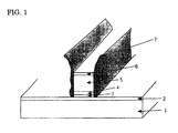
- Fig. 1 is shown a partial cross-sectional view of a semiconductor device that is obtained by forming Al-alloy (Al-Cu) wiring 5 by dry etching using a photoresist film as a mask, and then, ashing by oxygen plasma.
- An oxide film 2 is formed on a silicon substrate 1, and the Al-alloy film 5 serving as wiring is formed on the oxide film 2.
- a resist residue 7 remains on the sidewalls of the Al-alloy film 5.
- a titanium film 3 and titanium nitride films 4, 6 are further formed as barrier metals.
- the semiconductor device having the resist residue as shown in Fig. 1 was immersed in the photoresist stripping composition having each chemical composition shown in Tables 1-4 in a predetermined period of time, rinsed with a super pure water, dried, and then observed under a scanning electron microscope (SEM). The removal of the remaining photoresist film and resist residue, and the corrosion of the aluminum (Cl) wiring were evaluated. The results are shown in Table 1-4. In the following examples and comparative examples, the results of SEM observation was evaluated according to the following ratings.
- the resist residue remaining after dry etching using a reactive gas and ashing can be quite easily removed without corroding the wiring material, etc.
Landscapes
- Physics & Mathematics (AREA)
- General Physics & Mathematics (AREA)
- Photosensitive Polymer And Photoresist Processing (AREA)
- Exposure Of Semiconductors, Excluding Electron Or Ion Beam Exposure (AREA)
Description
- The present invention relates to a photoresist stripping composition for use in the wiring-forming process or electrode-forming process for producing semiconductor elements of semiconductor integrated circuits or liquid crystal displays, and relates to a process of producing semiconductor elements using the photoresist stripping composition.
- Semiconductor integrated circuits have been generally produced by the steps of coating a photoresist composition onto a wiring thin film formed on an inorganic substrate to form a photoresist film; patterning the photoresist film by exposure to light and subsequent development to form a photoresist pattern; etching non-masked portions of the wiring thin film using the photoresist pattern as a mask to form fine circuits; and removing the photoresist film from the inorganic substrate having formed thereon the fine circuits. Alternatively, after forming the fine circuits in the same manner, the photoresist film is ashed and the remaining resist residues are removed from the inorganic substrate having formed thereon the fine circuits.
- Japanese Patent Application Laid-Open Nos.
62-49355 62-95531 5-273768 - Under the recent requirement for ultrafine circuits, the wiring materials are etched under more severe conditions, this being likely to change the quality of the photoresist being used. Also, the resist residue after etching/plasma ashing has a complicated chemical composition. Therefore, the proposed organic amine-based stripping agents have been found to be less effective for removing such resist films and resist residues.
- In a dry etching, sidewall polymers, a kind of resist residues, are formed on the sidewall of etched portions by the interaction between dry etching gas, resist materials and various wiring materials. The known organic amine-based stripping agents mentioned above are also less effective for removing the sidewall polymers.
- Japanese Patent Application Laid-Open Nos.
64-81949 64-81950 6-266119 - The semiconductor elements for semiconductor integrated circuits and liquid crystal displays are recently made of various materials. Therefore, a photoresist stripping agent that does not corrode the inorganic substrate and wiring that are made of various materials have been demanded to be developed.
- An object of the present invention is to solve the above problems in the conventional stripping agents, and to provide a resist stripping composition that is capable of easily removing photoresist films coated on a wiring thin film formed on an inorganic substrate, photoresist films remaining after etching the wiring thin film, and photoresist residues remaining after etching and subsequent ashing, at low temperatures in a short period of time without corroding the inorganic substrate and wiring made of various inorganic materials, thereby ensuring the fine processing for forming high precision circuits.
- As a result of extensive researches in view of the above objects, the inventors have found a photoresist stripping composition that is capable of removing photoresist masks and resist residues remaining after etching and resist residues remaining after etching and subsequent ashing easily in a short period of time without corroding wiring and insulating film formed on an inorganic substrate, thereby ensuring the production of semiconductor fine circuits with a high precision. The present invention has been accomplished based on this finding.
- Thus, the present invention provides a photoresist stripping composition according to claim 1. The photoresist stripping composition may further contain at least one of an organic solvent, an anti-corrosion agent and water.
-
-
Fig. 1 is a partial cross-sectional view showing a semiconductor device obtained by forming Al-alloy wiring by dry etching using a resist film as a mask, and then, ashing by oxygen plasma. - The amine compound usable may include, for example, an alkylamine, an alkanolamine, a polyamine, a hydroxylamine compound and a cyclic amine.
- Examples of the alkyl amines include primary alkylamines such as methylamine, ethylamine, n-propylamine, isopropylamine, n-butylamine, sec-butylamine, isobutylamine, t-butylamine, pentylamine, 2-aminopentane, 3-aminopentane, 1-amino-2-methylbutane, 2-amino-2-methylbutane, 3-amino-2-methylbutane, 4-amino-2-methylbutane, hexylamine, 5-amino-2-methylpentane, heptylamine, octylamine, nonylamine, decylamine, undecylamine, dodecylamine, tridecylamine, tetradecylamine, pentadecylamine, hexadecylamine, heptadecylamine, and octadecylamine; secondary alkylamines such as dimethylamine, diethylamine, dipropylamine, diisopropylamine, dibutylamine, diisobutylamine, di-sec-butylamine, di-t-butylamine, dipentylamine, dihexylamine, diheptylamine, dioctylamine, dinonylamine, didecylamine, methylethylamine, methypropylamine, methylisopropylamine, methylbutylamine, methylisobutylamine, methyl-sec-butylamine, methyl-t-butylamine, methylamylamine, methylisoamylamine, ethylpropylamine, ethylisopropylamine, ethylbutylamine, ethylisobutylamine, ethyl-sec-butylamine, ethyl-t-butylamine, ethylisoamylamine, propylbutylamine, and propylisobutylamine; and tertiary alkylamines such as trimethylamine, triethylamine, tripropylamine, tributylamine, tripentylamine, dimethylethylamine, methyldiethylamine, and methyldipropylamine.
- Examples of the alkanolamines include ethanolamine, N-methylethanolamine, N-ethylethanolamine, N-propylethanolamine, N-butylethanolamine, diethanolamine, isopropanolamine, N-methylisopropanolamine, N-ethylisopropanolamine, N-propylisopropanolamine, 2-aminopropane-1-ol, N-methyl-2-aminopropane-1-ol, N-ethyl-2-aminopropane-1-ol, 1-aminopropane-3-ol, N-methyl-1-aminopropane-3-ol, N-ethyl-1-aminopropane-3-ol, 1-aminobutane-2-ol, N-methyl-1-aminobutane-2-ol, N-ethyl-1-aminobutane-2-ol, 2-aminobutane-1-ol, N-methyl-2-aminobutane-1-ol, N-ethyl-2-aminobutane-1-ol, 3-aminobutane-1-ol, N-methyl-3-aminobutane-1-ol, N-ethyl-3-aminobutane-1-ol, 1-aminobutane-4-ol, N-methyl-1-aminobutane-4-ol, N-ethyl-1-aminobutane-4-ol, 1-amino-2-methylpropane-2-ol, 2-amino-2-methylpropane-1-ol, 1-aminopentane-4-ol, 2-amino-4-methylpentane-1-ol, 2-aminohexane-1-ol, 3-aminoheptane-4-ol, 1-aminooctane-2-ol, 5-aminooctane-4-ol, 1-aminopropane-2,3-diol, 2-aminopropane-1,3-diol, tris(oxymethyl)aminomethane, 1,2-diaminopropane-3-ol, 1,3-diaminopropane-2-ol, and 2-(2-aminoethoxy)ethanol.
- Examples of the polyamines include ethylenediamine, propylenediamine, trimethylenediamine, tetramethylenediamine, 1,3-diaminobutane, 2,3-diaminobutane, pentamethylenediamine, 2,4-diaminopentane, hexamethylenediamine, heptamethylenediamine, octamethylenediamine, nonamethylenediamine, N-methylethylenediamine, N,N-dimethylethylenediamine, trimethylethylenediamine, N-ethylethylenediamine, N,N-diethylethylenediamine, triethylethylenediamine, 1,2,3-triaminopropane, hydrazine, tris(2-aminoethyl)amine, tetra(aminomethyl)methane, diethylenetriamine, triethylenetetramine, tetraethylenepentamine, heptaethyleneoctamine, and nonaethylenedecamine.
- Examples of the hydroxylamine compounds include hydroxylamine, N-methylhydroxylamine, N-ethylhydroxylamine, and N,N-diethylhydroxylamine.
- Examples of the cyclic amines include pyrrole, 2-methylpyrrole, 3-methylpyrrole, 2-ethylpyrrole, 3-ethylpyrrole, 2,3-dimethylpyrrole, 2,4-dimethylpyrrole, 3,4-dimethylpyrrole, 2,3,4-trimethylpyrrole, 2,3,5-trimethylpyrrole, 2-pyrroline, 3-pyrroline, pyrrolidine, 2-methylpyrrolidine, 3-methylpyrrolidine, pyrazole, imidazole, 1,2,3-trizaole, 1,2,3,4-tetrazole, piperidine, 2-pipecoline, 3-pipecoline, 4-pipecoline, 2,4-lupetidine, 2,6-lupetidine, 3,5-lupetidine, piperazine, 2-methylpiperazine, 2,5-dimethylpiperazine, 2,6-dimethylpiperazine, and morpholine.
- The amine compound usable in the present invention is not limited to the amines recited above, and any amine compounds are usable without specific limitation. The amine compounds may be used singly or in combination of two or more.
- Of the amine compounds recited above, preferred are methylamine, ethylamine, propylamine, butylamine, ethanolamine, N-methylethanolamine, N-ethylethanolamine, diethanolamine, isopropanolamine, 2-(2-aminoethoxy)ethanol, ethylenediamine, propylenediamine, butylenediamine, diethylenetriamine, piperazine, and morpholine.
- The organic solvent usable in the present invention is not specifically limited as far as miscible with a mixture of the alkanol amide compound and the amine compound, and preferably a water-soluble organic solvent.
Examples thereof include ether solvents such as ethylene glycol, ethylene glycol monoethyl ether, ethylene glycol monobutyl ether, diethylene glycol monomethyl ether, diethylene glycol monoethyl ether, diethylene glycol monobutyl ether, propylene glycol monomethyl ether, propylene glycol monoethyl ether, propylene glycol monobutyl ether, dipropylene glycol monomethyl ether, dipropylene glycol monoethyl ether, dipropylene glycol monobutyl ether, diethylene glycol dimethyl ether and dipropylene glycol dimethyl ether; amide solvents such as formamide, monomethylformamide, dimethylformamide, monoethylformamide, diethylformamide, acetamide, monomethylacetamide, dimethylacetamide, monoethylacetamide, diethylacetamide, N-metylpyrrolidone and N-ethylpyrrolidone; alcohol solvents such as methyl alcohol, ethyl alcohol, isopropanol, ethylene glycol and propylene glycol; sulfoxide solvents such as dimethyl sulfoxide; sulfone solvents such as dimethyl sulfone, diethyl sulfone, bis(2-hydroxy) sulfone and tetramethylene sulfone; imidazolidinone solvents such as 1,3-dimethyl-2-imidazolidinone, 1,3-diethyl-2-imidazolidinone and 1,3-diisopropyl-2-imidazolidinone; and lactone solvents such as γ-butyrolactone and δ-valerolactone. - Of the above solvents, preferred are dimethyl sulfoxide, N,N-dimethylformamide, N,N-dimethylacetamide, N-methylpyrrolidone, diethylene glycol monomethyl ether, diethylene glycol monobutyl ether, dipropylene glycol monomethyl ether and dipropylene glycol monobutyl ether.
- The photoresist stripping composition of the present invention may further contain an anti-corrosion agent. Examples thereof include phosphoric acid compounds such as 1,2-propanediaminetetramethylene phosphonic acid and hydroxyethane phosphonic acid; caboxylic acids such as ethylenediaminetetraacetic acid, dihydroxyethylglycine, nitrilotriacetic acid, oxalic acid, citric acid, malic acid and tartaric acid; amines such as bipyridine, tetraphenylporphyrin, phenanthroline and 2,3-pyridinediol; oxime compounds such as dimethylglyoxime and diphenylglyoxime; sugar alcohols such as sorbitol and xylitol; aromatic hydroxy compounds such as phenol, cresol, xylenol, pyrocatechol, resorcinol, hydroquinone, pyrogallol, 1,2,4-benzenetriol, salicyl alcohol, p-hydroxybenzyl alcohol, o-hydroxybenzyl alcohol, p-hydroxyphenetyl alcohol, p-aminophenol, m-aminophenol, diaminophenol, aminoresorcinol, p-hydroxybenzoic acid, o-hydroxybenzoic acid, 2,4-dihydroxybenzoic acid, 2,5-dihydroxybenzoic acid, 3,4-dihydroxybenzoic acid, 3,5-dihydroxybenzoic acid and gallic acid.
- These compounds may be used alone or in combination of two or more.
Preferred anti-corrosion agent is the aromatic hydroxy compound, and catechol is more preferred in view of its low cost. - The mixing ratio (weight ratio) of the alkanol amide compound is 0.0001 to 50, preferably 0.005 to 20 based on the amine compound. The concentration of the amine compound in the photoresist stripping composition is 2 to 99.99% by weight, preferably 5 to 95% by weight.
- The use of the organic solvent is not strictly limited. The concentration thereof can be determined depending on the viscosity and specific gravity of the photoresist stripping composition and the conditions of etching process and ashing process. If used, the concentration thereof may be up to 90% by weight of the photoresist stripping composition.
- The addition amount of the anti-corrosion agent is not specifically limited, and preferably 30% by weight or less, more preferably 15% by weight or less of the photoresist stripping composition.
- The photoresist stripping composition may further contain water. The addition amount of water is not specifically limited and may be determined depending on the etching conditions and ashing conditions. Preferably, the addition amount of water is 50% by weight or less of the photoresist stripping composition.
- The inorganic substrate usable in the present invention may include silicon, amorphous silicon, polysilicon, and glass substrate for liquid crystal display. The wiring material may include semiconductor wiring materials such as silicon oxide, silicon nitride, copper, copper alloys, aluminum, aluminum alloys, titanium, titanium-tungsten, titanium nitride, tungsten, tantalum, tantalum compounds, chromium, chromium oxide, chromium alloys, indium-tin-oxide (ITO); and compound semiconductors such as gallium-arsenic, gallium-phosphorus and indium-phosphorus.
- In the production method of a semiconductor element of the present invention, an inorganic substrate is provided thereon with a conductive thin film for circuits, which is then coated with a photoresist composition. The formed photoresist film is patterned by exposure to light. The non-masked portions of the conductive thin film is etched using the patterned photoresist film as a mask. Then, the remaining photoresist film is removed by the photoresist stripping composition mentioned above. After the etching, the ashing treatment may be employed, if desired. The photoresist residue remaining after the ashing treatment can be also removed by the photoresist stripping composition. The ashing treatment referred to herein is a resist removing method in which a photoresist made of an organic polymer is vaporized to CO and CO2 by combustion in oxygen plasma.
- The removal of the remaining photoresist film and photoresist residue by the photoresist stripping composition of the present invention is carried out by contacting the inorganic substrate having the remaining photoresist film and photoresist residue with the photoresist stripping composition at a temperature usually from ordinary temperature to 150°C. To prevent the materials for semiconductor elements form being attacked, the contacting operation is preferably carried out at a temperature as low as possible. By using the photoresist stripping composition of the present invention, the remaining photoresist film and photoresist residue can be removed at low temperatures, particularly, at 70°C or lower. The contacting operation is carried out by spray, application or immersion. The contacting time is preferably 0.5 to 60 min.
- After removal using the photoresist stripping composition, the inorganic substrate having formed thereon circuits may be rinsed with an organic solvent such as alcohol or water, without specific limitation.
- The present invention will be described in more detail with reference to the following examples. However, it should be noted that the scope of the present invention is not limited to the following examples.
- In
Fig. 1 , is shown a partial cross-sectional view of a semiconductor device that is obtained by forming Al-alloy (Al-Cu)wiring 5 by dry etching using a photoresist film as a mask, and then, ashing by oxygen plasma. Anoxide film 2 is formed on a silicon substrate 1, and the Al-alloy film 5 serving as wiring is formed on theoxide film 2. On the sidewalls of the Al-alloy film 5, a resistresidue 7 remains. Atitanium film 3 and titanium nitride films 4, 6 are further formed as barrier metals. - The semiconductor device having the resist residue as shown in
Fig. 1 was immersed in the photoresist stripping composition having each chemical composition shown in Tables 1-4 in a predetermined period of time, rinsed with a super pure water, dried, and then observed under a scanning electron microscope (SEM). The removal of the remaining photoresist film and resist residue, and the corrosion of the aluminum (Cl) wiring were evaluated. The results are shown in Table 1-4. In the following examples and comparative examples, the results of SEM observation was evaluated according to the following ratings. -
- A: Completely removed.
- B: Almost completely removed.
- C: Partially remained unremoved.
- D: Almost all remained unremoved.
-
- A: No corrosion was observed.
- B: Almost no corrosion was observed.
- C: Crater-like or pit-like corrosion was observed.
- D: Whole surface of aluminum wiring was roughened, and Al-Cu layer was recessed.
- By using the photoresist stripping composition of the present invention, the resist residue remaining after dry etching using a reactive gas and ashing can be quite easily removed without corroding the wiring material, etc.
| EXAMPLES | ||||
| 1 | 2 | 3 | 4 | |
| Amine | ||||
| kind | ethanol | ethanol | ethanol | ethanol |
| amine | amine | amine | amine | |
| concentration (wt %) | 70 | 78 | 78 | 75 |
| Alkanol amide | ||||
| kind* | MLAD | MLAD | MLFD | MLAD |
| concentration (wt %) | 3 | 5 | 5 | 8 |
| Organic solvent | ||||
| kind* | DMSO | - | - | - |
| concentration (wt %) | 27 | - | - | - |
| Anti-corrosion agent | ||||
| kind | - | catechol | catechol | catechol |
| concentration (wt %) | - | 5 | 5 | 5 |
| H2O | ||||
| concentration (wt %) | - | 12 | 12 | 12 |
| Stripping conditions | ||||
| temperature (°C) | 55 | 55 | 55 | 55 |
| time (min) | 10 | 3 | 3 | 5 |
| Stripping | A | A | A | A |
| Corrosion | A | A | A | A |
| Note: MLAD = N-methylol acetamide MLFD = N-methylol formamide DMSO = dimethylsulfoxide |
| EXAMPLES | ||||
| 5 | 6 | 7 | 8 | |
| Amine | ||||
| kind | ethanol | ethanol | ethylene | N-methyl |
| amine | amine | diamine | ethanolamine | |
| concentration (wt %) | 75 | 65 | 50 | 78 |
| Alkanol amide | ||||
| kind* | HEAD | MLAD | MLAD | MLAD |
| concentration (wt %) | 8 | 5 | 5 | 5 |
| Organic solvent | ||||
| kind* | - | DGBE | DGBE | - |
| concentration (wt %) | - | 15 | 30 | - |
| Anti-corrosion agent | ||||
| kind | catechol | catechol | EDTA | catechol |
| concentration (wt %) | 5 | 3 | 3 | 5 |
| H2O | ||||
| concentration (wt %) | 12 | 12 | 12 | 12 |
| Stripping conditions | ||||
| temperature (°C) | 55 | 55 | 50 | 55 |
| time (min) | 5 | 5 | 3 | 10 |
| Stripping | A | A | A | A |
| Corrosion | A | A | A | A |
| Note: HEAD = N-(1-hydroxyethyl) acetamide MLAD = N-methylol acetamide DGBE = diethylene glycol monobutyl ether EDTA = ethylenediaminetetraacetic acid |
| EXAMPLES | ||||
| 9 | 10 | 11 | 12 | |
| Amine | ||||
| kind | ethanol | ethanol | ethanol | ethanol |
| amine | amine | amine | amine | |
| concentration (wt %) | 65 | 40 | 73 | 65 |
| Alkanol amide | ||||
| kind* | MLAD | HEAD | HEAD | HEAD |
| concentration (wt %) | 5 | 5 | 10 | 5 |
| Organic solvent | ||||
| kind* | DMSO | DGBE | - | DMAC |
| concentration (wt %) | 15 | 40 | - | 15 |
| Anti-corrosion agent | ||||
| kind | catechol | catechol | catechol | catechol |
| concentration (wt %) | 3 | 3 | 5 | 3 |
| H2O | ||||
| concentration (wt %) | 12 | 12 | 12 | 12 |
| Stripping conditions | ||||
| temperature (°C) | 55 | 55 | 55 | 55 |
| time (min) | 5 | 10 | 5 | 10 |
| Stripping | A | A | A | A |
| Corrosion | A | A | A | A |
| Note: MLAD = N-methylol acetamide HEAD = N-(1-hydroxyethyl) acetamide DMSO = dimethylsulfoxide DGBE = diethylene glycol monobutyl ether DMAC = dimethyl acetamide |
| COMPARATIVE EXAMPLES | ||||
| 1 | 2 | 3 | 4 | |
| Amine | ||||
| kind | ethanol | ethanol | ethanol | N-methyl |
| amine | amine | amine | ethanolamine | |
| concentration (wt %) | 70 | 78 | 65 | 78 |
| Alkanol amide | ||||
| kind* | - | - | - | - |
| concentration (wt %) | - | - | - | - |
| Organic solvent | ||||
| kind* | DMSO | - | DGBE | - |
| concentration (wt %) | 30 | - | 15 | - |
| Anti-corrosion agent | ||||
| kind | - | catechol | catechol | catechol |
| concentration (wt %) | - | 5 | 3 | 5 |
| H2O | ||||
| concentration (wt %) | - | 17 | 17 | 17 |
| Stripping conditions | ||||
| temperature (°C) | 55 | 55 | 55 | 55 |
| time (min) | 10 | 3 | 5 | 10 |
| Stripping | C | B | C | D |
| Corrosion | A | B | B | A |
| Note: DMSO = dimethylsulfoxide DGBE = diethylene glycol monobutyl ether |
Claims (8)
- A photoresist stripping composition comprising an amine compound and at least one alkanol amide compound selected from the group consisting of N-methylol acetamide, N-methylol formamide, N-(1-hydroxyethyl) acetamide, N-(1-hydroxyethyl) formamide, N-methylol urea, N,N'-dimethylol urea, N-methylol acrylamide and N-methylol methacrylamide.
- The photoresist stripping composition according to Claim 1, wherein the amine compound is an alkylamine, an alkanolamine, a polyamine, a hydroxylamine compound or a cyclic amine.
- The photoresist stripping composition according to Claim 1 or 2, further comprising an organic solvent.
- The photoresist stripping composition according to any one of Claims 1 to 3, further comprising an anti-corrosion agent.
- The photoresist stripping composition according to Claim 4, wherein the anti-corrosion agent is an aromatic hydroxy compound.
- The photoresist stripping composition according to Claim 5, wherein the anti-corrosion agent is catechol.
- The photoresist stripping composition according to any one of Claims 1 to 6, further comprising water.
- A method for producing a semiconductor element, comprising the steps of:(1) coating a photoresist composition onto a wiring thin film formed on an inorganic substrate to form a photoresist film;(2) patterning the photoresist film by exposure to light and subsequent development to form a photoresist pattern;(3) etching non-masked portions of the wiring thin film using the photoresist pattern as a mask to obtain the inorganic substrate having formed thereon fine circuits; and(4) removing the remaining photoresist pattern by contacting the inorganic substrate having formed thereon fine circuits with the photoresist stripping composition as defined in any one of Claims 1 to 7 at a temperature from ordinary temperature to 150°C.
Applications Claiming Priority (3)
| Application Number | Priority Date | Filing Date | Title |
|---|---|---|---|
| JP2001197935 | 2001-06-29 | ||
| JP2001197935A JP4810764B2 (en) | 2001-06-29 | 2001-06-29 | Resist stripper composition |
| PCT/JP2002/006216 WO2003003124A1 (en) | 2001-06-29 | 2002-06-21 | Photoresist stripper composition |
Publications (3)
| Publication Number | Publication Date |
|---|---|
| EP1400858A1 EP1400858A1 (en) | 2004-03-24 |
| EP1400858A4 EP1400858A4 (en) | 2006-06-28 |
| EP1400858B1 true EP1400858B1 (en) | 2009-08-19 |
Family
ID=19035458
Family Applications (1)
| Application Number | Title | Priority Date | Filing Date |
|---|---|---|---|
| EP02743687A Expired - Fee Related EP1400858B1 (en) | 2001-06-29 | 2002-06-21 | Photoresist stripper composition |
Country Status (7)
| Country | Link |
|---|---|
| US (1) | US20040081922A1 (en) |
| EP (1) | EP1400858B1 (en) |
| JP (1) | JP4810764B2 (en) |
| KR (1) | KR100907142B1 (en) |
| DE (1) | DE60233406D1 (en) |
| TW (1) | TWI317354B (en) |
| WO (1) | WO2003003124A1 (en) |
Families Citing this family (37)
| Publication number | Priority date | Publication date | Assignee | Title |
|---|---|---|---|---|
| US20050049162A1 (en) * | 2003-08-29 | 2005-03-03 | Schlosser Ted M. | Petroleum-free, ammonia-free cleaner for firearms and ordnance |
| JPWO2005040931A1 (en) * | 2003-10-29 | 2007-04-19 | ナガセケムテックス株式会社 | Composition for stripping photoresist and stripping method |
| KR100663624B1 (en) * | 2004-04-29 | 2007-01-02 | 엘지.필립스 엘시디 주식회사 | Method for manufacturing lcd |
| US8178482B2 (en) * | 2004-08-03 | 2012-05-15 | Avantor Performance Materials, Inc. | Cleaning compositions for microelectronic substrates |
| JP4846301B2 (en) * | 2004-08-30 | 2011-12-28 | サムスン エレクトロニクス カンパニー リミテッド | Thin film transistor substrate manufacturing method and stripping composition |
| KR100594940B1 (en) * | 2004-12-31 | 2006-06-30 | 매그나칩 반도체 유한회사 | Aqueous composition for cleaning photoresist and method of pattern formation using the same |
| US20070251551A1 (en) * | 2005-04-15 | 2007-11-01 | Korzenski Michael B | Removal of high-dose ion-implanted photoresist using self-assembled monolayers in solvent systems |
| KR101088568B1 (en) * | 2005-04-19 | 2011-12-05 | 아반토르 퍼포먼스 머티리얼스, 인크. | Non-aqueous photoresist stripper that inhibits galvanic corrosion |
| KR100705416B1 (en) * | 2005-06-15 | 2007-04-10 | 삼성전자주식회사 | Composition for removing photoresist, method of preparing the composition, method of removing photoresist and method of manufacturing a semiconductor device using the same |
| KR100718532B1 (en) * | 2005-08-13 | 2007-05-16 | 테크노세미켐 주식회사 | Photoresist stripper composition for semiconductor manufacturing |
| DE602006017559D1 (en) | 2005-08-13 | 2010-11-25 | Techno Semichem Co Ltd | FOTORESIST DISTANCE COMPOSITION FOR SEMICONDUCTOR MANUFACTURING |
| US20070243773A1 (en) * | 2005-10-28 | 2007-10-18 | Phenis Michael T | Dynamic multi-purpose composition for the removal of photoresists and method for its use |
| US7632796B2 (en) * | 2005-10-28 | 2009-12-15 | Dynaloy, Llc | Dynamic multi-purpose composition for the removal of photoresists and method for its use |
| US9329486B2 (en) | 2005-10-28 | 2016-05-03 | Dynaloy, Llc | Dynamic multi-purpose composition for the removal of photoresists and method for its use |
| US8263539B2 (en) * | 2005-10-28 | 2012-09-11 | Dynaloy, Llc | Dynamic multi-purpose composition for the removal of photoresists and methods for its use |
| KR101330509B1 (en) * | 2005-12-01 | 2013-11-15 | 미츠비시 가스 가가쿠 가부시키가이샤 | Cleaning solution for semiconductor device or display device, and cleaning method |
| US20070179072A1 (en) * | 2006-01-30 | 2007-08-02 | Rao Madhukar B | Cleaning formulations |
| US7655608B2 (en) * | 2007-08-03 | 2010-02-02 | Dynaloy, Llc | Reduced metal etch rates using stripper solutions containing a copper salt |
| US8551682B2 (en) * | 2007-08-15 | 2013-10-08 | Dynaloy, Llc | Metal conservation with stripper solutions containing resorcinol |
| TWI450052B (en) * | 2008-06-24 | 2014-08-21 | Dynaloy Llc | Stripper solutions effective for back-end-of-line operations |
| WO2010061701A1 (en) * | 2008-11-28 | 2010-06-03 | 出光興産株式会社 | Anti-corrosive photoresist-removing agent composition |
| US8697912B2 (en) * | 2009-01-06 | 2014-04-15 | Showa Denko K.K. | N-(1-hydroxyethyl) carboxamide compound and process for producing same |
| US8614053B2 (en) | 2009-03-27 | 2013-12-24 | Eastman Chemical Company | Processess and compositions for removing substances from substrates |
| US8309502B2 (en) * | 2009-03-27 | 2012-11-13 | Eastman Chemical Company | Compositions and methods for removing organic substances |
| US8444768B2 (en) | 2009-03-27 | 2013-05-21 | Eastman Chemical Company | Compositions and methods for removing organic substances |
| KR101829399B1 (en) * | 2010-03-04 | 2018-03-30 | 삼성전자주식회사 | photosensitive-resin remover composition and method of fabricating semiconductor device using the same |
| TWI539493B (en) | 2010-03-08 | 2016-06-21 | 黛納羅伊有限責任公司 | Methods and compositions for doping silicon substrates with molecular monolayers |
| KR101721262B1 (en) * | 2010-09-01 | 2017-03-29 | 동우 화인켐 주식회사 | Resist stripper composition and a method of stripping resist using the same |
| US20120073607A1 (en) * | 2010-09-27 | 2012-03-29 | Eastman Chemical Company | Polymeric or monomeric compositions comprising at least one mono-amide and/or at least one diamide for removing substances from substrates and methods for using the same |
| US8987181B2 (en) | 2011-11-08 | 2015-03-24 | Dynaloy, Llc | Photoresist and post etch residue cleaning solution |
| US9029268B2 (en) | 2012-11-21 | 2015-05-12 | Dynaloy, Llc | Process for etching metals |
| US9158202B2 (en) | 2012-11-21 | 2015-10-13 | Dynaloy, Llc | Process and composition for removing substances from substrates |
| CN103336412B (en) * | 2013-07-03 | 2017-02-08 | 北京科华微电子材料有限公司 | Novel photoresist stripper and application technology thereof |
| US9957469B2 (en) | 2014-07-14 | 2018-05-01 | Versum Materials Us, Llc | Copper corrosion inhibition system |
| CN107078044B (en) | 2014-11-13 | 2020-06-19 | 三菱瓦斯化学株式会社 | Cleaning liquid for semiconductor element with suppressed damage of cobalt, and method for cleaning semiconductor element using same |
| JP6808730B2 (en) * | 2016-06-03 | 2021-01-06 | 富士フイルム株式会社 | Treatment liquid, substrate cleaning method and resist removal method |
| JP6160893B1 (en) * | 2016-09-30 | 2017-07-12 | パナソニックIpマネジメント株式会社 | Resist stripper |
Family Cites Families (11)
| Publication number | Priority date | Publication date | Assignee | Title |
|---|---|---|---|---|
| ZA87922B (en) * | 1986-02-28 | 1987-09-30 | Macdermid Inc | Photoresist stripper composition |
| JPH0769618B2 (en) * | 1987-09-25 | 1995-07-31 | 旭化成工業株式会社 | Stripping agent for photoresist |
| US5102777A (en) * | 1990-02-01 | 1992-04-07 | Ardrox Inc. | Resist stripping |
| JP2911792B2 (en) * | 1995-09-29 | 1999-06-23 | 東京応化工業株式会社 | Stripper composition for resist |
| JP3373105B2 (en) * | 1996-03-11 | 2003-02-04 | 富士フイルムアーチ株式会社 | Photoresist stripper |
| JP3682339B2 (en) * | 1996-05-21 | 2005-08-10 | 日東電工株式会社 | Resist removal adhesive sheet and resist removal method |
| JP3891735B2 (en) * | 1998-08-05 | 2007-03-14 | 三星電子株式会社 | Resist removing agent comprising alkoxy N-hydroxyalkylalkanamide, resist removing composition, production method thereof, and resist removal method using them |
| KR100335484B1 (en) * | 1998-08-05 | 2002-05-04 | 윤종용 | Use of an Alkoxy N-Hydroxyalkyl Alkanamide as Resist Removing Agent, Composition for Removing Resist, Method for Preparing the Same and Resist Removing Method Using the Same |
| JP4224651B2 (en) * | 1999-02-25 | 2009-02-18 | 三菱瓦斯化学株式会社 | Resist stripper and method for manufacturing semiconductor device using the same |
| JP2001022095A (en) | 1999-07-02 | 2001-01-26 | Nippon Zeon Co Ltd | Positive type resist removing solution |
| JP2001055095A (en) * | 1999-08-17 | 2001-02-27 | Takashimaya Nippatsu Kogyo Co Ltd | Vehicular door trim |
-
2001
- 2001-06-29 JP JP2001197935A patent/JP4810764B2/en not_active Expired - Lifetime
-
2002
- 2002-06-21 KR KR1020037002922A patent/KR100907142B1/en active IP Right Grant
- 2002-06-21 WO PCT/JP2002/006216 patent/WO2003003124A1/en active Application Filing
- 2002-06-21 US US10/363,064 patent/US20040081922A1/en not_active Abandoned
- 2002-06-21 EP EP02743687A patent/EP1400858B1/en not_active Expired - Fee Related
- 2002-06-21 DE DE60233406T patent/DE60233406D1/en not_active Expired - Lifetime
- 2002-06-27 TW TW091114143A patent/TWI317354B/en not_active IP Right Cessation
Also Published As
| Publication number | Publication date |
|---|---|
| JP4810764B2 (en) | 2011-11-09 |
| DE60233406D1 (en) | 2009-10-01 |
| JP2003015320A (en) | 2003-01-17 |
| KR100907142B1 (en) | 2009-07-09 |
| WO2003003124A1 (en) | 2003-01-09 |
| US20040081922A1 (en) | 2004-04-29 |
| EP1400858A4 (en) | 2006-06-28 |
| KR20040014975A (en) | 2004-02-18 |
| EP1400858A1 (en) | 2004-03-24 |
| TWI317354B (en) | 2009-11-21 |
Similar Documents
| Publication | Publication Date | Title |
|---|---|---|
| EP1400858B1 (en) | Photoresist stripper composition | |
| KR100672102B1 (en) | Resist stripping agent and process of producing semiconductor devices using the same | |
| US7049275B2 (en) | Photoresist stripping composition and cleaning composition | |
| US7078371B2 (en) | Cleaning composition | |
| US20060270574A1 (en) | Photoresist stripping agent | |
| JP3048207B2 (en) | Detergent composition containing nucleophilic amine compound having reduction and oxidation potential and method for cleaning substrate using the same | |
| US20040256358A1 (en) | Method for releasing resist | |
| JP4359754B2 (en) | Substrate cleaning agent | |
| JP2003140364A (en) | Resist removing solution for copper wiring board | |
| JP4867092B2 (en) | Resist stripper composition | |
| JP4035701B2 (en) | Resist stripper and method of using the same | |
| JP4320865B2 (en) | Resist stripper composition and method for producing semiconductor device using the same. | |
| JP2003156859A (en) | Photoresist remover composition and removing method | |
| JP4639567B2 (en) | Photoresist stripping composition | |
| JP4577474B2 (en) | Resist stripper composition | |
| JP2003140365A (en) | Method for using resist removing solution |
Legal Events
| Date | Code | Title | Description |
|---|---|---|---|
| PUAI | Public reference made under article 153(3) epc to a published international application that has entered the european phase |
Free format text: ORIGINAL CODE: 0009012 |
|
| 17P | Request for examination filed |
Effective date: 20030208 |
|
| AK | Designated contracting states |
Kind code of ref document: A1 Designated state(s): AT BE CH CY DE DK ES FI FR GB GR IE IT LI LU MC NL PT SE TR |
|
| A4 | Supplementary search report drawn up and despatched |
Effective date: 20060529 |
|
| 17Q | First examination report despatched |
Effective date: 20080623 |
|
| GRAP | Despatch of communication of intention to grant a patent |
Free format text: ORIGINAL CODE: EPIDOSNIGR1 |
|
| GRAS | Grant fee paid |
Free format text: ORIGINAL CODE: EPIDOSNIGR3 |
|
| GRAA | (expected) grant |
Free format text: ORIGINAL CODE: 0009210 |
|
| AK | Designated contracting states |
Kind code of ref document: B1 Designated state(s): DE FR GB IT |
|
| REG | Reference to a national code |
Ref country code: GB Ref legal event code: FG4D |
|
| REF | Corresponds to: |
Ref document number: 60233406 Country of ref document: DE Date of ref document: 20091001 Kind code of ref document: P |
|
| PLBE | No opposition filed within time limit |
Free format text: ORIGINAL CODE: 0009261 |
|
| STAA | Information on the status of an ep patent application or granted ep patent |
Free format text: STATUS: NO OPPOSITION FILED WITHIN TIME LIMIT |
|
| 26N | No opposition filed |
Effective date: 20100520 |
|
| PGFP | Annual fee paid to national office [announced via postgrant information from national office to epo] |
Ref country code: FR Payment date: 20100622 Year of fee payment: 9 |
|
| PGFP | Annual fee paid to national office [announced via postgrant information from national office to epo] |
Ref country code: IT Payment date: 20100626 Year of fee payment: 9 |
|
| PGFP | Annual fee paid to national office [announced via postgrant information from national office to epo] |
Ref country code: DE Payment date: 20100816 Year of fee payment: 9 Ref country code: GB Payment date: 20100401 Year of fee payment: 9 |
|
| GBPC | Gb: european patent ceased through non-payment of renewal fee |
Effective date: 20110621 |
|
| PG25 | Lapsed in a contracting state [announced via postgrant information from national office to epo] |
Ref country code: IT Free format text: LAPSE BECAUSE OF NON-PAYMENT OF DUE FEES Effective date: 20110621 |
|
| REG | Reference to a national code |
Ref country code: FR Ref legal event code: ST Effective date: 20120229 |
|
| REG | Reference to a national code |
Ref country code: DE Ref legal event code: R119 Ref document number: 60233406 Country of ref document: DE Effective date: 20120103 |
|
| PG25 | Lapsed in a contracting state [announced via postgrant information from national office to epo] |
Ref country code: DE Free format text: LAPSE BECAUSE OF NON-PAYMENT OF DUE FEES Effective date: 20120103 Ref country code: FR Free format text: LAPSE BECAUSE OF NON-PAYMENT OF DUE FEES Effective date: 20110630 |
|
| PG25 | Lapsed in a contracting state [announced via postgrant information from national office to epo] |
Ref country code: GB Free format text: LAPSE BECAUSE OF NON-PAYMENT OF DUE FEES Effective date: 20110621 |