EP1398818A2 - Charged particle beam apparatus and irradiation method - Google Patents
Charged particle beam apparatus and irradiation method Download PDFInfo
- Publication number
- EP1398818A2 EP1398818A2 EP03020626A EP03020626A EP1398818A2 EP 1398818 A2 EP1398818 A2 EP 1398818A2 EP 03020626 A EP03020626 A EP 03020626A EP 03020626 A EP03020626 A EP 03020626A EP 1398818 A2 EP1398818 A2 EP 1398818A2
- Authority
- EP
- European Patent Office
- Prior art keywords
- objective lens
- lens
- focusing
- aberration
- sample
- Prior art date
- Legal status (The legal status is an assumption and is not a legal conclusion. Google has not performed a legal analysis and makes no representation as to the accuracy of the status listed.)
- Granted
Links
Images









Classifications
-
- H—ELECTRICITY
- H01—ELECTRIC ELEMENTS
- H01J—ELECTRIC DISCHARGE TUBES OR DISCHARGE LAMPS
- H01J37/00—Discharge tubes with provision for introducing objects or material to be exposed to the discharge, e.g. for the purpose of examination or processing thereof
- H01J37/02—Details
- H01J37/04—Arrangements of electrodes and associated parts for generating or controlling the discharge, e.g. electron-optical arrangement or ion-optical arrangement
- H01J37/153—Electron-optical or ion-optical arrangements for the correction of image defects, e.g. stigmators
-
- H—ELECTRICITY
- H01—ELECTRIC ELEMENTS
- H01J—ELECTRIC DISCHARGE TUBES OR DISCHARGE LAMPS
- H01J2237/00—Discharge tubes exposing object to beam, e.g. for analysis treatment, etching, imaging
- H01J2237/15—Means for deflecting or directing discharge
- H01J2237/1506—Tilting or rocking beam around an axis substantially at an angle to optical axis
-
- H—ELECTRICITY
- H01—ELECTRIC ELEMENTS
- H01J—ELECTRIC DISCHARGE TUBES OR DISCHARGE LAMPS
- H01J2237/00—Discharge tubes exposing object to beam, e.g. for analysis treatment, etching, imaging
- H01J2237/153—Correcting image defects, e.g. stigmators
- H01J2237/1534—Aberrations
-
- H—ELECTRICITY
- H01—ELECTRIC ELEMENTS
- H01J—ELECTRIC DISCHARGE TUBES OR DISCHARGE LAMPS
- H01J2237/00—Discharge tubes exposing object to beam, e.g. for analysis treatment, etching, imaging
- H01J2237/26—Electron or ion microscopes
- H01J2237/28—Scanning microscopes
Definitions
- the present invention relates to a charged-particle beam apparatus employing a charged particle beam such as an electron beam or ion beam.
- the invention relates to a charged particle beam apparatus suitable for obtaining high-resolution images with a minimum loss of resolution in cases where the charged particle beam is inclined with respect to a sample.
- a sample is scanned with a narrowly focused beam of charged particles in order to obtain desired information from the sample (such as a sample image).
- desired information such as a sample image.
- An inclined sample image can be generally obtained by tilting the sample stage.
- the need to tilt the charged particle beam is more practical to tilt the charged particle beam relative to the sample than to mechanically tilt the sample stage, from the viewpoint of preventing a field of view error at higher magnification ratios, or increasing the rate at which inclined sample images are obtained.
- JP Utility Model Publication (Kokai) No. 55-48610 U (1980) and JP Patent Publication (Kokai) No. 2-33843 A (1990) disclose techniques for inclining a charged particle beam while maintaining the high resolution condition of the system. These techniques cause a charged particle beam to be incident on an objective lens off the axis thereof, and utilize the focusing effect (turning-back effect) of the objective lens.
- JP Patent Publication (Kokai) No. 2000-348658 A discloses a technique employing deflecting means in two stages for deflecting a charged particle beam in opposite directions in the focusing magnetic field of an objective lens.
- JP Patent Publication (Kokai) No. 2001-15055 A discloses that deflecting means for passing the charged particle beam off the axis of an objective lens is disposed closer to an electron source than the objective lens.
- Chromatic aberrations (off-axis chromatic aberrations) produced off the axis of the objective lens are corrected by a Wiener filter disposed closer to the electron source than the objective lens, thus reducing the deterioration in resolution when the charged particle beam is inclined.
- WO 01/33603 discloses a technique whereby a Wiener filter for generating a perpendicular electromagnetic field in arbitrarily chosen two-dimensional directions perpendicular to the optical axis is disposed on the optical axis closer to an electron source than an objective lens in order to correct for off-axis chromatic aberrations in arbitrary directions.
- JP Kokai 2000-348658 A in which the charged particle beam is deflected in two stages in the magnetic field of the objective lens, has the problem that high resolution cannot be obtained when adapted to those systems in which the objective lens magnetic field is caused to leak towards the sample in order to obtain high resolution.
- Such systems are becoming increasingly common in recent years.
- the aforementioned problem is due to the fact that the distance between the magnetic poles of the objective lens and the sample has to be increased so that the two-stage deflection means can be disposed therebetween.
- JP Kokai 2000-348658 in which four magnetic poles for the objective lens are provided, and in which the combination of the magnetic poles can be switched depending on whether the purpose is high-resolution observation or the inclination of the charged-particle beam.
- axial misalignment among magnetic poles or other various problems such as magnification error, axial misalignment, variations in scan conditions, etc.
- the off-axis chromatic aberration produced as a charged particle beam is incident on an objective lens off the axis thereof is corrected using a Wiener filter.
- a Wiener filter is not capable of removing the coma aberration, resulting in a decrease in resolution in cases where the charged particle beam is inclined at large angles or when the charged particle beam is inclined at relatively high acceleration voltages.
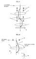
- FIG. 2 the aberrations produced when the charged particle beam is inclined towards a sample using the turning-back effect of an objective lens will be described.
- a beam 4 is deflected by a beam inclination angle control coil 51 at the object point of an objective lens 7 such that the beam is incident on the objective lens 7 off its axis.
- the beam 4 is inclined towards a sample 10 due to the focusing effect of the objective lens 7.
- the field of view does not move even if the beam is inclined.
- the aberration of the objective lens that is produced when the object point is on the optical axis consists of spherical aberration and on-axis chromatic aberration.
- the aberration ( ⁇ w i ) produced by the objective lens can be expressed by a polynomial (1) shown below as a function of a trajectory inclination (w' i ) on the sample.
- a differential equation with respect to z will be herein indicated by a prime (""').
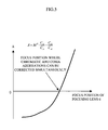
- Fig. 3 shows the condition of the beam in a trajectory curve coordinate system (w' i -coordinate system) on the sample.
- the horizontal axis in Fig. 3 indicates the gradient of the trajectory in the X-direction on the image surface, while the vertical axis indicates the gradient of the trajectory in the Y-direction.
- the description has primes, as mentioned above.
- the circular figure (beam region) in Fig. 3 indicates the region of a set of trajectories of the primary beam having various gradients produced by the focusing effect of the lens.
- Equation (5) can be expanded to give equation (6), in which it will be seen that Seidel aberrations (spherical aberration, coma aberration, astigmatism, field curvature aberration, and distortion) and on-axis and off-axis chromatic aberrations are produced by the beam inclination (whereby the trajectory is displaced off axis) in the system in which originally there was only an on-axis aberration.
- Seidel aberrations spherical aberration, coma aberration, astigmatism, field curvature aberration, and distortion
- on-axis and off-axis chromatic aberrations are produced by the beam inclination (whereby the trajectory is displaced off axis) in the system in which originally there was only an on-axis aberration.
- ⁇ w i C si ⁇ ( w ' f w ' f w ' f + w ' t w ' f w ' f + 2 w' t w ' f w ' f + 2 w ' t w ' t w' f + w ' t w ' t w' f + w ' t w ' t w ' f + w ' t w ' t w ' t ) + C ci ⁇ ⁇ i ⁇ ( w ' t + w ' f )
- terms containing w' t are aberrations produced by the inclination of the beam, which are coma aberration, astigmatism, field curvature aberration, distortion, and off-axis chromatic aberration.
- coma aberration, astigmatism, field curvature aberration, distortion, and off-axis chromatic aberration are aberrations produced by the inclination of the beam.
- ⁇ i of the energy width ⁇ V namely, coma aberration, astigmatism, field curvature aberration, and off-axis chromatic aberration
- astigmatism can be easily corrected by means of a conventional astigmatism correction coil.
- the field curvature aberration which is a focusing error due to beam inclination, can be eliminated by correcting the focusing condition (objective lens current).
- the distortion which is due to the displacement of the irradiated position caused by the beam inclination, can be eliminated by correcting the irradiated position in accordance with the beam inclination.
- the remaining aberrations to be considered are the off-axis chromatic aberration and the coma aberration, which both increase in proportion to the angle of beam inclination (w' t ).
- the object of the invention is to provide a charged particle beam apparatus capable of eliminating the above-described off-axis chromatic aberration and coma aberration in a practical and easy manner. This will allow the beam to be inclined at large angles while preventing the lowering of resolution.
- the apparatus includes at least two stages of focusing lenses including an objective lens, and deflection means for causing the beam to be incident on each of the lenses off the axis thereof.
- the off-axis aberrations (off-axis chromatic aberration and/or coma aberration) produced by the lenses are made to cancel each other out, so that the sum of the off-axis aberrations produced by the lenses is zero or close to zero.
- the apparatus further includes means for controlling astigmatism in accordance with the beam inclination angle. This allows the astigmatism, which varies depending on the beam inclination angle, to be corrected.
- the focal length of the objective lens may be controlled in accordance with the beam inclination angle.
- an irradiated position error may be corrected in accordance with the beam inclination angle.
- an aperture mechanism may be provided in place of the deflection means so that the passage of the beam can be limited. This causes the beam to be incident on the lenses effectively off the axes thereof.
- inclined observation images can be obtained with high resolution without the influences of off-axis chromatic aberration, coma aberration, or astigmatism, even when the beam is inclined by the focusing effect of the objective lens.
- Fig. 1 shows a diagram of a scanning electron microscope as an example of the invention.
- a voltage is applied across a cathode 1 and a first anode 2 by a high-voltage control power supply 20 controlled by a computer 40.
- a primary electron beam 4 is drawn from the cathode 1 with a certain emission current.
- An acceleration voltage is applied across the cathode 1 and a second anode 3 by the high-voltage control power supply 20 under the control of the computer 40.
- the primary electron beam 4 emitted by the cathode 1 is accelerated by the acceleration voltage before arriving at a lens system in a subsequent stage.
- the primary electron beam 4 is then focused by a focusing lens 5 controlled by a lens control power supply 21.
- the beam is focused on a sample 10 as a minute spot by a focusing lens 6 controlled by a lens control power supply 22 and by an objective lens 7 controlled by an objective lens control power supply 23.
- the objective lens 7 may be of any desired type, such as an in-lens type, out-lens type, or snorkel (semi in-lens) type.
- a retarding type may be employed, whereby the primary electron beam is decelerated by applying a negative voltage to the sample.
- each of the lenses may be formed by an electrostatic lens comprised of a plurality of electrodes.
- the primary electron beam 4 is made to scan the sample 10 two dimensionally by a scanning coil 9 controlled by a scanning coil control power supply 24.
- a secondary signal 12 such as secondary electrons emitted by the sample 10 as it is irradiated with the primary electron beam proceeds above the objective lens 7 where the secondary signal is separated from primary electrons by a perpendicular electromagnetic field generator 11 for secondary signal separation.
- the secondary signal is then detected by a secondary signal detector 13.
- the signal detected by the secondary signal detector 13 is amplified by a signal amplifier 14, transferred to an image memory 25, and is then displayed on an image display device 26 as a sample image.
- Deflection coils 51 are disposed in two stages at the same location as the scanning coil 9.
- the position of the primary electron beam 4 incident on the objective lens can be controlled two dimensionally by the deflection coils 51 under the control of an inclination control power supply 31 such that the object point of the objective lens is the point of deflection.
- the beam can be inclined with respect to the optical axis of the objective lens.
- An astigmatism correction coil 53 is disposed near the focusing lens 6 and is controlled by an astigmatism correction power supply 33 in accordance with the degree of beam inclination.
- Other deflection coils 52 are disposed in two stages between the focusing lens 6 and the aperture plate 8.
- the position of the primary electron beam 4 incident on the focusing lens 6 can be controlled two dimensionally by an aberration control power supply 32 such that the object point of the focusing lens 6 is the point of deflection.
- a control signal can be caused to flow into the deflection coils 51 for two dimensionally controlling the position of irradiation of the sample by the primary electron beam.
- the sample 10 can be transported by the sample stage 15 in at least two directions (X and Y directions) in a plane perpendicular to the primary electron beam.
- Various instructions can be entered via an input device 42 concerning, for example, image acquisition conditions (such as scan speed and acceleration voltage), beam inclination conditions (such as the direction and angle of inclination), the output of images, and the storage of images in a storage device 41.
- Fig. 4 shows a principal portion of the microscope.
- the primary beam 4 is deflected by the deflection coils 52 (to be hereafter referred to as aberration control coils) such that the object point of the focusing lens 6 is the point of deflection.
- the deflection coils 52 to be hereafter referred to as aberration control coils
- an aberration with the same property as that obtained when the beam is inclined can be produced by the focusing lens 6.
- the beam inclination condition (condition k) of the focusing lens 6 for canceling the off-axis chromatic aberration produced by the objective lens 7 is given by equation (18) from equation (17).
- the value of k becomes positive because the optical magnification value M is a negative value in the configuration of Fig. 4.
- the beam should only be inclined by the focusing lens 6 by an angle 0.2 times the angle of inclination of the beam by the objective lens 7.
- the angle of inclination of the beam by the objective lens 7 is proportional to the current flowing in the deflection coils 51 (to be hereafter referred to as a beam inclination angle control coil)
- the angle of inclination of the beam by the focusing lens 6 is proportional to the current in the aberration control coil 52, it is possible to preset the relationship between the current in the aberration control coil 52 and the corresponding angle of inclination of the beam by the focusing lens 6 by registering the relationship in the storage device 41, for example.
- the beam inclination angle control power supply 31 and the aberration control power supply 32 can be controlled by the computer 40 such that the proportional relationship in current between the beam inclination angle control coil 51 and the aberration control coil 52 satisfies the condition k in equation (18).
- the value of k is generally different from that in equation (18), so that, if the value of k in equation (20) is selected, equation (18) would not be satisfied, resulting in the development of a chromatic aberration as the beam is inclined.
- equation (18) would not be satisfied, resulting in the development of a chromatic aberration as the beam is inclined.
- the ratio in magnitude between the chromatic aberration and the coma aberration produced when the beam is inclined by the objective lens 7 does not correspond to that between the chromatic aberration and the coma aberration produced when the beam is inclined by the focusing lens 6.
- the beam inclination angle control coil 51 and the aberration control coil 52 are controlled in tandem such that the condition of equation (18) can be satisfied.
- the beam inclination angle control coil 51 and the aberration control coil 52 are controlled in association with one another such that the condition of equation (20) is satisfied.
- the boundary acceleration voltage between the chromatic aberration dominance and the coma aberration dominance is not limited to 5 kV, as the voltage depends on the spherical aberration coefficient and the on-axis chromatic aberration coefficient of the objective lens, as well as the energy width of the primary electron beam.
- the optimum control condition of the aberration control coil 52 is proportional to the beam inclination angle. Accordingly, in the present embodiment, appropriate conditions for specific beam inclination angles are preset, and the beam inclination angle control coil 51 and the aberration control coil 52 are controlled by determining the association condition therebetween through calculating the control condition for a given beam inclination angle.
- off-axis chromatic aberration and the coma aberration have the same degree of influence when the beam is inclined, or when the beam inclination angle is large, such as 5° or more, for example, it is necessary to correct the off-axis chromatic aberration and the coma aberration at the same time.
- equations (18) and (20) In order to correct the off-axis chromatic aberration and the coma aberration at the same time, equations (18) and (20) must have the same value for k. To satisfy this condition, conditions such as the optical magnification (lateral magnification) of the objective lens must be set. These conditions are given by equation (22), which is derived from a relational expression (21) well known in electronic-optical theories.
- This focus position is a condition that satisfies equation (22), and that focus position can be determined experimentally or by simulation.
- the excitation condition for the focusing lens 6 is set such that the relationship of equation (21) is satisfied, while the beam inclination angle control coil 51 and the aberration control coil 52 are controlled in conjunction with each other such that the relationship of equation (23) is satisfied.
- a focusing position of the focusing lens 6 for realizing a value of M that allows equation (22) to be satisfied is obtained in advance by simulation or experiment, and the obtained value is registered in the storage device 41 (step 11).
- a value of k that satisfies equation (23) is calculated in advance and registered in the storage device 41 (step 12).
- the value of k may be obtained in advance by experiment or simulation.
- a relationship between the angle of inclination of the beam by the objective lens 7 and the current in the beam inclination angle control coil 51 is obtained in advance by experiment or simulation and registered in the storage device 41 (step 13).
- a relationship between the angle of inclination of the beam by the focusing lens 6 and the current in the aberration control coil 52 is obtained in advance by experiment or simulation and is registered in the storage device 41 (step 14). Then, based on the value of k that satisfies equation (23), a relationship between the current in the beam inclination angle control coil 51 and that in the aberration control coil 52 is obtained and registered in the storage device 41 (step 15).
- the computer 40 sets the current for the beam inclination angle control coil 51 based on the relationship registered in step 13 and the beam inclination angle (step 16).
- the computer 40 further sets the current for the aberration control coil 52 corresponding to the beam inclination angle control coil 51 based on the relationship registered in step 15 (step 17).
- the astigmatism correction coil and the objective lens current are further controlled in accordance with the beam inclination.
- the astigmatism produced by the inclination of the beam increases in proportion to the square of the beam inclination angle (w' t ).
- the beam inclination angle (w' t ) is proportional to the current in the beam inclination angle control coil 51.
- the operating conditions of the astigmatism corrector 53 for correcting astigmatism as shown in Fig. 9 are preset by registering them in the storage device 41, for example, with respect to a plurality of predetermined conditions for the current in the beam inclination angle control coil 51.
- the astigmatism produced by the inclination of the beam is given as the difference between the amount of astigmatism correction (Isx0, Isy0) at zero beam inclination angle (when the current in the beam inclination angle control coil 51 is zero) and the amount of astigmatism correction at a given beam inclination angle.
- the computer 40 controls the current (Isx, Isy) for the astigmatism correction coil 53 in conjunction with a given current (Ix, Iy) for the beam inclination angle control coil 51 in the following manner:
- the astigmatism correction coil 53 is set such that astigmatism can be automatically corrected when the beam inclination angle is controlled by setting the current for the beam inclination angle control coil 51. Further, a focusing current (objective lens current) error ⁇ Io1 that occurs when the current (Ix, Iy) for the beam inclination angle control coil 51 is changed from (0, 0) to (Ix0, 0), and a focusing current error ⁇ Io2 that occurs when (Ix, Iy) is changed from (0, 0) to (0, Iy0) are registered in the storage device 41.
- the focusing error can be automatically corrected even when the beam inclination angle is controlled by setting the current for the beam inclination angle control coil 51.
- Fig. 7 shows the fourth embodiment in which the focusing lens 6 is composed of two lenses.
- the spherical aberration in the focusing lens In order to produce an aberration that cancels the coma aberration produced by the objective lens due to the beam inclination in the focusing lens, which is disposed closer the electron source than the objective lens, the spherical aberration in the focusing lens must be increased. This is because, as shown by equation (23), the contribution (aberration correction amount) of the spherical aberration in the focusing lens to the final point of focus decreases in proportion to the cube of the optical magnification (M ⁇ 1) of the objective lens.
- a lens 61 with a small geometric aberration such as spherical aberration, is used in combination with a lens 62 with a large geometric aberration, so that high resolution applications and the beam inclining function can be realized simultaneously in a compatible manner.
- the lens 61 (having magnetic poles with a large opening diameter) and the lens 62 (having magnetic poles with little gap with the opening diameter) with a large geometric aberration can be switched depending on purposes.
- the high-resolution lens 61 with a small geometric aberration is used for high-resolution observation purposes, while turning off the lens 62 with a large geometric aberration.
- the lens 62 with a large geometric aberration is used in cases where the beam is inclined, while turning off the high-resolution lens 61.
- the axial misalignment caused by the switching of the magnetic poles can be solved by providing the aberration control coil 63 with an additional function as an alignment coil for correcting the axial misalignment.
- the chromatic aberration produced by the objective lens upon inclination of the beam can be corrected using a plurality of lenses.
- the chromatic aberration produced when the beam is inclined by the objective lens consists of X and Y components corresponding to the direction of the inclination of the beam. This aberration is produced not only in the objective lens but also in any focusing lens as long as the beam is inclined. Its magnitude, however, varies depending on the shape of the magnetic poles of the lens and/or the operating conditions (such as the focal length).
- the chromatic aberration can be corrected if the (vector) sum of the chromatic aberration produced by each lens and the chromatic aberration produced by the objective lens is returned back to zero, as shown in Fig. 8. Accordingly, it does not matter how many lenses are used for correction; what is important is that the vector sum of the chromatic aberrations is zero. The same can be said for the coma aberration, whose direction and magnitude correspond to the inclination of the beam. Thus, the principle of correction of the chromatic aberration depicted in Fig. 8 can be similarly applied to the correction of the coma aberration.
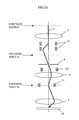
- Figs. 10 to 18 are directed to the control of trajectory in order to make the sum of aberrations produced by a plurality of lenses including an objective lens zero when the beam is inclined by the objective lens.
- Fig. 10 shows an example of trajectory control in a case where one deflector is disposed between the focusing lens 6 and the aperture 8.
- the aberration control coil 52 composed of deflectors disposed in two stages between the aperture 8 and the focusing lens 5 creates a condition such that the primary electron beam 4 passes through the center of the opening of the aperture 8 in an inclined manner.
- the trajectory of the electron beam is then controlled by a deflector 521 disposed between the aperture 8 and the focusing lens 6 such that the point of deflection of the primary electron beam 4 as seen from the focusing lens 6 is at a focus point A of the focusing lens 5.
- a focusing point B of the focusing lens 6 is coincident with the deflecting point of the beam inclination angle control coil 51, and the primary electron beam 4 is inclined by the operation of the beam inclination angle control coil 51 and the objective lens 7.
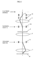
- Fig. 11 shows an example of trajectory control in a case where the deflectors cannot be disposed between the focusing lens 6 and the aperture 8.
- the trajectory of the primary electron beam 4 is controlled by an aberration control coil 52 composed of deflectors disposed in two stages between the focusing lens 5 and the electron source, such that the point of deflection of the primary electron beam 4 is apparently coincident with the position of the electron source.
- the direction of the aberration produced by the focusing lens 5 is reversed by the focusing lens 6. Accordingly, in order to cancel the aberration produced by the objective lens 7, the direction of displacement of the trajectory of the primary electron beam 4 as it passes through the focusing lens 5 (namely the direction of the aberration) is reversed with respect to that in the case of Fig. 10.
- the position of a focusing point A of the focusing lens 5 is coincident with that of the deflector 521 (the point of deflection), so that the trajectory of the primary electron beam 4 is caused to be again coincident with the optical axis, using the focus point A as the point of deflection.
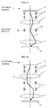
- Fig. 12 shows an example of trajectory control in a case where the aperture 8 is disposed between the focusing lens 6 and the objective lens 7.
- an aberration necessary for correcting the aberration produced by the objective lens when the primary electron beam 4 is inclined is produced by the focusing lens 5, as in the case of Fig. 11, for it is difficult to correct the aberration in the objective lens 7 using the focusing lens 6.
- Fig. 13 shows an example of trajectory control in a case where the beam is inclined while correcting for aberrations in an optical system in which the beam is once focused between lenses disposed in two stages.
- the aperture 8 is disposed between the focusing lens 5 and the electron source.
- the beam is deflected by the aberration control coil 52 composed of deflectors disposed in two stages between the aperture 8 and the focusing lens 5 such that the position of the electron source is apparently at the point of deflection.
- the beam inclination angle control coil 51 is disposed at the point of focus of the beam by the focusing lens 5, so that the angle of inclination of the beam on the sample 10 can be controlled by the beam inclination angle control coil 51.
- Fig. 14 shows an example of trajectory control in a case where the beam is inclined while correcting for aberrations in an optical system in which the beam is not focused between lenses disposed in two stages.
- the direction of aberration produced by the focusing lens 5 is not reversed. Accordingly, the direction of deflection by the beam inclination angle control coil 51 is reversed with respect to that by the aberration control coil 52 so that the aberration by the focusing lens 5 and that by the objective lens 7 can cancel each other out.
- Fig. 15 shows an embodiment in which the aperture 8 is disposed between the focusing lens 5 and the objective lens 7, as opposed to the optical system of Fig. 14 (in which no crossover is crested along the optical axis).
- the beam inclination angle control coil 51 is disposed on either side of the aperture 8 and is operated in a manner such that the trajectory of the deflected primary electron beam 4 passes through the center of the opening of the aperture 8.
- Fig. 16 shows an example of trajectory control in a case where the primary electron beam 4 is inclined by the objective lens 7 while a negative voltage (Vr) is applied to the sample 10.
- Vr negative voltage
- the primary electron beam 4 rapidly decelerates immediately before reaching the sample 10.
- the angle of inclination of the beam on the sample can be increased as compared with a case where no negative voltage is applied.
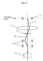
- Fig. 17 shows an embodiment in which a thin film sample 10 is irradiated with the primary electron beam 4 inclined by the objective lens 7, and in which electrons 121 that passed through the sample 10 are detected.
- a scanning transmission image STEM image
- crystal orientation of a sample varies depending on how the thin film slice is cut, crystal orientation errors of the order of several to ten degrees result. Therefore, the primary electron beam is arbitrarily inclined in the present embodiment while preventing the reduction in resolution.
- a deflector 54 is disposed downstream of the thin film sample 10 for aligning the transmitted electrons 121 with respect to a transmitted electron detector 131.
- the deflector 54 is controlled in accordance with the angle of inclination of the primary electron beam 4.
- a means such as a lens or an aperture (not shown) may be disposed between the thin film sample 10 and the transmitted electron detector 131 for limiting the angle of detection of the transmitted electrons.
- Fig. 18 shows an example of trajectory control in the case where two focusing lenses 6a and 6b are disposed between the aperture 8 and the objective lens 7.
- a focusing point of the primary electron beam 4 is located between the focusing lenses 6a and 6b.
- An aberration control coil 52 is disposed at the focusing point so that an aberration is produced by the focusing lens 6b.
- a beam inclination angle control coil 51 is disposed at the point of focus of the primary electron beam by the focusing lens 6b, so that the primary electron beam 4 can be incident on the objective lens 7 off the axis thereof and be inclined with respect to the optical axis.
- the aberration control coil 52 is controlled such that the aberration produced by the objective lens 7 can be cancelled by the aberration in the focusing lens 6b.
- Figs. 19 to 25 show an embodiment in which an aperture transport mechanism is employed as the optical axis control means for controlling the incident position for a plurality of groups of lenses for focusing the charged particle beam.
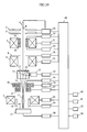
- Fig. 19 shows in particular the overall structure of the scanning electron microscope for measuring the size of a pattern formed on a semiconductor wafer as well as observing the shape thereof. In the following, parts different from the structure depicted in Fig. 1 will be described.
- An astigmatism correction coil 53 and an aligner coil 55 for correcting the irradiated position error produced by the operation of the astigmatism correction coil 53 are disposed at substantially the same height as a first focusing lens 5.
- the coils 53 and 55 are connected via power supplies 33 and 35, respectively, to a computer 40.
- An aperture plate 8 can be accurately transported by a drive mechanism 18 in a plane perpendicular to the optical axis.
- the drive mechanism 18 is connected to the computer 40.
- An image shift coil 57 and an alignment coil 56 are disposed in two stages at the same position as the scanning coil 9 and are connected via power supplies 37 and 36, respectively, to the computer 40.
- Scanning electron microscopes for observing semiconductor wafers generally employ primary electron beams of low acceleration of the order of several hundred volts from the viewpoint of preventing damage to the sample.
- a retarding power supply 38 is connected to apply a negative voltage to the sample 10 so that the primary electron beam 4 can be decelerated.
- a boosting power supply 39 is connected to apply a positive high voltage to a boosting electrode 16 so that the primary electron beam can be accelerated in a later stage, thereby reducing the chromatic aberration in the objective lens 7 and achieving high resolution.
- the retarding and boosting voltages create an electromagnetic field distribution near the surface of the sample 10 whereby the secondary electrons 12 are accelerated towards a reflecting plate (converting electrode) 17.
- the accelerated secondary electrons 12 pass through the scanning coil 9 and collide with the reflecting plate 17, whereby they are converted into new secondary electrons 65.
- the converted secondary electrons 65 are detected by a secondary signal detector 13.
- Fig. 20 shows the trajectory of the primary electron beam 4 in the present embodiment.
- the position of a crossover 4c of the second focusing lens 6 is coincident with that of the aligner coil 56.
- Emitted electrons 4a drawn out of the cathode 1 have a sufficient spread as compared with the aperture size of the aperture plate 8.
- An inclination angle w' t1 of the second focusing lens 6 and the amount ⁇ of shift of the aperture are proportional to one another.
- an inclined image without an off-axis chromatic aberration can be obtained by controlling the beam inclination angle w' t with the aligner coil 56 such that equation (18) is satisfied.
- the feature of the present system namely the aperture transport mechanism, can be realized by simply modifying the manually operated aperture such that it is operated with a computer-controlled drive mechanism. Because the primary electron beam 4b travel off the optical axis in the interval between the cathode 1 and the crossover 4c of the second focusing lens 6, the aberration coefficient of the correction lens becomes several times as large as that of only the second focusing lens. Thus, off-axis chromatic aberrations with inclination angles up to large degrees can be corrected.
- Fig. 21 shows the changes in the correction condition k as the position of the crossover 4c is shifted from the second focusing lens 6 towards the objective lens 7. It is seen that, as the crossover 4c moves closer to the objective lens 7, k decreases until it reaches a point where the off-axis chromatic aberration and the coma aberration can be both corrected simultaneously so that equation (22) can be satisfied.
- Fig. 22 shows the changes in the shift amount ⁇ of the aperture 8 as the position of the crossover 4c is shifted from the second focusing lens 6 towards the objective lens 7 under the condition of equation (18) in which the off-axis chromatic aberration is corrected. It will be seen that, as the crossover 4c is brought closer to the objective lens 7, the shift amount ⁇ decreases.
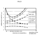
- Fig. 23 shows the changes in the amount of each aberration and the final beam size (or resolution) as the position of the crossover 4c is shifted from the second focusing lens towards the objective lens under the condition of equation (18) in which the off-axis chromatic aberration is corrected.
- the crossover 4c is moved towards the objective lens, the coma aberration decreases, but the diffraction aberration and the image of the electron source size (ratio of reduction of the electron source tip size by the lens) increase, whereby the optimum position of the crossover 4c is determined.
- Fig. 24 shows an embodiment in which the position of the crossover 4c is not made coincident with that of the aligner coil 56, thereby giving priority to resolution.
- a virtual object point 4d as seen from the objective lens 7 does not coincide with the crossover 4c, resulting in a displacement of a point 4e of arrival of the beam on the sample 10 from the central axis.
- This shift can be brought back to the central axis by controlling an image shift coil 57.
- a sample stage 15 may be moved to avoid the field of view error.
- the relationship concerning the beam inclination angle can be preset by registering it in the storage unit 41, for example, so that the position error can be controlled by the computer 40.
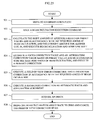
- Fig. 25 shows a flowchart of the process of inclining the beam, including the step of correcting the field of view error.
- S21 an observation point is reached.
- the shift amount of the aperture 8 and the amount of current to be supplied to the aligner coil 56 are calculated from preset values, in accordance with the required angle of beam inclination.
- the beam is then inclined and the aperture is shifted in S23.
- a focus correction value and an astigmatism correction value are estimated from preset values in accordance with the required angle of beam inclination, and a primary correction is performed in S24. This is followed by a field of view error correction and a distortion correction in S25 in accordance with the required beam inclination angle.
- a secondary correction can be completed in S26 within a narrower range of search than that for the normal automatic focus/astigmatism correction.
- an image with high resolution can be obtained in S27.
- the beam inclination angle is brought back to zero, and the field of view error correction in step S25 is cancelled in S28.
Landscapes
- Chemical & Material Sciences (AREA)
- Analytical Chemistry (AREA)
- Electron Beam Exposure (AREA)
- Electron Sources, Ion Sources (AREA)
Abstract
Description
- Δwi :
- Aberration on the image surface
- w'i :
- Inclination of trajectory towards the image surface
- w'i :
- Complex conjugate of w ' / i
- Csi:
- Spherical aberration coefficient on the image surface
- Cci:
- On-axis chromatic aberration coefficient on the image surface
- ΔV:
- Variations in beam energy
- Vi :
- Beam energy on the image surface


Claims (12)
- A charged particle beam apparatus comprising a charged particle source (1) and an optical system for focusing a beam (4) of charged particles emitted by said source and scanning a sample (10) with the focused beam, said apparatus further comprising:optical axis control means for controlling the incident point of the beam (4) on at least two stages of focusing lenses (5, 6, 7) including an objective lens (7), wherein the incident position of the beam is controlled by said optical axis control means such that an off-axis chromatic aberration produced by the objective lens and that produced by other lenses cancel each other out.
- A charged particle beam apparatus comprising a charged particle source (1) and an optical system for focusing a beam (4) of charged particles emitted by said source and scanning a sample (10) with the focused beam, said apparatus further comprising:optical axis control means for controlling the incident point of the beam (4) on at least two stages of focusing lenses (5, 6, 7) including an objective lens (7), wherein the incident position of the beam is controlled by said optical axis control means such that a coma aberration produced by the objective lens and that produced by other lenses cancel each other out.
- A charged particle beam apparatus comprising a charged particle source (1) and an optical system for focusing a beam (4) of charged particles emitted by said source and scanning a sample (10) with the focused beam, said apparatus further comprising:wherein the focusing lenses (5, 6, 7) are controlled by the lens control means and the incident position of the beam (4) is controlled by the optical axis control means such that an off-axis chromatic aberration and a coma aberration produced by the objective lens (7) and the other lenses cancel each other out.optical axis control means for controlling the incident point of the beam (4) on at least two stages of focusing lenses (5, 6, 7) including an objective lens (7); andlens control means for independently controlling a plurality of said focusing lenses (5, 6, 7) ,
- The apparatus of any preceding claim,
wherein the focusing lenses (5, 6) other than the objective lens (7) include a first lens (5) and a second lens (6), the first lens having magnetic poles with a relatively large opening diameter and gap, and the second lens having magnetic poles with a relatively small opening diameter and gap, and
wherein the first lens (5) is excited when the beam (4) is shone on the sample (10) under observation parallel to the optical axis while turning off the first lens, and the second lens (6) is excited when the beam is shone on the sample at an angle with respect to the optical axis while turning off the first lens. - The apparatus of any one of claims 1 to 3, wherein the optical axis control means comprises an aperture (8) and a transport mechanism for moving the aperture in a plane perpendicular to the optical axis.
- A charged particle beam apparatus comprising a charged particle source (1) and an optical system for focusing a beam (4) of charged particles emitted by said source and scanning a sample (10) with the focused beam, said apparatus further comprising:a deflector disposed between the source (1) and at least two stages of focusing lenses (5, 6, 7) including an objective lens (7) for deflecting the beam (4) such that the aberration created by the objective lens and that created by the other lenses cancel each other out.
- A charged particle beam apparatus comprising a charged particle source (1) and an optical system for focusing a beam (4) of charged particles emitted by said source and scanning a sample (10) with the focused beam, said apparatus further comprising:an aperture mechanism transportable in a direction perpendicular to the optical axis, said aperture mechanism disposed between the source (1) and at least two stages of focusing lenses (5, 6, 7) including an objective lens (7), wherein the aperture mechanism limits the passage of the beam (4) such that the aberration produced by the objective lens and that produced by the other lenses cancel each other out.
- The apparatus of any preceding claim, wherein the beam (4) is shone on the sample (10) under observation at an angle with respect to the optical axis.
- The apparatus of claim 8, further comprising astigmatism correction means controlled in accordance with the inclination angle of the beam (4).
- The apparatus of claim 8 or 9, wherein the focal length of the objective lens (7) is controlled in accordance with the inclination angle of the beam (4).
- The apparatus of any one of claims 8 to 10, wherein an irradiated position error of the beam (4) on the sample (10) is corrected in accordance with the inclination angle of the beam.
- A method of irradiating a sample (10) with a charged particle beam (4) at an angle with respect to the optical axis, using a charged particle beam apparatus comprising a charged particle beam source (1) and at least two stages of focusing lenses (5, 6, 7) including an objective lens (7) for focusing the beam of charged particles emitted by the source and scanning the sample with the beam, wherein the beam is incident on that one of the at least two stages of focusing lenses which is closer to the source from a direction such that the aberration produced by the inclination of the beam is offset.
Priority Applications (1)
| Application Number | Priority Date | Filing Date | Title |
|---|---|---|---|
| EP08017746.2A EP2023373B1 (en) | 2002-09-11 | 2003-09-10 | Charged particle beam apparatus and irradiation method |
Applications Claiming Priority (4)
| Application Number | Priority Date | Filing Date | Title |
|---|---|---|---|
| JP2002265842 | 2002-09-11 | ||
| JP2002265842 | 2002-09-11 | ||
| JP2003305267A JP3968334B2 (en) | 2002-09-11 | 2003-08-28 | Charged particle beam apparatus and charged particle beam irradiation method |
| JP2003305267 | 2003-08-28 |
Related Child Applications (1)
| Application Number | Title | Priority Date | Filing Date |
|---|---|---|---|
| EP08017746.2A Division EP2023373B1 (en) | 2002-09-11 | 2003-09-10 | Charged particle beam apparatus and irradiation method |
Publications (3)
| Publication Number | Publication Date |
|---|---|
| EP1398818A2 true EP1398818A2 (en) | 2004-03-17 |
| EP1398818A3 EP1398818A3 (en) | 2005-12-07 |
| EP1398818B1 EP1398818B1 (en) | 2008-11-26 |
Family
ID=31890567
Family Applications (2)
| Application Number | Title | Priority Date | Filing Date |
|---|---|---|---|
| EP08017746.2A Expired - Lifetime EP2023373B1 (en) | 2002-09-11 | 2003-09-10 | Charged particle beam apparatus and irradiation method |
| EP03020626A Expired - Lifetime EP1398818B1 (en) | 2002-09-11 | 2003-09-10 | Charged particle beam apparatus and irradiation method |
Family Applications Before (1)
| Application Number | Title | Priority Date | Filing Date |
|---|---|---|---|
| EP08017746.2A Expired - Lifetime EP2023373B1 (en) | 2002-09-11 | 2003-09-10 | Charged particle beam apparatus and irradiation method |
Country Status (4)
| Country | Link |
|---|---|
| US (3) | US6956211B2 (en) |
| EP (2) | EP2023373B1 (en) |
| JP (1) | JP3968334B2 (en) |
| DE (1) | DE60324870D1 (en) |
Cited By (2)
| Publication number | Priority date | Publication date | Assignee | Title |
|---|---|---|---|---|
| US20080179536A1 (en) * | 2004-06-28 | 2008-07-31 | Hitachi High-Technologies Corportion | Changed particle beam emitting device and method for adjusting the optical axis |
| EP1686609A3 (en) * | 2005-01-26 | 2009-01-14 | Canon Kabushiki Kaisha | Aberration measuring apparatus for charged particle beam optical system, charged particle beam lithography machine having the aberration measuring apparatus, and device fabrication method using the apparatus |
Families Citing this family (48)
| Publication number | Priority date | Publication date | Assignee | Title |
|---|---|---|---|---|
| US6787772B2 (en) * | 2000-01-25 | 2004-09-07 | Hitachi, Ltd. | Scanning electron microscope |
| JP4627771B2 (en) * | 2002-09-11 | 2011-02-09 | 株式会社日立ハイテクノロジーズ | Charged particle beam equipment |
| JP3968334B2 (en) * | 2002-09-11 | 2007-08-29 | 株式会社日立ハイテクノロジーズ | Charged particle beam apparatus and charged particle beam irradiation method |
| JP4383950B2 (en) * | 2004-04-23 | 2009-12-16 | 株式会社日立ハイテクノロジーズ | Charged particle beam adjustment method and charged particle beam apparatus |
| JP4620981B2 (en) | 2004-08-10 | 2011-01-26 | 株式会社日立ハイテクノロジーズ | Charged particle beam equipment |
| JP4310250B2 (en) * | 2004-08-30 | 2009-08-05 | 株式会社日立ハイテクノロジーズ | Charged particle beam adjustment method and charged particle beam apparatus |
| JP2006302523A (en) * | 2005-04-15 | 2006-11-02 | Jeol Ltd | Transmission electron microscope with scanning image observation function |
| EP1929504A4 (en) * | 2005-08-18 | 2009-12-02 | Cebt Co Ltd | Method for changing energy of electron beam in electron column |
| EP1783811A3 (en) * | 2005-11-02 | 2008-02-27 | FEI Company | Corrector for the correction of chromatic aberrations in a particle-optical apparatus |
| JP4299293B2 (en) * | 2005-11-17 | 2009-07-22 | 株式会社ニューフレアテクノロジー | Charged beam lithography system |
| JP2007187538A (en) | 2006-01-13 | 2007-07-26 | Hitachi High-Technologies Corp | Charged particle beam apparatus and image acquisition method using the same |
| JP4988216B2 (en) * | 2006-02-03 | 2012-08-01 | 株式会社日立ハイテクノロジーズ | Charged particle beam equipment equipped with an aberration correction device |
| JP2007218711A (en) * | 2006-02-16 | 2007-08-30 | Hitachi High-Technologies Corp | Measuring method of measurement target pattern using electron microscope device |
| US8026491B2 (en) * | 2006-03-08 | 2011-09-27 | Hitachi High-Technologies Corporation | Charged particle beam apparatus and method for charged particle beam adjustment |
| JP4881661B2 (en) * | 2006-06-20 | 2012-02-22 | 株式会社日立ハイテクノロジーズ | Charged particle beam equipment |
| JP4789260B2 (en) * | 2006-08-23 | 2011-10-12 | エスアイアイ・ナノテクノロジー株式会社 | Charged particle beam apparatus and aperture axis adjusting method |
| EP1914786A3 (en) | 2006-10-20 | 2010-08-04 | JEOL Ltd. | Charged particle beam system |
| JP4945267B2 (en) * | 2007-02-28 | 2012-06-06 | 株式会社日立ハイテクノロジーズ | electronic microscope |
| JP4945463B2 (en) * | 2008-01-18 | 2012-06-06 | 株式会社日立ハイテクノロジーズ | Charged particle beam equipment |
| EP2128885A1 (en) * | 2008-05-26 | 2009-12-02 | FEI Company | Charged particle source with integrated energy filter |
| JP5302595B2 (en) | 2008-08-06 | 2013-10-02 | 株式会社日立ハイテクノロジーズ | Inclination observation method and observation apparatus |
| JP4431624B2 (en) * | 2008-08-25 | 2010-03-17 | 株式会社日立ハイテクノロジーズ | Charged particle beam adjustment method and charged particle beam apparatus |
| US8478021B2 (en) * | 2009-01-15 | 2013-07-02 | Hitachi High-Technologies Corporation | Charged beam device |
| WO2011013342A1 (en) | 2009-07-27 | 2011-02-03 | 株式会社日立ハイテクノロジーズ | Pattern evaluation method, device therefor, and electron beam device |
| JP2013505575A (en) * | 2009-09-18 | 2013-02-14 | マッパー・リソグラフィー・アイピー・ビー.ブイ. | Charged particle optics system with multiple beams |
| JP2010016007A (en) * | 2009-10-22 | 2010-01-21 | Hitachi High-Technologies Corp | Charged particle beam adjustment method, and charged particle beam device |
| EP2325862A1 (en) | 2009-11-18 | 2011-05-25 | Fei Company | Corrector for axial aberrations of a particle-optical lens |
| JP5378185B2 (en) * | 2009-12-08 | 2013-12-25 | 株式会社日立ハイテクノロジーズ | Focused ion beam apparatus and focused ion beam processing method |
| EP2378537B1 (en) | 2010-04-19 | 2014-02-12 | ICT Integrated Circuit Testing Gesellschaft für Halbleiterprüftechnik mbH | Method of operating a charged particle beam device |
| EP2385542B1 (en) * | 2010-05-07 | 2013-01-02 | ICT Integrated Circuit Testing Gesellschaft für Halbleiterprüftechnik mbH | Electron beam device with dispersion compensation, and method of operating same |
| JP5792509B2 (en) * | 2010-07-05 | 2015-10-14 | 株式会社日立ハイテクサイエンス | Charged particle beam apparatus and sample processing method |
| EP2405460B1 (en) * | 2010-07-09 | 2013-02-20 | ICT Integrated Circuit Testing Gesellschaft für Halbleiterprüftechnik mbH | Electron beam device with tilting and dispersion compensation, and method of operating same |
| JP5735262B2 (en) * | 2010-11-12 | 2015-06-17 | 株式会社日立ハイテクノロジーズ | Charged particle optical apparatus and lens aberration measuring method |
| JP5364112B2 (en) * | 2011-01-25 | 2013-12-11 | 株式会社日立ハイテクノロジーズ | Charged particle beam equipment |
| JP5581248B2 (en) * | 2011-03-08 | 2014-08-27 | 株式会社日立ハイテクノロジーズ | Scanning electron microscope |
| EP2511936B1 (en) | 2011-04-13 | 2013-10-02 | Fei Company | Distortion free stigmation of a TEM |
| JP5896870B2 (en) * | 2012-09-21 | 2016-03-30 | 日本電子株式会社 | Scanning electron microscope |
| JP6138454B2 (en) | 2012-10-29 | 2017-05-31 | 株式会社日立ハイテクノロジーズ | Charged particle beam equipment |
| US8921782B2 (en) * | 2012-11-30 | 2014-12-30 | Kla-Tencor Corporation | Tilt-imaging scanning electron microscope |
| US8993980B1 (en) * | 2013-10-22 | 2015-03-31 | Varian Semiconductor Equipment Associates, Inc. | Dual stage scanner for ion beam control |
| US9583306B2 (en) | 2014-12-09 | 2017-02-28 | Hermes Microvision Inc. | Swing objective lens |
| JP6677519B2 (en) * | 2016-02-03 | 2020-04-08 | 日本電子株式会社 | Electron microscope and aberration measurement method |
| US10157727B2 (en) * | 2017-03-02 | 2018-12-18 | Fei Company | Aberration measurement in a charged particle microscope |
| JP2019164886A (en) | 2018-03-19 | 2019-09-26 | 株式会社日立ハイテクノロジーズ | Beam irradiation device |
| TWI744671B (en) * | 2018-08-03 | 2021-11-01 | 日商紐富來科技股份有限公司 | Electron optical system and multi-beam image acquiring apparatus |
| EP3488851A1 (en) | 2018-10-03 | 2019-05-29 | AVM Biotechnology, LLC | Immunoablative therapies |
| JP7292968B2 (en) * | 2019-05-14 | 2023-06-19 | 株式会社ニューフレアテクノロジー | Charged particle beam device |
| US11804357B2 (en) * | 2021-09-30 | 2023-10-31 | Fei Company | Electron optical module for providing an off-axial electron beam with a tunable coma |
Family Cites Families (45)
| Publication number | Priority date | Publication date | Assignee | Title |
|---|---|---|---|---|
| JPS502354B1 (en) * | 1970-12-25 | 1975-01-25 | ||
| JPS502354A (en) | 1973-05-15 | 1975-01-10 | ||
| JPS5176953A (en) | 1974-12-27 | 1976-07-03 | Hitachi Ltd | vfo kairo |
| DD134582A1 (en) * | 1978-01-19 | 1979-03-07 | Eberhard Hahn | METHOD AND DEVICE FOR ADJUSTING AN ELECTRON BEAM PROCESSING SYSTEM |
| JPS5854784Y2 (en) | 1978-09-25 | 1983-12-14 | 株式会社日立製作所 | Stereo scanning electron microscope |
| JPS5548610A (en) | 1978-10-03 | 1980-04-07 | Nakamura Seisakusho:Kk | Dial indicator |
| US4475044A (en) * | 1979-04-23 | 1984-10-02 | Hitachi, Ltd. | Apparatus for focus-deflecting a charged particle beam |
| JPS5628433A (en) * | 1979-08-15 | 1981-03-20 | Erionikusu:Kk | Display distortion corrector for electron beam device |
| JPS57118357A (en) * | 1981-01-14 | 1982-07-23 | Jeol Ltd | Objective lens for scan type electron microscope |
| US4465934A (en) * | 1981-01-23 | 1984-08-14 | Veeco Instruments Inc. | Parallel charged particle beam exposure system |
| JPS5894251A (en) | 1981-11-30 | 1983-06-04 | Fujitsu Ltd | Information transmitting system |
| NL8304217A (en) * | 1983-12-07 | 1985-07-01 | Philips Nv | AUTOMATICALLY ADJUSTABLE ELECTRON MICROSCOPE. |
| JPH0233843A (en) | 1988-07-25 | 1990-02-05 | Hitachi Ltd | Scanning electronic microscope |
| JPH02236936A (en) * | 1989-03-08 | 1990-09-19 | Mitsubishi Electric Corp | Charged beam apparatus |
| NL9100294A (en) * | 1991-02-20 | 1992-09-16 | Philips Nv | LOADED PARTICLE BUNDLE DEVICE. |
| US5369279A (en) * | 1992-06-04 | 1994-11-29 | Martin; Frederick W. | Chromatically compensated particle-beam column |
| JPH06215714A (en) * | 1992-06-05 | 1994-08-05 | Hitachi Ltd | Field emission type transmission electron microscope |
| JP3109785B2 (en) * | 1993-12-21 | 2000-11-20 | 株式会社日立製作所 | Automatic focusing device for scanning electron microscope |
| JPH09129543A (en) * | 1995-11-01 | 1997-05-16 | Nikon Corp | Charged particle beam transfer device |
| US5627373A (en) * | 1996-06-17 | 1997-05-06 | Hewlett-Packard Company | Automatic electron beam alignment and astigmatism correction in scanning electron microscope |
| US6060711A (en) * | 1997-01-27 | 2000-05-09 | Nikon Corporation | Charged-particle optical systems and pattern transfer apparatus comprising same |
| KR19980079377A (en) * | 1997-03-25 | 1998-11-25 | 요시다쇼이치로 | Charged Charity Transfer Device |
| JPH10275581A (en) * | 1997-03-28 | 1998-10-13 | Nikon Corp | Charged particle optics |
| US6064071A (en) * | 1997-04-23 | 2000-05-16 | Nikon Corporation | Charged-particle-beam optical systems |
| JP3754186B2 (en) * | 1997-08-18 | 2006-03-08 | 株式会社トプコン | Electron beam optical device |
| DE19739290A1 (en) * | 1997-09-08 | 1999-03-11 | Ceos Gmbh | Method for eliminating first, second and third order axial image errors by correcting the third order opening error in electron-optical systems |
| EP0999573B1 (en) * | 1998-11-06 | 2006-06-28 | ICT Integrated Circuit Testing Gesellschaft für Halbleiterprüftechnik mbH | Beam column for charged particle device |
| EP1049131B1 (en) | 1999-03-31 | 2008-08-13 | Advantest Corporation | Particle beam apparatus for tilted observation of a specimen |
| US6614026B1 (en) | 1999-04-15 | 2003-09-02 | Applied Materials, Inc. | Charged particle beam column |
| US6452175B1 (en) | 1999-04-15 | 2002-09-17 | Applied Materials, Inc. | Column for charged particle beam device |
| DE19926927A1 (en) * | 1999-06-14 | 2000-12-21 | Ceos Gmbh | Electrostatic corrector to remove the color error from particle lenses |
| US6538249B1 (en) * | 1999-07-09 | 2003-03-25 | Hitachi, Ltd. | Image-formation apparatus using charged particle beams under various focus conditions |
| JP3688160B2 (en) * | 1999-09-17 | 2005-08-24 | 株式会社日立製作所 | Scanning electron microscope |
| WO2001033603A1 (en) | 1999-10-29 | 2001-05-10 | Hitachi, Ltd. | Electron beam apparatus |
| DE60045439D1 (en) * | 2000-01-24 | 2011-02-10 | Integrated Circuit Testing | Bowl for a charged particle beam device |
| EP1150327B1 (en) * | 2000-04-27 | 2018-02-14 | ICT, Integrated Circuit Testing Gesellschaft für Halbleiterprüftechnik mbH | Multi beam charged particle device |
| JP2001357811A (en) * | 2000-06-12 | 2001-12-26 | Hitachi Ltd | Scanning charged particle microscope, focusing method and astigmatism correction method for scanning charged particle microscope |
| DE10044199B9 (en) * | 2000-09-07 | 2005-07-28 | Carl Zeiss Smt Ag | Deflection arrangement and projection system for charged particles |
| DE10109965A1 (en) * | 2001-03-01 | 2002-09-12 | Zeiss Carl | Particle optical lens arrangement and method using such a lens arrangement |
| JP3984019B2 (en) * | 2001-10-15 | 2007-09-26 | パイオニア株式会社 | Electron beam apparatus and electron beam adjusting method |
| JP2003151484A (en) * | 2001-11-15 | 2003-05-23 | Jeol Ltd | Scanning charged particle beam device |
| US7223974B2 (en) * | 2002-05-22 | 2007-05-29 | Applied Materials, Israel, Ltd. | Charged particle beam column and method for directing a charged particle beam |
| US6930308B1 (en) * | 2002-07-11 | 2005-08-16 | Kla-Tencor Technologies Corporation | SEM profile and surface reconstruction using multiple data sets |
| JP3968334B2 (en) * | 2002-09-11 | 2007-08-29 | 株式会社日立ハイテクノロジーズ | Charged particle beam apparatus and charged particle beam irradiation method |
| EP1489641B1 (en) * | 2003-06-18 | 2019-08-14 | ICT Integrated Circuit Testing Gesellschaft für Halbleiterprüftechnik mbH | Charged particle deflecting system |
-
2003
- 2003-08-28 JP JP2003305267A patent/JP3968334B2/en not_active Expired - Fee Related
- 2003-09-08 US US10/656,166 patent/US6956211B2/en not_active Expired - Lifetime
- 2003-09-10 DE DE60324870T patent/DE60324870D1/en not_active Expired - Lifetime
- 2003-09-10 EP EP08017746.2A patent/EP2023373B1/en not_active Expired - Lifetime
- 2003-09-10 EP EP03020626A patent/EP1398818B1/en not_active Expired - Lifetime
-
2005
- 2005-07-21 US US11/185,871 patent/US7282722B2/en not_active Expired - Lifetime
-
2007
- 2007-08-20 US US11/841,411 patent/US7408172B2/en not_active Expired - Lifetime
Cited By (2)
| Publication number | Priority date | Publication date | Assignee | Title |
|---|---|---|---|---|
| US20080179536A1 (en) * | 2004-06-28 | 2008-07-31 | Hitachi High-Technologies Corportion | Changed particle beam emitting device and method for adjusting the optical axis |
| EP1686609A3 (en) * | 2005-01-26 | 2009-01-14 | Canon Kabushiki Kaisha | Aberration measuring apparatus for charged particle beam optical system, charged particle beam lithography machine having the aberration measuring apparatus, and device fabrication method using the apparatus |
Also Published As
| Publication number | Publication date |
|---|---|
| EP1398818B1 (en) | 2008-11-26 |
| EP2023373A2 (en) | 2009-02-11 |
| EP2023373B1 (en) | 2014-04-02 |
| JP2004127930A (en) | 2004-04-22 |
| US20050253083A1 (en) | 2005-11-17 |
| EP2023373A3 (en) | 2012-01-25 |
| US20040119022A1 (en) | 2004-06-24 |
| US7408172B2 (en) | 2008-08-05 |
| DE60324870D1 (en) | 2009-01-08 |
| JP3968334B2 (en) | 2007-08-29 |
| US20080042074A1 (en) | 2008-02-21 |
| EP1398818A3 (en) | 2005-12-07 |
| US7282722B2 (en) | 2007-10-16 |
| US6956211B2 (en) | 2005-10-18 |
Similar Documents
| Publication | Publication Date | Title |
|---|---|---|
| EP2023373B1 (en) | Charged particle beam apparatus and irradiation method | |
| JP4620981B2 (en) | Charged particle beam equipment | |
| US7825377B2 (en) | Electron beam apparatus with aberration corrector | |
| JP5250350B2 (en) | Charged particle beam application equipment | |
| JP4756776B2 (en) | Charged particle beam exposure apparatus, charged particle beam exposure method and device manufacturing method | |
| US6924488B2 (en) | Charged-particle beam apparatus equipped with aberration corrector | |
| US8729491B2 (en) | Charged particle beam apparatus | |
| EP2453463B1 (en) | Method of making axial alignment of charged particle beam and charged particle beam system | |
| US11239042B2 (en) | Beam irradiation device | |
| JP4299195B2 (en) | Charged particle beam apparatus and optical axis adjustment method thereof | |
| US6878937B1 (en) | Prism array for electron beam inspection and defect review | |
| JP2000012438A (en) | Multi-electron beam exposure method and apparatus, and device manufacturing method | |
| JP4627771B2 (en) | Charged particle beam equipment | |
| JP4094042B2 (en) | Charged particle beam apparatus and charged particle beam irradiation method | |
| JP4018197B2 (en) | Electron beam exposure method and electron beam exposure apparatus | |
| JP3772067B2 (en) | Charged particle beam irradiation equipment | |
| JPH10247465A (en) | Scanning charged particle beam device | |
| US20250357067A1 (en) | Aberration corrector for scanning electron microscope with multiple electron beams | |
| JP4995858B2 (en) | Optical axis adjustment method for charged particle beam apparatus | |
| CN116745880A (en) | Electron optics array and methods of directing the primary electron beam onto the sample | |
| JP2000100691A (en) | Electron beam exposure equipment |
Legal Events
| Date | Code | Title | Description |
|---|---|---|---|
| PUAI | Public reference made under article 153(3) epc to a published international application that has entered the european phase |
Free format text: ORIGINAL CODE: 0009012 |
|
| AK | Designated contracting states |
Kind code of ref document: A2 Designated state(s): AT BE BG CH CY CZ DE DK EE ES FI FR GB GR HU IE IT LI LU MC NL PT RO SE SI SK TR |
|
| AX | Request for extension of the european patent |
Extension state: AL LT LV MK |
|
| PUAL | Search report despatched |
Free format text: ORIGINAL CODE: 0009013 |
|
| AK | Designated contracting states |
Kind code of ref document: A3 Designated state(s): AT BE BG CH CY CZ DE DK EE ES FI FR GB GR HU IE IT LI LU MC NL PT RO SE SI SK TR |
|
| AX | Request for extension of the european patent |
Extension state: AL LT LV MK |
|
| 17P | Request for examination filed |
Effective date: 20060331 |
|
| AKX | Designation fees paid |
Designated state(s): DE NL |
|
| 17Q | First examination report despatched |
Effective date: 20060515 |
|
| GRAP | Despatch of communication of intention to grant a patent |
Free format text: ORIGINAL CODE: EPIDOSNIGR1 |
|
| GRAS | Grant fee paid |
Free format text: ORIGINAL CODE: EPIDOSNIGR3 |
|
| RIN1 | Information on inventor provided before grant (corrected) |
Inventor name: ARAI, NORIAKI Inventor name: EZUMI, MAKOTO Inventor name: SATO, MITSUGU Inventor name: DOI, TAKASHI Inventor name: OSE, YOICHI Inventor name: TODOKORO, HIDEO |
|
| GRAA | (expected) grant |
Free format text: ORIGINAL CODE: 0009210 |
|
| AK | Designated contracting states |
Kind code of ref document: B1 Designated state(s): DE NL |
|
| REF | Corresponds to: |
Ref document number: 60324870 Country of ref document: DE Date of ref document: 20090108 Kind code of ref document: P |
|
| PLBE | No opposition filed within time limit |
Free format text: ORIGINAL CODE: 0009261 |
|
| STAA | Information on the status of an ep patent application or granted ep patent |
Free format text: STATUS: NO OPPOSITION FILED WITHIN TIME LIMIT |
|
| 26N | No opposition filed |
Effective date: 20090827 |
|
| PGFP | Annual fee paid to national office [announced via postgrant information from national office to epo] |
Ref country code: NL Payment date: 20100701 Year of fee payment: 8 |
|
| REG | Reference to a national code |
Ref country code: NL Ref legal event code: V1 Effective date: 20120401 |
|
| PG25 | Lapsed in a contracting state [announced via postgrant information from national office to epo] |
Ref country code: NL Free format text: LAPSE BECAUSE OF NON-PAYMENT OF DUE FEES Effective date: 20120401 |
|
| REG | Reference to a national code |
Ref country code: DE Ref legal event code: R082 Ref document number: 60324870 Country of ref document: DE Representative=s name: STREHL SCHUEBEL-HOPF & PARTNER MBB PATENTANWAE, DE Ref country code: DE Ref legal event code: R081 Ref document number: 60324870 Country of ref document: DE Owner name: HITACHI HIGH-TECH CORPORATION, JP Free format text: FORMER OWNER: HITACHI HIGH-TECHNOLOGIES CORPORATION, TOKYO, JP |
|
| PGFP | Annual fee paid to national office [announced via postgrant information from national office to epo] |
Ref country code: DE Payment date: 20220803 Year of fee payment: 20 |
|
| REG | Reference to a national code |
Ref country code: DE Ref legal event code: R071 Ref document number: 60324870 Country of ref document: DE |