BACKGROUND OF THE INVENTION
The present invention relates to a test circuit for a
memory, and especially, to a test circuit for a memory of
a semiconductor integrated circuit in which a memory and a
logic section are mixedly loaded on one semiconductor chip.
In recent years, various kinds of LSIs in which a
memory is mixedly loaded in a logic section such as an
ASIC and a microprocessor have been proposed. In this kind
of LSI, a normal operation of the memory is controlled by
a signal from the logic section, and for example, when a
read command is issued from the logic section, the memory
outputs a data of a selected address to the logic section.
Similarly, the memory outputs the data of the selected
address to the logic section. In this kind of LSI, since
to conduct a test of the memory through the complicated
logic section is impractical, various exclusive test
circuits for conducting a test of the memory have been
proposed.
Fig. 10 is a view showing an arrangement of a
conventional test circuit for a memory (Refer to a patent
document 1 (JP-P2002-42493A (Fig. 5)).). In Fig. 10, 211
is a memory circuit that is an object of a test of the
memory, and has a plurality of data input terminals DI and
a plurality of data output terminals DO. 212 is an
internal logic circuit having an external input terminal
NI, and 213 and 214 are selectors, respectively, each of
which switches input terminals A and B to each other by
means of a switch control signal from a test mode terminal
TEST.
Next, an operation will be explained. In case of
writing a normal data, by means of a switch control signal
from the test mode terminal TEST, both of the selectors
213 and 214 select the input terminals A. The normal data
is input from the external input terminal NI, and is
written into the memory circuit 211 from the data input
terminal DI via the internal logic circuit 212 and the
selector 213. Also, in case of reading the normal data, it
is output from the data output terminal DO of the memory
circuit 211 to an external output terminal OUT via the
internal logic circuit 212 and the selector 214.
In case of writing a test data, by means of the switch
control signal from the test mode terminal TEST, both of
the selectors 213 and 214 select the input terminals B.
The test data is input from a test input terminal TI, and
is written into the memory circuit 211 from the data input
terminal DI via the selector 213. Also, in case of reading
the test data, it is output from the data output terminal
DO of the memory circuit 211 to the external output
terminal OUT via the selector 214.
In conducting a test of the memory, by means of the
switch control of the selectors 213 and 214, such a
conventional test circuit of the memory can conduct the
test of the memory of a single piece of the memory circuit
211 without involving the internal logic circuit 212.
As a prior art of other test circuit of a memory,
there is one known as a built-in self-test circuit (BIST
circuit). While, in the above-mentioned test circuit of
the memory, all of the generation of a test pattern and
the analysis of an output data are conducted by an
external tester, in the BIST circuit, a test pattern
generator and a test result analyzer are provided, and
only a determination result of the test is output to an
external tester. Accordingly, in the BIST circuit, there
is a merit that the number of terminals for the test,
which are necessary for an LSI, requires a small number.
However, in the general BIST circuit, a sequencer is
provided inside the memory test circuit, and since the
sequencer controls test contents, the test contents are
fixed, and it is impossible to change the test contents
after a design of the LSI.
Accordingly, as a method of making it possible to
change the test contents even after the design of the LSI,
a programmable BIST circuit is considered. Fig. 11 is an
arrangement view of a programmable BIST circuit that can
be generally considered. To a memory 102 for a RAM test
command, a program data 101 representing algorithm for
generating the test contents is input from an external
input terminal, and is stored therein. When a test mode
setting signal TEST becomes predetermined logic, a RAM
test control circuit 103 is set to a test mode, and
operates in synchronization with a RAM test clock CLK, and
provides an address specification signal 106 to the memory
102 for a RAM test command, and sequentially reads a
program data 107 from the memory 102 for a RAM test
command.
A test pattern generator 110 sequentially generates a
test pattern data 111 corresponding to the program data in
accordance with a control signal 108 output from the RAM
test control circuit 103. The test pattern data 111 is
switched to a signal 115 during a normal operation by
means of a selector 114, and is selected as an input data
to a memory 116 to be tested.
In such a programmable BIST circuit, by changing the
program data being held in the memory for a RAM test
command, it is possible to perform an arbitrary RAM test.
Also, to avoid an area increase due to the RAM test
command memory, a method has been proposed, in which a
scan path register inside an LSI is substituted for the
RAM test command memory (Refer to a patent document 2 (JP-P2001-297598A
(Fig. 1)).).
In the method wherein, by means of conducting the
switch control of the selector, the test of the memory
circuit is conducted without involving the internal logic
circuit, the terminals for a test, which corresponds to
the numbers of the data input terminals and the data
output terminals, are required. Accordingly, in case that
a bit width of a data input or a data output is large or
in case that a plurality of memories is integrated, there
is a defect that a number of terminals for a test are
required, which becomes impractical.
In the general BIST circuit, a sequencer is provided
inside the circuit, and since the sequencer controls test
contents, the test contents are fixed, and it is
impossible to change the test contents after a design of
the LSI. On the other hand, in the BIST circuit as shown
in Fig. 11, the increase of an area due to the
incorporation of the memory for a RAM test command inside
the LSI, and a test of the memory itself for a RAM test
command also become a problem. In the BIST circuit
proposed in the patent document 2, although the increase
of an area due to the addition of the memory for a RAM
test command does not occur, the increase of an area due
to signal lines or the like for drawing a program from the
scan path register inside the LSI, which is used as the
substitution for the memory for a RAM test command, and
the deterioration of a wiring characteristic during layout
become a problem. Also, since these test circuits generate
a test pattern from a program, there is a defect that, in
the RAM test control circuit and the test pattern
generator, a circuit for conducting the decode of a
program, the generation of a control signal of the RAM or
the like is required, and a circuit size becomes larger.
SUMMARY OF THE INVENTION
The present invention was made to solve the above-described
tasks, and the objective thereof is to realize a
test circuit for a memory, in which test contents can be
changed, by means of the addition of minimum external
terminals for a test and circuits.
A test circuit for a memory of the present invention
is constructed so that, in a test circuit which is
incorporated into a semiconductor integrated circuit
together with the memory, the test circuit has a test
signal generating circuit for generating a test signal for
said memory, and a control circuit for conducting control
of said test signal generating circuit, and a test setting
mode and a test execution mode are switched to each other
in accordance with a first control signal input from
outside, and an initial data of the test signal and a
control data for controlling said test signal generating
circuit, which are input to said test signal generating
circuit in said test setting mode, and a control data to
said control circuit are input serially from an identical
terminal.
In the present invention, since it is constructed so
that the test setting mode and the test execution mode are
switched to each other in accordance with the first
control signal input from outside, and the initial data of
the test signal and the control data for controlling said
test signal generating circuit, which are input to said
test signal generating circuit in said test setting mode,
and the control data to said control circuit are input
serially from the identical terminal, it is possible to
change the test contents of the memory by means of a small
number of external terminals.
BRIEF DESCRIPTION OF THE DRAWINGS
This and other objects, features and advantages of the
present invention will become more apparent upon a reading
of the following detailed description and drawings, in
which:
DESCRIPTION OF THE EMBODIMENTS
Hereinafter, referring to drawings, the present
invention will be explained further in detail based on
embodiments of the present inventions.
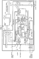
Fig. 1 shows an arrangement of an LSI having a test
circuit for a memory in relation to an embodiment of the
present invention. The LSI to which the test circuit for
the memory of the present invention is applied has a
plurality of RAM 91 - 9m and a test circuit 500.
An output 6 of the test circuit 500 is a data signal,
an address signal, a chip select (CS) signal and a
read/write (R/W) signal that are input signals to each of
the RAM 91 - 9m during a test, and is connected to one of
the inputs of a selector 4, and to the other of the inputs
of the selector 4, the data signal, the address signal,
the CS signal and the R/W signal are connected as an input
signal 7 to each of the RAM 91 - 9m during a normal
operation.
The selector 4 switches the signals 6 and 7 to each
other by means of a test switch signal 1 input from an
external terminal, and an output signal 8 thereof is input
to each of the RAM 91 - 9m. The RAM selected by the CS
signal conducts reading or writing of a data by means of a
value of the R/W signal.
An output from each of the RAM 91 - 9m is also input
to the test circuit 500, and an output data of the RAM
selected by a selector 550 is output to the outside from
the LSI as an output data signal 2.
The test circuit 500 is constructed of the selector 4,
a CS signal generating circuit 510 for generating a CS
signal of the RAM, an address signal generating circuit
520 for generating an address signal of the RAM, a data
signal generating circuit 530 for generating a write data
to the RAM, an R/W signal generating circuit 540 for
generating an R/W signal to the RAM, the selector 550 for
selecting an output signal from the selected RAM by means
of the CS signal, and a test setting control circuit 560
for controlling the values or the like of the CS signal,
the address signal and the data signal of the RAM. Test
control signals 31 - 34 from a control terminal of the LSI
are input to the test setting control circuit 560.
Output signals from the CS signal generating circuit
510, the address signal generating circuit 520, the data
signal generating circuit 530 and the R/W signal
generating circuits 540 that are a test signal generating
circuit of the present invention are output to the
selector 4 as a test signal 6 to each RAM.
The address signal generating circuit 520 has an
Inc/Dec circuit 521 for conducting the increment/decrement
(Inc/Dec) of the address signal to the RAM, and an Inc/Dec
control circuit 522 for controlling it (selecting Inc or
Dec).
The data signal generating circuit 530 has a
reverse/non-reverse circuit 531 for conducting
reverse/non-reverse of the write data to the RAM.
The CS signal generating circuit 510, the address
signal generating circuit 520, the data signal generating
circuit 530 and the test setting control circuit 560 have
shift registers (SR). The Inc/Dec control circuit 522 has
a register (R). The test control signal 31 that becomes a
data for setting a value is input to these SR and R. In
flip-flops constituting these SR and R, a test rest signal
12 to be input from an external terminal is input thereto
in advance, and thereby, an initial value 0 is set.
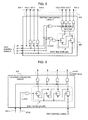
An arrangement example of the test setting control
circuit 560 is shown in Fig. 5. The test setting control
circuit 560 conducts the selection of the SR of the CS
signal generating circuit 510, the SR of the address
signal generating circuit 520, the SR of the data signal
generating circuit 530 and the R of the Inc/Dec control
circuit 522, and the control of the operations of the CS
signal generating circuit 510, the address signal
generating circuit 520, the data signal generating circuit
530 and the R/W signal generating circuits 540.
In Fig. 5, signals 570-5 - 570-8 are selection signals
of the SR of the CS signal generating circuit 510, the SR
of the address signal generating circuit 520, the R of the
Inc/Dec control circuit 522, and the SR of the data signal
generating circuit 530, respectively. The selection
signals 570-5 - 570-8 are generated by decoding a value of
each flip-flop (F/F) constituting the SR in a decoder.
Also, the selection signals 570-5 - 570-8 become active
when the test control signal 34 is 0 and the test control
signal 32 is 1. The setting of the value of this SR is
conducted by giving 0 to the test control signal 34,
giving 1 to the test control signal 33, assuming the test
control signal 31 as a serial input, and latching the
value in synchronization with a clock 11 input from the
external terminal common to other logic section of the LSI.
Signals 570-1 - 570-4 are control signals of the CS signal
generating circuit 510, the address signal generating
circuit 520, the data signal generating circuit 530 and
the R/W signal generating circuit 540, respectively. The
control signals 570-1 - 570-4 become effective when the
test control signal 34 is 1.
An arrangement example of the CS signal generating
circuit 510 is shown in Fig. 6. This figure shows a case
in which there are four RAMs. The CS signal generating
circuit 510 generates a CS signal based on a value of the
F/F constituting the SR of the CS signal generating
circuit 510. The setting of a value of the SR is conducted
by, after setting a value of the SR of the test setting
control circuit 560, giving 0 to the test control signal
34 and giving 1 to the test control signal 32 to make the
selection signal 570-5 active, and assuming the test
control signal 31 as a serial input, and latching the
value in synchronization with the clock 11. A CS signal 6-510
output from the CS signal generating circuit 510 is
output by giving 1 to the test control signal 34 to make
the control signal 570-1 active.
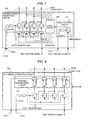
An arrangement example of the address signal
generating circuit 520 is shown in Fig. 7. This figure
shows a case in which an address line has a 4 bit width.
The address signal generating circuit 520 generates an
address signal based on a value of the SR of the address
signal generating circuit 520. The setting of a value of
the SR, which becomes an initial address value, is
conducted by, after setting a value of the SR of the test
setting control circuit 560, giving 0 to the test control
signal 34 and giving 1 to the test control signal 32 to
make the selection signal 570-6 active, and assuming the
test control signal 31 as a serial input, and latching the
value in synchronization with the clock 11. The SR of the
address signal generating circuit 520 has a selector for
making shift-register connection of each F/F constituting
the SR only during a period of time when the selection
signal 570-6 for setting the initial address is active,
and for writing an address signal output from the Inc/Dec
521 into each of these flip-flops in parallel during the
test execution.
The Inc/Dec control circuit 522 generates an Inc/Dec
control signal based on a value of the register (R) of the
Inc/Dec control circuit 522, and based on this value, the
Inc/Dec circuit 521 switches the Inc and Dec to each other.
The setting of a value of the R is conducted by, after
setting a value of the SR of the test setting control
circuit 560, giving 0 to the test control signal 34 and
giving 1 to the test control signal 32 to make the
selection signal 570-7 active, and assuming the test
control signal 31 as a serial input, and latching the
value in synchronization with the clock 11.
In an address signal 6-520 output from the address
signal generating circuit 520, a value of each flip-flop
of the SR is output. The address signal 6-520 is input to
the Inc/Dec circuit 521, and the Inc/Dec circuit 521
conducts the Inc/Dec of the address signal 6-520 and
outputs it. Also, when the control signal 570-2 becomes
active by giving 1 to the test control signal 34 and
giving 1 to the test control signal 33, an output from the
Inc/Dec circuit 521 is written into each flip-flop of the
SR of the address signal generating circuit 520 in
parallel (The Inc/Dec of the address signal is conducted.).
When the control signal 570-2 is not active, a value of
the SR of the address signal generating circuit 520 (the
address signal) does not change.
An arrangement example of the data signal generating
circuit 530 is shown in Fig. 8. This figure shows a case
in which a data line has a 4 bit width. The data signal
generating circuit 530 generates a data signal that
becomes a write data to the RAM, based on a value of each
F/F of the SR of the data signal generating circuit 530.
The setting of a value of the SR is conducted by, after
setting a value of the SR of the test setting control
circuit 560, giving 0 to the test control signal 34 and
giving 1 to the test control signal 32 to make the
selection signal 570-8 active, and assuming the test
control signal 31 as a serial input, and latching the
value in synchronization with the clock 11.
The reverse/non-reverse circuit 531 receives the value
of each F/F of the SR of the data signal generating
circuit 530, and outputs a data in which the value of each
F/F of the SR is reversed, when the control signal 570-3
becomes active by giving 1 to the test control signal 34
and giving 1 to the test control signal 32, and outputs a
non-reversed data when the control signal 570-3 is not
active. A data signal 6-530 output from the data signal
generating circuit 530 is an output from the reverse/non-reverse
circuit 531.
An arrangement example of the R/W signal generating
circuit 540 is shown in Fig. 9. This figure shows a case
in which there are four RAMs. The R/W signal generating
circuit 540 makes an output based on an output 6-510 from
the CS signal generating circuit 510. With regard to an
R/W signal 6-540 output from the R/W signal generating
circuit 540, 1 (write) is output by giving 1 to the test
control signal 34 and giving 1 to the test control signal
31 to make the control signal 570-4 active, and 0 (read)
is output when the control signal 570-4 is not active.
Next, an operation of this embodiment will be
explained. The operation of the test circuit 500 is broken
down into two of a "test setting" and "test execution".
The switching of the "test setting" and the "test
execution" is conducted by the test control signal 34.
First, an operation of the "test setting" will be
explained. The operation of the "test setting" is to
perform the selection of the RAM to be tested (the
determination of a value of CS), the determination of a
test start address value, the selection of the Inc or the
Dec of an address value, and the determination of a value
of a write data. Since the CS signal, the address signal,
the selection of the Inc or Dec of the address, and the
data signal are generated by means of values of the SR
(shift registers) or the R (register) of the CS signal
generating circuit 510, the address signal generating
circuit 520, the Inc/Dec control circuit 522 and the data
signal generating circuit 530, it is work in the "test
setting" to set up the values of these SR or R.
A flow of the "test setting" will be shown below. 1. 0
is given to the test control signal 34. 2. 1 is given to
the test control signal 33, and the value of the SR of the
test control circuit 560 is set by assuming the test
control signal 31 as a serial input, and the SR or R (Here,
the SR of the CS signal generating circuit 510, the
address signal generating circuit 520 and the data signal
generating circuit 530, and the R of the Inc/Dec control
circuit 522) to be set is selected. 3. 1 is given to the
test control signal 32, and the value of the SR or R
selected in 2. is set by assuming the test control signal
31 as a serial input. 4. 2. and 3. are repeated until all
of the values of the SR or R are set.
Next, an operation of the "test execution" will be
explained. The operation of the "test execution" is to
read/write (R/W) a data to the RAM. The presence of the
Inc (Dec) of an address and the presence of R/W or a data
reverse can be controlled in the "test execution".
When 1 is given to the test control signal 33, the Inc
(Dec) of the value of the SR of the address generating
circuit 520 is conducted, and when 0 is given, the Inc
(Dec) is not conducted. The selection of the Inc or Dec is
set in the R of the Inc/Dec control circuit 522 during the
"test setting". When 1 is given to the test control signal
32, the writing to the RAM is conducted, and when 0 is
given, the reading is conducted. When 1 is given to the
test control signal 31, the reverse of the value of the SR
of the data signal generating circuit 530 is conducted,
and when 0 is given, it is not conducted.
A summary of the operation of the test circuit by
means of a combination of the test control signals is
shown in Fig. 2. An example of the operation in accordance
with the operation contents shown in Fig. 2 will be
mentioned below.
First, an example of the operation of the "test
setting" is shown in Fig. 3. By giving 0 to the test
control signal 34, the "test setting" is established. At
time 0, the SR of the test setting control circuit 560
selects (CS) the SR of the CS signal generating circuit.
Here, when 1 is given to the test control signal 32, the
value of the test control signal 31 is input to the SR of
the CS signal generating circuit 510 by means of a serial
input, and the value is set (The RAM 91 is selected.).
At time 1, when 1 is given to the test control signal
33, the value of the test control signal 31 is input to
the SR of the test setting control circuit 560 by means of
a serial input, and the value is set (Inc/Dec). At time 2,
when 1 is given to the test control signal 32, the value
of the test control signal 31 is input to the R of the
Inc/Dec control circuit 522, and the value is set (Dec is
selected.).
In the same manner, values 1, 0 and 1 of the test
control signal 31 during rise of the clock 11 at time 5, 6
and 7 are input to the SR of the data signal generating
circuit 530, and 5 (hexa-decimal) is set, and values 1, 1
and 0 of the test control signal 31 during rise of the
clock 11 at time 10, 11 and 12 are input to the SR of the
address signal generating circuit 520, and 6 (hexa-decimal)
is set. Thereby, the setting is completed.
Next, an example of the operation of the "test
execution" is shown in Fig. 4. By giving 1 to the test
control signal 34, the "test execution" is established,
and a value set in each SR is output as a CS, data or
address signal of the RAM. At time 15, when 1 is given to
the test control signal 32, the R/W signal of the RAM
becomes 1 (W). At time 17, when 1 is given to the test
control signal 31, a value of the data signal of the RAM
becomes a reversed value A (hexa-decimal). At time 18 - 24,
when 1 is given to the test control signal 33, an address
of the RAM is decremented.
As explained above, in the test circuit of the present
invention, the test start address and the data to be
written into the RAM can be freely set, and the timing of
the read/write, the reverse of a data or the increment
(decrement) of an address can be also freely operated.
In addition, although the explanation was made based
on the embodiments, the test circuit of the memory of the
present invention is not limited to the arrangements of
the above-described embodiments, and circuits to which
various changes from the arrangements of the above-described
embodiments are applied are also included in the
scope of the present invention. For example, although, in
the embodiments, the explanation was made on the
assumption that both of the number of memories to be
tested and the bit width of the data signal are four,
these numbers can be easily changed to arbitrary number.
The first advantage is that it is possible to change
the test contents of the RAM by means of a small number of
the external terminals. The reason thereof is that a
serial input is used when a data necessary for the test is
supplied from the outside, and a structure capable of
controlling addressing, timing of R/W or the like from the
external terminals is provided.
The second advantage is that it is possible to
construct the test circuit of the RAM by means of a small
number of hardware. The reason thereof is that it does not
have a sequencer, a ROM code or the like for operating or
determining the contents of the test inside the circuit,
and it has an arrangement capable of operating the test
contents by means of the minimum shift registers and a
small number of logic inside the circuit, and a small
number of the external terminals.