EP1393132B1 - Exposure control for phase shifting photolithographic masks - Google Patents
Exposure control for phase shifting photolithographic masks Download PDFInfo
- Publication number
- EP1393132B1 EP1393132B1 EP02778961A EP02778961A EP1393132B1 EP 1393132 B1 EP1393132 B1 EP 1393132B1 EP 02778961 A EP02778961 A EP 02778961A EP 02778961 A EP02778961 A EP 02778961A EP 1393132 B1 EP1393132 B1 EP 1393132B1
- Authority
- EP
- European Patent Office
- Prior art keywords
- pattern
- mask
- layer
- phase shifting
- phase
- Prior art date
- Legal status (The legal status is an assumption and is not a legal conclusion. Google has not performed a legal analysis and makes no representation as to the accuracy of the status listed.)
- Expired - Lifetime
Links
- 238000004519 manufacturing process Methods 0.000 claims abstract description 15
- 230000010363 phase shift Effects 0.000 claims description 42
- 230000003287 optical effect Effects 0.000 claims description 33
- 238000000034 method Methods 0.000 claims description 31
- 239000000463 material Substances 0.000 claims description 23
- 230000005855 radiation Effects 0.000 claims description 18
- 238000013461 design Methods 0.000 claims description 15
- 238000005286 illumination Methods 0.000 claims description 15
- 230000008569 process Effects 0.000 claims description 11
- 238000000206 photolithography Methods 0.000 claims description 8
- 238000012360 testing method Methods 0.000 claims description 3
- 238000013459 approach Methods 0.000 abstract description 10
- 235000012431 wafers Nutrition 0.000 description 44
- 239000010410 layer Substances 0.000 description 28
- 230000000873 masking effect Effects 0.000 description 7
- 238000004088 simulation Methods 0.000 description 7
- 229920002120 photoresistant polymer Polymers 0.000 description 5
- 230000001427 coherent effect Effects 0.000 description 4
- 229910021420 polycrystalline silicon Inorganic materials 0.000 description 4
- 229920005591 polysilicon Polymers 0.000 description 4
- 239000002253 acid Substances 0.000 description 3
- 238000012545 processing Methods 0.000 description 3
- CURLTUGMZLYLDI-UHFFFAOYSA-N Carbon dioxide Chemical compound O=C=O CURLTUGMZLYLDI-UHFFFAOYSA-N 0.000 description 2
- 230000008859 change Effects 0.000 description 2
- 230000000052 comparative effect Effects 0.000 description 2
- 238000004590 computer program Methods 0.000 description 2
- 230000000694 effects Effects 0.000 description 2
- 238000005516 engineering process Methods 0.000 description 2
- 238000005530 etching Methods 0.000 description 2
- 238000007687 exposure technique Methods 0.000 description 2
- 238000001459 lithography Methods 0.000 description 2
- 238000012986 modification Methods 0.000 description 2
- 230000004048 modification Effects 0.000 description 2
- 239000004065 semiconductor Substances 0.000 description 2
- 238000010420 art technique Methods 0.000 description 1
- 230000015572 biosynthetic process Effects 0.000 description 1
- 239000003990 capacitor Substances 0.000 description 1
- 229910002092 carbon dioxide Inorganic materials 0.000 description 1
- 239000001569 carbon dioxide Substances 0.000 description 1
- 230000000295 complement effect Effects 0.000 description 1
- 230000001419 dependent effect Effects 0.000 description 1
- 230000008021 deposition Effects 0.000 description 1
- 230000009977 dual effect Effects 0.000 description 1
- 238000005259 measurement Methods 0.000 description 1
- 238000001393 microlithography Methods 0.000 description 1
- 229920003259 poly(silylenemethylene) Polymers 0.000 description 1
- 229920000642 polymer Polymers 0.000 description 1
- 238000000926 separation method Methods 0.000 description 1
- 239000002356 single layer Substances 0.000 description 1
- 239000000126 substance Substances 0.000 description 1
Images


Classifications
-
- G—PHYSICS
- G03—PHOTOGRAPHY; CINEMATOGRAPHY; ANALOGOUS TECHNIQUES USING WAVES OTHER THAN OPTICAL WAVES; ELECTROGRAPHY; HOLOGRAPHY
- G03F—PHOTOMECHANICAL PRODUCTION OF TEXTURED OR PATTERNED SURFACES, e.g. FOR PRINTING, FOR PROCESSING OF SEMICONDUCTOR DEVICES; MATERIALS THEREFOR; ORIGINALS THEREFOR; APPARATUS SPECIALLY ADAPTED THEREFOR
- G03F7/00—Photomechanical, e.g. photolithographic, production of textured or patterned surfaces, e.g. printing surfaces; Materials therefor, e.g. comprising photoresists; Apparatus specially adapted therefor
- G03F7/70—Microphotolithographic exposure; Apparatus therefor
- G03F7/70425—Imaging strategies, e.g. for increasing throughput or resolution, printing product fields larger than the image field or compensating lithography- or non-lithography errors, e.g. proximity correction, mix-and-match, stitching or double patterning
- G03F7/70466—Multiple exposures, e.g. combination of fine and coarse exposures, double patterning or multiple exposures for printing a single feature
-
- G—PHYSICS
- G03—PHOTOGRAPHY; CINEMATOGRAPHY; ANALOGOUS TECHNIQUES USING WAVES OTHER THAN OPTICAL WAVES; ELECTROGRAPHY; HOLOGRAPHY
- G03F—PHOTOMECHANICAL PRODUCTION OF TEXTURED OR PATTERNED SURFACES, e.g. FOR PRINTING, FOR PROCESSING OF SEMICONDUCTOR DEVICES; MATERIALS THEREFOR; ORIGINALS THEREFOR; APPARATUS SPECIALLY ADAPTED THEREFOR
- G03F1/00—Originals for photomechanical production of textured or patterned surfaces, e.g., masks, photo-masks, reticles; Mask blanks or pellicles therefor; Containers specially adapted therefor; Preparation thereof
- G03F1/26—Phase shift masks [PSM]; PSM blanks; Preparation thereof
-
- G—PHYSICS
- G03—PHOTOGRAPHY; CINEMATOGRAPHY; ANALOGOUS TECHNIQUES USING WAVES OTHER THAN OPTICAL WAVES; ELECTROGRAPHY; HOLOGRAPHY
- G03F—PHOTOMECHANICAL PRODUCTION OF TEXTURED OR PATTERNED SURFACES, e.g. FOR PRINTING, FOR PROCESSING OF SEMICONDUCTOR DEVICES; MATERIALS THEREFOR; ORIGINALS THEREFOR; APPARATUS SPECIALLY ADAPTED THEREFOR
- G03F1/00—Originals for photomechanical production of textured or patterned surfaces, e.g., masks, photo-masks, reticles; Mask blanks or pellicles therefor; Containers specially adapted therefor; Preparation thereof
- G03F1/68—Preparation processes not covered by groups G03F1/20 - G03F1/50
- G03F1/70—Adapting basic layout or design of masks to lithographic process requirements, e.g., second iteration correction of mask patterns for imaging
-
- G—PHYSICS
- G03—PHOTOGRAPHY; CINEMATOGRAPHY; ANALOGOUS TECHNIQUES USING WAVES OTHER THAN OPTICAL WAVES; ELECTROGRAPHY; HOLOGRAPHY
- G03F—PHOTOMECHANICAL PRODUCTION OF TEXTURED OR PATTERNED SURFACES, e.g. FOR PRINTING, FOR PROCESSING OF SEMICONDUCTOR DEVICES; MATERIALS THEREFOR; ORIGINALS THEREFOR; APPARATUS SPECIALLY ADAPTED THEREFOR
- G03F7/00—Photomechanical, e.g. photolithographic, production of textured or patterned surfaces, e.g. printing surfaces; Materials therefor, e.g. comprising photoresists; Apparatus specially adapted therefor
- G03F7/70—Microphotolithographic exposure; Apparatus therefor
- G03F7/70425—Imaging strategies, e.g. for increasing throughput or resolution, printing product fields larger than the image field or compensating lithography- or non-lithography errors, e.g. proximity correction, mix-and-match, stitching or double patterning
- G03F7/70433—Layout for increasing efficiency or for compensating imaging errors, e.g. layout of exposure fields for reducing focus errors; Use of mask features for increasing efficiency or for compensating imaging errors
-
- G—PHYSICS
- G03—PHOTOGRAPHY; CINEMATOGRAPHY; ANALOGOUS TECHNIQUES USING WAVES OTHER THAN OPTICAL WAVES; ELECTROGRAPHY; HOLOGRAPHY
- G03F—PHOTOMECHANICAL PRODUCTION OF TEXTURED OR PATTERNED SURFACES, e.g. FOR PRINTING, FOR PROCESSING OF SEMICONDUCTOR DEVICES; MATERIALS THEREFOR; ORIGINALS THEREFOR; APPARATUS SPECIALLY ADAPTED THEREFOR
- G03F7/00—Photomechanical, e.g. photolithographic, production of textured or patterned surfaces, e.g. printing surfaces; Materials therefor, e.g. comprising photoresists; Apparatus specially adapted therefor
- G03F7/70—Microphotolithographic exposure; Apparatus therefor
- G03F7/70483—Information management; Active and passive control; Testing; Wafer monitoring, e.g. pattern monitoring
- G03F7/7055—Exposure light control in all parts of the microlithographic apparatus, e.g. pulse length control or light interruption
- G03F7/70558—Dose control, i.e. achievement of a desired dose
Definitions
- the present invention relates to manufacturing small dimension features of objects, such as integrated circuits, using photolithographic masks. More particularly, the present invention relates to the application of phase shift masking to complex layouts for integrated circuits and similar objects.
- Phase shift masking has been applied to create small dimension features in integrated circuits. Typically the features have been limited to selected elements of the design, which have a small, critical dimension. See, for example, United States Patent No. 5,766,806 .
- phase shift masking is a location in the layout at which two phase shift windows having the same phase are laid out in proximity to a feature to be exposed by the masks, such as by overlapping of the phase shift windows intended for implementation of adjacent lines in the exposure pattern. If the phase shift windows have the same phase, then they do not result in the optical interference necessary to create the desired feature. Thus, it is necessary to prevent inadvertent layout of phase shift windows in phase conflict near features to be formed in the layer defined by the mask.
- phase shift masking arises from the need for two different mask patterns for implementation of a layer of material having small dimension features.
- Existing systems expose the wafer using a binary mask pattern using a stepper having optical settings optimized for the binary mask pattern, and expose the wafer using the phase shift mask pattern using a stepper having optical settings optimized for the phase shift mask pattern.
- the optical settings are quite different.
- a phase shift pattern is usually exposed using a highly coherent radiation source.
- binary masks achieve better results having less coherent radiation sources.
- the wafer is required to sit while the settings and masks are changed within the stepper. During the time the wafer sits, the quality of the resist can degrade.
- a “gate shrink” design, or mask is simply a layout, or mask, where significant portions of a pattern, usually field polysilicon, must still print properly using the corresponding binary trim mask, while portions such as transistor gates are formed using phase shifting, resulting in so-called “shrunk” gates.
- phase shifting masks require a low partial coherence ⁇ arrangement in the stepper, so that the light exposing the wafer is highly coherent.
- the binary trim pattern on a mask for a gate shrink-type design would commonly be exposed using low coherency (high ⁇ ) or off-axis illumination.
- the phase shifting pattern on a mask for such a gate shrink-type design would use high coherency (low ⁇ ) illumination. This requires an adjustment of the projection system in the stepper, typically a change in size of an aperture, between the phase shifting pattern and trim pattern exposures.
- US-A-5995200 discloses a mask or reticle on which is formed multiple integrated circuit mask patterns spaced in rows and columns in a rectangular array.
- the masks patterns may be phase shift (i.e. reflective) mask patterns or trim (i.e. refractive) mask patterns, wherein the phase shift mask pattern and trim mask patterns may be complimentary to fabricate a single layer of an integrated circuit.
- the optical settings of a stepper are maintained constant except for dosing between exposure with the phase shifting pattern and the binary trim pattern.
- Optical settings that are not changed between the exposures of the phase shifting and trim patterns include one or more members of a set of optical parameters including numerical aperture (N.A.), wavelength ([lambda]) of light, coherency (such as measured by partial coherence [sigma]), illumination configuration (single spot source, dipole source, quadrapole source, annular source), axis of illumination, and defocus, in various combinations.
- r is determined from simulation results for a particular optical lithography model, e.g. stepper, wavelength, resist measurements, etc.
- both patterns are provided on a single reticle in one embodiment of the present invention.
- a single reticle with multiple patterns can increase mask manufacturing costs. However, the cost of the mask is justified because the use of the single reticle can improve yield, and save manufacturing steps and time.
- a multiple pattern reticle can allow more rapid exposure of the layer of material using both the phase shifting pattern and the trim pattern.
- the layout of patterns on the single reticle can be simple (one of each) or more complex (multiple phase patterns; multiple binary patterns; one-dimensional; two-dimensional; etc.)
- the dosing ratio r for a layer to be exposed can be implemented, for example using constant exposure doses to each pattern with the ratio of the number of phase shifting patterns and to the number of trim patterns on the mask set equal to the dosage ratio 1.0: r.
- the exposure dosage is another parameter that is not changed between exposures of the phase shift and trim patterns.
- a method for manufacturing an integrated circuit includes forming a layer of resist on a semiconductor wafer, moving the wafer to a stepper system including a radiation source and a reticle having a phase shifting pattern and a trim pattern; positioning the wafer and the reticle for exposure of a phase shifting pattern in the reticle; applying a dose of radiation to the wafer through the phase shifting pattern using stepper settings including a set of optical parameters including numerical aperture (N.A.), wavelength ([lambda]) of light, coherency (such as measured by partial coherence [sigma]), illumination configuration (single spot source, dipole source, quadrapole source, annular source), axis of illumination, and defocus; positioning the wafer and the reticle for exposure of a trim pattern in the reticle; applying a dose of radiation to the wafer through the trim pattern using stepper settings including said set of parameters for the trim exposure, wherein all or some of the members of said set of parameters are substantially the same as those used for
- phase shifting and trim patterns may be exposed in any order that results in the die on the wafer being exposed using both, and receiving proper dosages of radiation for the phase shifting and trim patterns. After exposing both patterns, the wafer is removed from the stepper, and available for subsequent steps to complete the integrated circuit. Then, the stepper is available for a next wafer in the line.
- all of said stepper settings are the same, in the sense that the stepper settings are not altered, or in other embodiments, settings of parameters that involve changing or moving an optical device such as an aperture stop setting or a lens position are not changed, between the phase shifting and trim exposures.
- one reticle carries the phase shifting pattern and another carries the trim pattern, and the steps of positioning the reticle and the wafer include selecting the appropriate reticle.
- the photoresist is developed, and the resulting pattern of developed photoresist is used for formation of a layer of polysilicon on the wafer, including elements of circuits being formed thereon.
- elements include transistor gates, interconnect structures, and the like.
- Resulting ICs produced according to embodiments of the invention can include a large number of subwavelength features due to the use of phase shifting and those features will tend to be extremely well defmed because of the high quality energy profile achieved, and the ability to rapidly develop the photoresist by using embodiments of the invention (shorter and more uniform time intervals between exposures; fewer mistakes in lithography settings, fewer mistakes in optical settings; etc.)
- Fig. 1 illustrates a pattern of features and phase shift regions for defining those features.
- Fig. 2 illustrates a simulated exposure of the layout of Fig. 1 according to a 1:2 dosage ratio between the phase shifting mask and the trim mask.
- Fig. 3 illustrates a simulated exposure of the layout of Fig. 1 according to a 1:1 dosage ration between the phase shifting mask and the trim mask.
- Fig. 4 illustrates a single reticle having both a phase shifting and trim patterns.
- Fig. 5 illustrates a portion of a wafer after a first exposure by the reticle of Fig. 4 .
- Fig. 6 illustrates the wafer of Fig. 5 after a second exposure by the reticle of Fig. 4 .
- Fig. 7 illustrates a portion of a wafer after a first exposure by the reticle of Fig. 4 with blading.
- Fig. 8 illustrates the wafer of Fig. 7 after a second exposure by the reticle of Fig. 4 with blading.
- Fig. 9 illustrates a single reticle having phase shifting pattern and two trim patterns.
- Fig. 10 illustrates a portion of a wafer after a first exposure by the reticle of Fig. 9 .
- Fig. 11 illustrates a portion of a wafer after a second exposure by the reticle of Fig. 9 .
- Fig. 12 illustrates a portion of a wafer after a third exposure by the reticle of Fig. 9 .
- phase shifting masks For use in conjunction with phase shifting masks that produce substantial portions of a pattern of a layer on an integrated circuit (IC) using phase shifting will be considered.
- relative dosing considerations between the phase shifting pattern exposure and the binary, trim pattern exposure will be considered.
- approaches for using a single reticle in the production of ICs using phase shifting will be considered.
- the terms "mask” and "reticle” are synonyms, generally referring to a device carrying patterns, also called layouts, for photolithographic exposure used in manufacture of semiconductor wafers or other workpieces.
- an optical lithography exposure system has a setting of members of a set of one or more optical parameters that control characteristics of exposures, the settings used to expose the phase shifting pattern and the complementary trim pattern used to produce an IC.
- using phase shifting are unchanged, or otherwise kept substantially the same, except for dosing, between the exposures. This is applied for example when all, or substantially all portions, of a pattern are being defined using a phase shifting pattern on a mask, because there is minimal need to print small features using the trim pattern.
- the trim pattern consists of features that have greater design latitude in exposure settings that do the features formed using the phase shifting pattern, and can be exposed with key optical settings such as one or more members of a set of optical parameters including numerical aperture (N.A.), wavelength ( ⁇ ) of light, coherency (such as measured by partial coherence ⁇ ), illumination configuration (single spot source, dipole source, quadrupole source, annular source), axis of illumination, and defocus, in various combinations.
- N.A. numerical aperture
- ⁇ wavelength
- coherency such as measured by partial coherence ⁇
- illumination configuration single spot source, dipole source, quadrupole source, annular source
- axis of illumination and defocus
- Masks having a phase shift pattern that results in all, or substantially all portions, of a pattern on the layer of material being exposed being defined using the phase shifting pattern are sometimes referred to as "full phase” masks.
- the masks are defined according to the process described in United States Patent US-A-7083879 .
- a phase shifting mask that produces substantial portions of a pattern of an IC using phase shifting comprises a phase shifting pattern on the mask where substantially all features for a particular layer are defined using phase shifting.
- a phase shifting mask that produces substantial portions of a pattern of an IC using phase shifting comprises a pattern on a mask such that only features that are non-critical for the binary exposure are non-phase shifted.
- a non-critical feature is a feature where there is greater latitude in critical dimension control such that when the non-critical feature is exposed according to the conditions more fully described below the resulting critical dimension variances are acceptable.
- the relevant layout comprises a layout where phase shifting is used to define at least one of:
- the percentages are determined based on the number of edges, or edge segments, within the pattern defined using phase shifting.
- one or more of the numerical aperture (NA) of the radiation exposing the wafer, the coherency setting ( ⁇ ), the illumination configuration (on/off axis, dipole, quadrapole, annular, etc.), and defocus are kept unchanged between the phase shifting and trim exposures.
- all optical settings that require mechanical adjustment of items in the optical path to change, such as an aperture stop setting, or a lens position, are left unchanged between the phase shifting and trim pattern exposures.
- keeping the stepper settings except for dosing unchanged facilitates the use of the single reticle approach described below. In another embodiment, keeping the stepper setting except for dosing unchanged facilitates the use of a single stepper for exposure of both the phase shifting pattern and the corresponding trim pattern, whether such patterns are on the same mask or on separate masks.
- Fig. 1 a pattern of features and phase shift regions for defining those features is shown.
- the phase shifting design shown in Fig. 1 was manually defined.
- the pattern includes the feature 100 and the feature 102. Of interest is the proximity of the end cap of the feature 100 with the top edge of the feature 102.
- the phase shift regions have been defined with the shifter 104, the shifter 106, the shifter 108, and the shifter 110.
- the shifter 106 and the shifter 110 share a single phase, e.g. 0, as do the shifter 104 and the shifter 108, e.g. ⁇ .
- Fig. 2 and Fig. 3 simulation results for the pattern of Fig. 1 are shown with stepper settings maintained constant, but the relative dosing between pattern exposures changed.
- the outputs include black contour lines (contour line 202, contour line 204, contour line 302, and contour line 304) that indicate where the feature 100 and the feature 102 will print.
- black contour lines contour line 202, contour line 204, contour line 302, and contour line 304.
- r in the ratio 1.0:r where r>1.0 are useful in printing ICs when phase shifting masks of the type discussed here are used.
- a 1:3 ratio is used.
- one or more simulations are performed using the actual and/or test layouts to select r for a particular optical/stepper model.
- the selected ratio reflects a balance between "hard” or over exposure for cut regions (necessary and desirable) versus exposure of areas under the trim (undesirable).
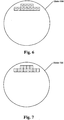
- FIG. 4 illustrates a single reticle having both a phase shifting and trim patterns.
- the reticle 400 includes a phase shifting pattern 402 and a trim pattern 404.
- the phase shifting pattern 402 shows a pattern "1" and the trim pattern 404 a pattern "2" for convenience of explanation of the wafer exposures described below.
- the phase shifting pattern 402 and the trim pattern 404 are separated by a small gap.
- the gap is dependent on the blading capabilities and accuracy for the stepper. In one embodiment, the separation is 5 mm.
- a given stepper/scanner system will have a usable area of a mask, e.g. an n by m millimeter field.
- a usable area of a mask e.g. an n by m millimeter field.
- the number of mask patterns that can be accommodated on a single reticle will depend on the size of the design and the usable reticle area.
- a wafer 500 is shown after the first exposure.
- the wafer 500 has the alternating 1-2 pattern caused by the exposure of some regions to the phase shifting pattern and the exposure of other regions to the trim pattern 404.
- a second exposure, shown in Fig. 6 of the wafer 500 completes the process once the reticle and/or wafer has been repositioned within the stepper.
- Fig. 6 illustrates the pattern as 12 or 21 depending on the order of exposure for a region.
- dosing can be at a user selected ratio, e.g. 1.0: r , between patterns through the use of blading.
- a ratio e.g. 1.0: r
- a second exposure after repositioning the reticle and/or wafer in the stepper is shown in Fig. 8 where the exposure with the phase shifting pattern 402 is complete.
- the blades could then be adjusted to cover the other patterns of the reticle and allow exposures to be made with the trim pattern 404 exposing the wafer.
- Fig. 9 illustrates a single reticle having phase shifting pattern and two trim patterns.
- the reticle 900 includes a phase shifting pattern 902, a trim pattern 904 and a trim pattern 906.
- the trim pattern 904 and the trim pattern 906 are designed to produce the same pattern. Accordingly, by triple exposing the wafer a 1:2 dosing ration between the phase shifting pattern and the trim patterns can be accomplished.
- the results are depicted in Figs. 10-12 showing a portion of the wafer after the first exposure 1000, after the second exposure 1100, and after the third exposure 1200, respectively.
- More complex reticle patterns are possible.
- two phase shifting patterns could be used, e.g. with one phase shifting pattern having structures in one orientation and another pattern with structures in another orientation.
- a two-dimensional pattern of the mask patterns on the reticle is used.
- An embodiment of the present invention also provides method for manufacturing an integrated circuit.
- Method includes forming a layer of resist on a wafer at a first process station.
- the resist is cured and prepared for exposure using a stepper or scanner.
- the wafer with a layer of resist is transported to the stepper.
- the stepper includes a radiation source, a mask and an optical path for exposing the wafer to radiation.
- the optical path is characterized by a set of optical parameters including one or more of a wavelength [lambda] of illumination, numerical aperture NA, coherency, illumination configuration and defocus.
- the layer of resist is exposed to a first dosing radiation to a phase shifting pattern in said mask using a first setting of the set of optical parameters.
- the layer of resist is exposed to a second dose of radiation through the trim pattern in said mask using said first setting.
- the setting of the optical parameters is not changed between the exposures of the phase shift pattern and the trim pattern.
- the mask may have more than one trim pattern and more than one phase shift pattern implemented thereon.
- the wafer may be subject to additional exposure steps, in which the settings of the optical parameters are not changed.
- the order of exposure of the phase shift pattern or patterns and trim pattern or patterns can be changed as suits a particular processing situation.
- both the phase shift and trim exposures are carried out in the same stepper, using the same settings.
- the wafer does not wait for changing of optical parameters, or to be moved from one stepper to the next, between exposures. This reduces the possibility for error in manufacturing of the device, and reduces the time required to complete the exposure step.
- the resist is developed using the techniques that are adapted for use with a particular resist involved.
- a pattern is left on the wafer which is used for a deposition and/or etching step to form of features an integrated circuit.
- the pattern may be used for etching an underlying layer of polysilicon to form interconnect, gate, capacitor, resistor and other circuit features on integrated circuit.
- Maintaining the stepper settings as a constant can significantly improve throughput as well as lead to better critical dimension uniformity. Accordingly, if too much time passes between the first exposure and the second exposure and/or the amount of time is not maintained constant the results may be poorer than expected.
- current generation photoresist materials are chemically amplified so that exposure to light produces a very small number of acid molecules, that then continue to react.
- the passage of time and exposure to air may cause carbon dioxide, and other chemicals, to take up the acid and neutralize it.
- the photoresist should maintain its properties throughout both exposures and the timing between exposures can be shorter and more closely controlled the effect of exposure. Additionally, over time, the acid diffuses into the polymer.
- the increased throughput and yield possible should readily make up for the increase in reticle costs; although, the cost should be comparable, or less than, the cost of a dual reticle approach using separate masks for phase shifting and binary patterns.
- phase shifting can be used to define other layers of material.
- Some examples include computer programs for simulating stepper exposures using phase shift and trim patterns to compute appropriate relative dosing between phase and trim/binary exposures.
- the ICWorkbench(TM) software produced by Numerical Technologies, Inc., San Jose, Calif. is used to simulate the exposure conditions, e.g. as seen in FIGS. 2-3 .
- computer programs are used to develop a pattern of layouts on a single reticle and a corresponding exposure pattern for exposure of wafers by the reticle.
- optical lithography refers processes that include the use of visible, ultraviolet, deep ultraviolet, extreme ultraviolet, x-ray, and other radiation sources for lithography purposes.
Landscapes
- Physics & Mathematics (AREA)
- General Physics & Mathematics (AREA)
- Preparing Plates And Mask In Photomechanical Process (AREA)
- Exposure And Positioning Against Photoresist Photosensitive Materials (AREA)
- Exposure Of Semiconductors, Excluding Electron Or Ion Beam Exposure (AREA)
Applications Claiming Priority (7)
| Application Number | Priority Date | Filing Date | Title |
|---|---|---|---|
| US972428 | 1978-12-22 | ||
| US29678801P | 2001-06-08 | 2001-06-08 | |
| US30414201P | 2001-07-10 | 2001-07-10 | |
| US304142P | 2001-07-10 | ||
| US09/972,428 US6852471B2 (en) | 2001-06-08 | 2001-10-05 | Exposure control for phase shifting photolithographic masks |
| PCT/US2002/018480 WO2002101466A2 (en) | 2001-06-08 | 2002-06-07 | Exposure control for phase shifting photolithographic masks |
| US296788P | 2010-01-20 |
Publications (2)
| Publication Number | Publication Date |
|---|---|
| EP1393132A2 EP1393132A2 (en) | 2004-03-03 |
| EP1393132B1 true EP1393132B1 (en) | 2012-04-25 |
Family
ID=27404462
Family Applications (1)
| Application Number | Title | Priority Date | Filing Date |
|---|---|---|---|
| EP02778961A Expired - Lifetime EP1393132B1 (en) | 2001-06-08 | 2002-06-07 | Exposure control for phase shifting photolithographic masks |
Country Status (7)
| Country | Link |
|---|---|
| US (4) | US6852471B2 (https=) |
| EP (1) | EP1393132B1 (https=) |
| JP (1) | JP2005517282A (https=) |
| CN (1) | CN1282032C (https=) |
| AT (1) | ATE555420T1 (https=) |
| AU (1) | AU2002349203A1 (https=) |
| WO (1) | WO2002101466A2 (https=) |
Families Citing this family (21)
| Publication number | Priority date | Publication date | Assignee | Title |
|---|---|---|---|---|
| US6852471B2 (en) * | 2001-06-08 | 2005-02-08 | Numerical Technologies, Inc. | Exposure control for phase shifting photolithographic masks |
| US6777143B2 (en) * | 2002-01-28 | 2004-08-17 | Taiwan Semiconductor Manufacturing Company | Multiple mask step and scan aligner |
| US7581203B2 (en) * | 2003-06-30 | 2009-08-25 | Agere Systems Inc. | Method and apparatus for manufacturing multiple circuit patterns using a multiple project mask |
| CN100380231C (zh) * | 2003-08-28 | 2008-04-09 | 力晶半导体股份有限公司 | 光学光刻方法 |
| US20050054210A1 (en) * | 2003-09-04 | 2005-03-10 | Taiwan Semiconductor Manufacturing Co., Ltd. | Multiple exposure method for forming patterned photoresist layer |
| US7232630B2 (en) * | 2003-12-11 | 2007-06-19 | Synopsys, Inc | Method for printability enhancement of complementary masks |
| US7448012B1 (en) | 2004-04-21 | 2008-11-04 | Qi-De Qian | Methods and system for improving integrated circuit layout |
| US20080085471A1 (en) * | 2006-10-10 | 2008-04-10 | Anderson Brent A | Photolithographic method using multiple photoexposure apparatus |
| US8431328B2 (en) * | 2007-02-22 | 2013-04-30 | Nikon Corporation | Exposure method, method for manufacturing flat panel display substrate, and exposure apparatus |
| US8071278B1 (en) * | 2007-04-16 | 2011-12-06 | Cadence Design Systems, Inc. | Multiple patterning technique using a single reticle |
| US20080299499A1 (en) * | 2007-05-30 | 2008-12-04 | Naomasa Shiraishi | Exposure method, method of manufacturing plate for flat panel display, and exposure apparatus |
| US7951722B2 (en) | 2007-08-08 | 2011-05-31 | Xilinx, Inc. | Double exposure semiconductor process for improved process margin |
| US7906253B2 (en) * | 2007-09-28 | 2011-03-15 | Texas Instruments Incorporated | System and method for making photomasks |
| US20090311615A1 (en) * | 2008-06-13 | 2009-12-17 | Deming Tang | Method of photolithographic patterning |
| US9005848B2 (en) * | 2008-06-17 | 2015-04-14 | Photronics, Inc. | Photomask having a reduced field size and method of using the same |
| US8479125B2 (en) * | 2009-03-31 | 2013-07-02 | Christophe Pierrat | Lithography modeling and applications |
| US9005849B2 (en) * | 2009-06-17 | 2015-04-14 | Photronics, Inc. | Photomask having a reduced field size and method of using the same |
| US20150221196A1 (en) * | 2012-06-12 | 2015-08-06 | C. Rafin & Co Pty Ltd | Method and Apparatus for Facilitating the Management of Health and Security |
| US20140205934A1 (en) * | 2013-01-21 | 2014-07-24 | Xilinx, Inc. | Single reticle approach for multiple patterning technology |
| CN108319115B (zh) * | 2018-02-28 | 2020-08-21 | 南昌航空大学 | 一种基于虚拟层动态调制的二元数字掩模光刻方法 |
| DE102019121624A1 (de) * | 2018-08-17 | 2020-02-20 | Taiwan Semiconductor Manufacturing Co., Ltd. | Fotolithografieverfahren und -vorrichtung |
Family Cites Families (84)
| Publication number | Priority date | Publication date | Assignee | Title |
|---|---|---|---|---|
| GB1523165A (en) | 1974-08-03 | 1978-08-31 | Matsushita Electric Industrial Co Ltd | Fourier-transform holography by pseudo-random phase shifting |
| US4456371A (en) | 1982-06-30 | 1984-06-26 | International Business Machines Corporation | Optical projection printing threshold leveling arrangement |
| JPH0690505B2 (ja) | 1985-09-20 | 1994-11-14 | 株式会社日立製作所 | ホトマスク |
| JP2710967B2 (ja) | 1988-11-22 | 1998-02-10 | 株式会社日立製作所 | 集積回路装置の製造方法 |
| EP0653679B1 (en) | 1989-04-28 | 2002-08-21 | Fujitsu Limited | Mask, mask producing method and pattern forming method using mask |
| US5328807A (en) | 1990-06-11 | 1994-07-12 | Hitichi, Ltd. | Method of forming a pattern |
| TW198129B (https=) | 1990-06-21 | 1993-01-11 | Matsushita Electron Co Ltd | |
| JP3094439B2 (ja) | 1990-11-21 | 2000-10-03 | 株式会社ニコン | 露光方法 |
| JP2974821B2 (ja) | 1991-06-19 | 1999-11-10 | 沖電気工業株式会社 | パターン形成方法 |
| US5324600A (en) | 1991-07-12 | 1994-06-28 | Oki Electric Industry Co., Ltd. | Method of forming resist pattern and photomask therefor |
| US5364716A (en) | 1991-09-27 | 1994-11-15 | Fujitsu Limited | Pattern exposing method using phase shift and mask used therefor |
| JPH05197128A (ja) | 1991-10-01 | 1993-08-06 | Oki Electric Ind Co Ltd | ホトマスク及びそれを用いたパターン形成方法 |
| US5334542A (en) | 1991-11-27 | 1994-08-02 | Oki Electric Industry Co., Ltd. | Method of forming T-shaped electrode |
| JP3148770B2 (ja) | 1992-03-27 | 2001-03-26 | 日本電信電話株式会社 | ホトマスク及びマスクパタンデータ処理方法 |
| JPH05275303A (ja) * | 1992-03-30 | 1993-10-22 | Hitachi Ltd | 露光方法およびそれに用いるフォトマスク |
| US5308741A (en) | 1992-07-31 | 1994-05-03 | Motorola, Inc. | Lithographic method using double exposure techniques, mask position shifting and light phase shifting |
| US5302477A (en) | 1992-08-21 | 1994-04-12 | Intel Corporation | Inverted phase-shifted reticle |
| US5538815A (en) | 1992-09-14 | 1996-07-23 | Kabushiki Kaisha Toshiba | Method for designing phase-shifting masks with automatization capability |
| US5527645A (en) | 1993-04-21 | 1996-06-18 | Pati; Yagyensh C. | Systematic method for production of phase-shifting photolithographic masks |
| JPH07111528A (ja) | 1993-10-12 | 1995-04-25 | Matsushita Electric Ind Co Ltd | 留守番電話装置 |
| US5424154A (en) * | 1993-12-10 | 1995-06-13 | Intel Corporation | Lithographic emhancement method and apparatus for randomly spaced structures |
| JP3393926B2 (ja) | 1993-12-28 | 2003-04-07 | 株式会社東芝 | フォトマスク設計方法及びその装置 |
| EP0674223B1 (en) | 1994-02-14 | 1997-05-02 | International Business Machines Corporation | An attenuating phase-shift mask structure and fabrication method |
| US5539567A (en) | 1994-06-16 | 1996-07-23 | Texas Instruments Incorporated | Photolithographic technique and illuminator using real-time addressable phase shift light shift |
| US5573890A (en) | 1994-07-18 | 1996-11-12 | Advanced Micro Devices, Inc. | Method of optical lithography using phase shift masking |
| US5538833A (en) | 1994-08-03 | 1996-07-23 | International Business Machines Corporation | High resolution phase edge lithography without the need for a trim mask |
| US5537648A (en) | 1994-08-15 | 1996-07-16 | International Business Machines Corporation | Geometric autogeneration of "hard" phase-shift designs for VLSI |
| US5496666A (en) | 1994-10-27 | 1996-03-05 | Chartered Semiconductor Manufacturing Pte Ltd. | Contact hole mask for semiconductor fabrication |
| US5472814A (en) | 1994-11-17 | 1995-12-05 | International Business Machines Corporation | Orthogonally separated phase shifted and unphase shifted mask patterns for image improvement |
| US5565286A (en) | 1994-11-17 | 1996-10-15 | International Business Machines Corporation | Combined attenuated-alternating phase shifting mask structure and fabrication methods therefor |
| US5523186A (en) | 1994-12-16 | 1996-06-04 | International Business Machines Corporation | Split and cover technique for phase shifting photolithography |
| JP3273456B2 (ja) | 1995-02-24 | 2002-04-08 | アルプス電気株式会社 | モータ駆動スライド型可変抵抗器 |
| US5532090A (en) | 1995-03-01 | 1996-07-02 | Intel Corporation | Method and apparatus for enhanced contact and via lithography |
| US5595843A (en) | 1995-03-30 | 1997-01-21 | Intel Corporation | Layout methodology, mask set, and patterning method for phase-shifting lithography |
| JP2638561B2 (ja) | 1995-05-10 | 1997-08-06 | 株式会社日立製作所 | マスク形成方法 |
| JPH0950951A (ja) * | 1995-08-04 | 1997-02-18 | Nikon Corp | リソグラフィ方法およびリソグラフィ装置 |
| KR0161879B1 (ko) | 1995-09-25 | 1999-01-15 | 문정환 | 위상 반전 마스크의 구조 및 제조방법 |
| JP2917879B2 (ja) | 1995-10-31 | 1999-07-12 | 日本電気株式会社 | フォトマスク及びその製造方法 |
| US6185727B1 (en) | 1995-12-12 | 2001-02-06 | International Business Machines Corporation | Design verification for asymmetric phase shift mask layouts |
| US5885734A (en) | 1996-08-15 | 1999-03-23 | Micron Technology, Inc. | Process for modifying a hierarchical mask layout |
| US5994002A (en) | 1996-09-06 | 1999-11-30 | Matsushita Electric Industrial Co., Ltd. | Photo mask and pattern forming method |
| US5858580A (en) | 1997-09-17 | 1999-01-12 | Numerical Technologies, Inc. | Phase shifting circuit manufacture method and apparatus |
| AU4355397A (en) | 1996-09-18 | 1998-04-14 | Numerical Technologies, Inc. | Phase shifting circuit manufacture method and apparatus |
| US6228539B1 (en) | 1996-09-18 | 2001-05-08 | Numerical Technologies, Inc. | Phase shifting circuit manufacture method and apparatus |
| GB9619839D0 (en) | 1996-09-23 | 1996-11-06 | Hugle Lithography Inc | Photolithography masking arrangements |
| US5923562A (en) | 1996-10-18 | 1999-07-13 | International Business Machines Corporation | Method for automatically eliminating three way intersection design conflicts in phase edge, phase shift designs |
| US5807649A (en) | 1996-10-31 | 1998-09-15 | International Business Machines Corporation | Lithographic patterning method and mask set therefor with light field trim mask |
| JPH10207038A (ja) | 1997-01-28 | 1998-08-07 | Matsushita Electric Ind Co Ltd | レチクル及びパターン形成方法 |
| US5883813A (en) | 1997-03-04 | 1999-03-16 | International Business Machines Corporation | Automatic generation of phase shift masks using net coloring |
| US5923566A (en) | 1997-03-25 | 1999-07-13 | International Business Machines Corporation | Phase shifted design verification routine |
| JP3474740B2 (ja) | 1997-03-25 | 2003-12-08 | 株式会社東芝 | フォトマスクの設計方法 |
| US6057063A (en) | 1997-04-14 | 2000-05-02 | International Business Machines Corporation | Phase shifted mask design system, phase shifted mask and VLSI circuit devices manufactured therewith |
| US6040892A (en) * | 1997-08-19 | 2000-03-21 | Micron Technology, Inc. | Multiple image reticle for forming layers |
| TW363147B (en) | 1997-11-22 | 1999-07-01 | United Microelectronics Corp | Phase shifting mask |
| TW378281B (en) | 1997-11-28 | 2000-01-01 | United Microelectronics Corp | Phase shift mask and method for manufacturing the same |
| US6077630A (en) | 1998-01-08 | 2000-06-20 | Micron Technology, Inc. | Subresolution grating for attenuated phase shifting mask fabrication |
| US6083275A (en) | 1998-01-09 | 2000-07-04 | International Business Machines Corporation | Optimized phase shift design migration |
| JP3307313B2 (ja) | 1998-01-23 | 2002-07-24 | ソニー株式会社 | パターン生成方法及びその装置 |
| WO2000025181A1 (en) | 1998-10-23 | 2000-05-04 | Hitachi, Ltd. | Method for fabricating semiconductor device and method for forming mask suitable therefor |
| US6130012A (en) | 1999-01-13 | 2000-10-10 | Advanced Micro Devices, Inc. | Ion beam milling to generate custom reticles |
| JP4115615B2 (ja) | 1999-03-11 | 2008-07-09 | 株式会社東芝 | マスクパターン設計方法 |
| US6351304B1 (en) * | 1999-06-04 | 2002-02-26 | Canon Kabushiki Kaisha | Multiple exposure method |
| JP3335139B2 (ja) | 1999-06-04 | 2002-10-15 | キヤノン株式会社 | 露光方法、露光装置、およびデバイス製造方法 |
| US6139994A (en) | 1999-06-25 | 2000-10-31 | Broeke; Doug Van Den | Use of intersecting subresolution features for microlithography |
| US6251549B1 (en) | 1999-07-19 | 2001-06-26 | Marc David Levenson | Generic phase shift mask |
| US6335128B1 (en) | 1999-09-28 | 2002-01-01 | Nicolas Bailey Cobb | Method and apparatus for determining phase shifts and trim masks for an integrated circuit |
| US6537867B1 (en) * | 1999-11-03 | 2003-03-25 | Agere Systems Inc. | High speed low voltage semiconductor devices and method of fabrication |
| JP3368265B2 (ja) * | 2000-03-02 | 2003-01-20 | キヤノン株式会社 | 露光方法、露光装置、およびデバイス製造方法 |
| TW512424B (en) | 2000-05-01 | 2002-12-01 | Asml Masktools Bv | Hybrid phase-shift mask |
| US6338922B1 (en) | 2000-05-08 | 2002-01-15 | International Business Machines Corporation | Optimized alternating phase shifted mask design |
| US6787271B2 (en) | 2000-07-05 | 2004-09-07 | Numerical Technologies, Inc. | Design and layout of phase shifting photolithographic masks |
| US7028285B2 (en) | 2000-07-05 | 2006-04-11 | Synopsys, Inc. | Standard cell design incorporating phase information |
| US6733929B2 (en) | 2000-07-05 | 2004-05-11 | Numerical Technologies, Inc. | Phase shift masking for complex patterns with proximity adjustments |
| US6978436B2 (en) | 2000-07-05 | 2005-12-20 | Synopsys, Inc. | Design data format and hierarchy management for phase processing |
| US6681379B2 (en) | 2000-07-05 | 2004-01-20 | Numerical Technologies, Inc. | Phase shifting design and layout for static random access memory |
| US6503666B1 (en) | 2000-07-05 | 2003-01-07 | Numerical Technologies, Inc. | Phase shift masking for complex patterns |
| US6901575B2 (en) | 2000-10-25 | 2005-05-31 | Numerical Technologies, Inc. | Resolving phase-shift conflicts in layouts using weighted links between phase shifters |
| US6628372B2 (en) * | 2001-02-16 | 2003-09-30 | Mccullough Andrew W. | Use of multiple reticles in lithographic printing tools |
| WO2002073312A1 (en) | 2001-03-08 | 2002-09-19 | Numerical Technologies, Inc. | Alternating phase shift masking for multiple levels of masking resolution |
| US6635393B2 (en) | 2001-03-23 | 2003-10-21 | Numerical Technologies, Inc. | Blank for alternating PSM photomask with charge dissipation layer |
| US6566019B2 (en) | 2001-04-03 | 2003-05-20 | Numerical Technologies, Inc. | Using double exposure effects during phase shifting to control line end shortening |
| US6553560B2 (en) | 2001-04-03 | 2003-04-22 | Numerical Technologies, Inc. | Alleviating line end shortening in transistor endcaps by extending phase shifters |
| US6573010B2 (en) | 2001-04-03 | 2003-06-03 | Numerical Technologies, Inc. | Method and apparatus for reducing incidental exposure by using a phase shifter with a variable regulator |
| US6852471B2 (en) * | 2001-06-08 | 2005-02-08 | Numerical Technologies, Inc. | Exposure control for phase shifting photolithographic masks |
-
2001
- 2001-10-05 US US09/972,428 patent/US6852471B2/en not_active Expired - Lifetime
-
2002
- 2002-06-07 EP EP02778961A patent/EP1393132B1/en not_active Expired - Lifetime
- 2002-06-07 AT AT02778961T patent/ATE555420T1/de active
- 2002-06-07 JP JP2003504165A patent/JP2005517282A/ja active Pending
- 2002-06-07 AU AU2002349203A patent/AU2002349203A1/en not_active Abandoned
- 2002-06-07 WO PCT/US2002/018480 patent/WO2002101466A2/en not_active Ceased
- 2002-06-07 CN CNB028115449A patent/CN1282032C/zh not_active Expired - Fee Related
-
2004
- 2004-05-07 US US10/841,276 patent/US7422841B2/en not_active Expired - Lifetime
-
2008
- 2008-04-07 US US12/080,886 patent/US7629109B2/en not_active Expired - Lifetime
-
2009
- 2009-10-16 US US12/589,033 patent/US20100040965A1/en not_active Abandoned
Also Published As
| Publication number | Publication date |
|---|---|
| EP1393132A2 (en) | 2004-03-03 |
| US7422841B2 (en) | 2008-09-09 |
| WO2002101466A3 (en) | 2003-10-09 |
| JP2005517282A (ja) | 2005-06-09 |
| US6852471B2 (en) | 2005-02-08 |
| US20100040965A1 (en) | 2010-02-18 |
| US20040209193A1 (en) | 2004-10-21 |
| US20080187869A1 (en) | 2008-08-07 |
| WO2002101466A2 (en) | 2002-12-19 |
| CN1282032C (zh) | 2006-10-25 |
| AU2002349203A1 (en) | 2002-12-23 |
| CN1514953A (zh) | 2004-07-21 |
| US20020187636A1 (en) | 2002-12-12 |
| US7629109B2 (en) | 2009-12-08 |
| ATE555420T1 (de) | 2012-05-15 |
Similar Documents
| Publication | Publication Date | Title |
|---|---|---|
| US7629109B2 (en) | Exposure control for phase shifting photolithographic masks | |
| US7569309B2 (en) | Gate critical dimension variation by use of ghost features | |
| JP2005517282A6 (ja) | 位相シフトフォトリソグラフィックマスクの露光制御 | |
| US7131102B2 (en) | Full sized scattering bar alt-PSM technique for IC manufacturing in sub-resolution era | |
| US6934007B2 (en) | Method for photolithography using multiple illuminations and a single fine feature mask | |
| US6556277B2 (en) | Photolithographic apparatus | |
| US6472108B1 (en) | Optical proximity correction method | |
| KR100564171B1 (ko) | 포토리소그래피 마스크 및 프로젝션 장치에서의 웨이퍼노출 방법 | |
| EP1472575B1 (en) | Radiation patterning tools, and methods of forming radiation patterning tools | |
| US7859645B2 (en) | Masks and methods of manufacture thereof | |
| US7052808B2 (en) | Transmission mask with differential attenuation to improve ISO-dense proximity | |
| US20020182549A1 (en) | Alternate exposure method for improving photolithography resolution | |
| CN111929981A (zh) | 接触孔光刻工艺热点的光学邻近修正方法 | |
| US6413685B1 (en) | Method of reducing optical proximity effect | |
| US20150010851A1 (en) | Methods involving color-aware retargeting of individual decomposed patterns when designing masks to be used in multiple patterning processes | |
| US6981240B2 (en) | Cutting patterns for full phase shifting masks | |
| US8092958B2 (en) | Mask and method for patterning a semiconductor wafer | |
| US7226707B2 (en) | Methods of printing structures | |
| US20050271949A1 (en) | Reticle manipulations | |
| TW473815B (en) | Method for enhancing lithography resolution |
Legal Events
| Date | Code | Title | Description |
|---|---|---|---|
| PUAI | Public reference made under article 153(3) epc to a published international application that has entered the european phase |
Free format text: ORIGINAL CODE: 0009012 |
|
| 17P | Request for examination filed |
Effective date: 20031217 |
|
| AK | Designated contracting states |
Kind code of ref document: A2 Designated state(s): AT BE CH CY DE DK ES FI FR GB GR IE IT LI LU MC NL PT SE TR |
|
| AX | Request for extension of the european patent |
Extension state: AL LT LV MK RO SI |
|
| RIC1 | Information provided on ipc code assigned before grant |
Ipc: 7G 03F 7/20 B Ipc: 7G 03F 1/00 A Ipc: 7G 03F 1/14 B |
|
| RAP1 | Party data changed (applicant data changed or rights of an application transferred) |
Owner name: SYNOPSYS MERGER HOLDINGS LLC |
|
| RAP1 | Party data changed (applicant data changed or rights of an application transferred) |
Owner name: SYNOPSYS, INC. |
|
| 17Q | First examination report despatched |
Effective date: 20100121 |
|
| GRAP | Despatch of communication of intention to grant a patent |
Free format text: ORIGINAL CODE: EPIDOSNIGR1 |
|
| GRAS | Grant fee paid |
Free format text: ORIGINAL CODE: EPIDOSNIGR3 |
|
| REG | Reference to a national code |
Ref country code: DE Ref legal event code: R079 Ref document number: 60242758 Country of ref document: DE Free format text: PREVIOUS MAIN CLASS: G03F0001000000 Ipc: G03F0001300000 Ref country code: DE Ref legal event code: R079 Ref document number: 60242758 Country of ref document: DE Free format text: PREVIOUS MAIN CLASS: G03F0007000000 Ipc: G03F0001300000 |
|
| GRAA | (expected) grant |
Free format text: ORIGINAL CODE: 0009210 |
|
| RIC1 | Information provided on ipc code assigned before grant |
Ipc: G03F 1/30 20120101AFI20120315BHEP Ipc: G03F 7/20 20060101ALI20120315BHEP |
|
| AK | Designated contracting states |
Kind code of ref document: B1 Designated state(s): AT BE CH CY DE DK ES FI FR GB GR IE IT LI LU MC NL PT SE TR |
|
| REG | Reference to a national code |
Ref country code: GB Ref legal event code: FG4D |
|
| REG | Reference to a national code |
Ref country code: CH Ref legal event code: EP |
|
| REG | Reference to a national code |
Ref country code: AT Ref legal event code: REF Ref document number: 555420 Country of ref document: AT Kind code of ref document: T Effective date: 20120515 |
|
| REG | Reference to a national code |
Ref country code: IE Ref legal event code: FG4D |
|
| REG | Reference to a national code |
Ref country code: DE Ref legal event code: R096 Ref document number: 60242758 Country of ref document: DE Effective date: 20120621 |
|
| REG | Reference to a national code |
Ref country code: NL Ref legal event code: VDEP Effective date: 20120425 |
|
| REG | Reference to a national code |
Ref country code: AT Ref legal event code: MK05 Ref document number: 555420 Country of ref document: AT Kind code of ref document: T Effective date: 20120425 |
|
| PG25 | Lapsed in a contracting state [announced via postgrant information from national office to epo] |
Ref country code: SE Free format text: LAPSE BECAUSE OF FAILURE TO SUBMIT A TRANSLATION OF THE DESCRIPTION OR TO PAY THE FEE WITHIN THE PRESCRIBED TIME-LIMIT Effective date: 20120425 Ref country code: FI Free format text: LAPSE BECAUSE OF FAILURE TO SUBMIT A TRANSLATION OF THE DESCRIPTION OR TO PAY THE FEE WITHIN THE PRESCRIBED TIME-LIMIT Effective date: 20120425 Ref country code: CY Free format text: LAPSE BECAUSE OF FAILURE TO SUBMIT A TRANSLATION OF THE DESCRIPTION OR TO PAY THE FEE WITHIN THE PRESCRIBED TIME-LIMIT Effective date: 20120425 |
|
| PG25 | Lapsed in a contracting state [announced via postgrant information from national office to epo] |
Ref country code: GR Free format text: LAPSE BECAUSE OF FAILURE TO SUBMIT A TRANSLATION OF THE DESCRIPTION OR TO PAY THE FEE WITHIN THE PRESCRIBED TIME-LIMIT Effective date: 20120726 Ref country code: PT Free format text: LAPSE BECAUSE OF FAILURE TO SUBMIT A TRANSLATION OF THE DESCRIPTION OR TO PAY THE FEE WITHIN THE PRESCRIBED TIME-LIMIT Effective date: 20120827 |
|
| PG25 | Lapsed in a contracting state [announced via postgrant information from national office to epo] |
Ref country code: BE Free format text: LAPSE BECAUSE OF FAILURE TO SUBMIT A TRANSLATION OF THE DESCRIPTION OR TO PAY THE FEE WITHIN THE PRESCRIBED TIME-LIMIT Effective date: 20120425 |
|
| PG25 | Lapsed in a contracting state [announced via postgrant information from national office to epo] |
Ref country code: DK Free format text: LAPSE BECAUSE OF FAILURE TO SUBMIT A TRANSLATION OF THE DESCRIPTION OR TO PAY THE FEE WITHIN THE PRESCRIBED TIME-LIMIT Effective date: 20120425 Ref country code: MC Free format text: LAPSE BECAUSE OF NON-PAYMENT OF DUE FEES Effective date: 20120630 Ref country code: NL Free format text: LAPSE BECAUSE OF FAILURE TO SUBMIT A TRANSLATION OF THE DESCRIPTION OR TO PAY THE FEE WITHIN THE PRESCRIBED TIME-LIMIT Effective date: 20120425 Ref country code: AT Free format text: LAPSE BECAUSE OF FAILURE TO SUBMIT A TRANSLATION OF THE DESCRIPTION OR TO PAY THE FEE WITHIN THE PRESCRIBED TIME-LIMIT Effective date: 20120425 |
|
| REG | Reference to a national code |
Ref country code: CH Ref legal event code: PL |
|
| REG | Reference to a national code |
Ref country code: CH Ref legal event code: PL |
|
| PG25 | Lapsed in a contracting state [announced via postgrant information from national office to epo] |
Ref country code: IT Free format text: LAPSE BECAUSE OF FAILURE TO SUBMIT A TRANSLATION OF THE DESCRIPTION OR TO PAY THE FEE WITHIN THE PRESCRIBED TIME-LIMIT Effective date: 20120425 |
|
| PLBE | No opposition filed within time limit |
Free format text: ORIGINAL CODE: 0009261 |
|
| STAA | Information on the status of an ep patent application or granted ep patent |
Free format text: STATUS: NO OPPOSITION FILED WITHIN TIME LIMIT |
|
| REG | Reference to a national code |
Ref country code: IE Ref legal event code: MM4A |
|
| 26N | No opposition filed |
Effective date: 20130128 |
|
| PG25 | Lapsed in a contracting state [announced via postgrant information from national office to epo] |
Ref country code: LI Free format text: LAPSE BECAUSE OF NON-PAYMENT OF DUE FEES Effective date: 20120630 Ref country code: IE Free format text: LAPSE BECAUSE OF NON-PAYMENT OF DUE FEES Effective date: 20120607 Ref country code: ES Free format text: LAPSE BECAUSE OF FAILURE TO SUBMIT A TRANSLATION OF THE DESCRIPTION OR TO PAY THE FEE WITHIN THE PRESCRIBED TIME-LIMIT Effective date: 20120805 Ref country code: CH Free format text: LAPSE BECAUSE OF NON-PAYMENT OF DUE FEES Effective date: 20120630 |
|
| REG | Reference to a national code |
Ref country code: DE Ref legal event code: R097 Ref document number: 60242758 Country of ref document: DE Effective date: 20130128 |
|
| PG25 | Lapsed in a contracting state [announced via postgrant information from national office to epo] |
Ref country code: TR Free format text: LAPSE BECAUSE OF FAILURE TO SUBMIT A TRANSLATION OF THE DESCRIPTION OR TO PAY THE FEE WITHIN THE PRESCRIBED TIME-LIMIT Effective date: 20120425 |
|
| PG25 | Lapsed in a contracting state [announced via postgrant information from national office to epo] |
Ref country code: LU Free format text: LAPSE BECAUSE OF NON-PAYMENT OF DUE FEES Effective date: 20120607 |
|
| REG | Reference to a national code |
Ref country code: FR Ref legal event code: PLFP Year of fee payment: 14 |
|
| PGFP | Annual fee paid to national office [announced via postgrant information from national office to epo] |
Ref country code: GB Payment date: 20150603 Year of fee payment: 14 |
|
| REG | Reference to a national code |
Ref country code: FR Ref legal event code: PLFP Year of fee payment: 15 |
|
| GBPC | Gb: european patent ceased through non-payment of renewal fee |
Effective date: 20160607 |
|
| REG | Reference to a national code |
Ref country code: FR Ref legal event code: PLFP Year of fee payment: 16 |
|
| PG25 | Lapsed in a contracting state [announced via postgrant information from national office to epo] |
Ref country code: GB Free format text: LAPSE BECAUSE OF NON-PAYMENT OF DUE FEES Effective date: 20160607 |
|
| REG | Reference to a national code |
Ref country code: FR Ref legal event code: PLFP Year of fee payment: 17 |
|
| REG | Reference to a national code |
Ref country code: DE Ref legal event code: R082 Ref document number: 60242758 Country of ref document: DE Representative=s name: EPPING HERMANN FISCHER PATENTANWALTSGESELLSCHA, DE |
|
| PGFP | Annual fee paid to national office [announced via postgrant information from national office to epo] |
Ref country code: DE Payment date: 20210519 Year of fee payment: 20 Ref country code: FR Payment date: 20210519 Year of fee payment: 20 |
|
| REG | Reference to a national code |
Ref country code: DE Ref legal event code: R071 Ref document number: 60242758 Country of ref document: DE |