EP1391069B1 - Hinzufügen von signalen in einem mehrwellenlängen-multiplexsystem - Google Patents
Hinzufügen von signalen in einem mehrwellenlängen-multiplexsystem Download PDFInfo
- Publication number
- EP1391069B1 EP1391069B1 EP02711052A EP02711052A EP1391069B1 EP 1391069 B1 EP1391069 B1 EP 1391069B1 EP 02711052 A EP02711052 A EP 02711052A EP 02711052 A EP02711052 A EP 02711052A EP 1391069 B1 EP1391069 B1 EP 1391069B1
- Authority
- EP
- European Patent Office
- Prior art keywords
- signals
- telecommunications system
- wavelength
- added
- bleachable
- Prior art date
- Legal status (The legal status is an assumption and is not a legal conclusion. Google has not performed a legal analysis and makes no representation as to the accuracy of the status listed.)
- Expired - Lifetime
Links
- 230000003287 optical effect Effects 0.000 claims abstract description 49
- 239000000835 fiber Substances 0.000 claims abstract description 24
- 230000005540 biological transmission Effects 0.000 claims abstract description 20
- 239000010410 layer Substances 0.000 claims abstract description 17
- 239000013307 optical fiber Substances 0.000 claims abstract description 7
- 239000004065 semiconductor Substances 0.000 claims abstract description 6
- 238000004061 bleaching Methods 0.000 claims abstract description 4
- 239000002356 single layer Substances 0.000 claims abstract description 3
- GPXJNWSHGFTCBW-UHFFFAOYSA-N Indium phosphide Chemical compound [In]#P GPXJNWSHGFTCBW-UHFFFAOYSA-N 0.000 claims description 11
- 229910000530 Gallium indium arsenide Inorganic materials 0.000 claims description 10
- 230000008878 coupling Effects 0.000 claims description 8
- 238000010168 coupling process Methods 0.000 claims description 8
- 238000005859 coupling reaction Methods 0.000 claims description 8
- 230000002269 spontaneous effect Effects 0.000 claims description 6
- 239000000463 material Substances 0.000 claims description 5
- KXNLCSXBJCPWGL-UHFFFAOYSA-N [Ga].[As].[In] Chemical compound [Ga].[As].[In] KXNLCSXBJCPWGL-UHFFFAOYSA-N 0.000 claims description 4
- UYAHIZSMUZPPFV-UHFFFAOYSA-N erbium Chemical compound [Er] UYAHIZSMUZPPFV-UHFFFAOYSA-N 0.000 claims description 4
- 229910052691 Erbium Inorganic materials 0.000 claims description 3
- 239000011521 glass Substances 0.000 claims description 3
- MARUHZGHZWCEQU-UHFFFAOYSA-N 5-phenyl-2h-tetrazole Chemical compound C1=CC=CC=C1C1=NNN=N1 MARUHZGHZWCEQU-UHFFFAOYSA-N 0.000 claims description 2
- 229910000661 Mercury cadmium telluride Inorganic materials 0.000 claims description 2
- MCMSPRNYOJJPIZ-UHFFFAOYSA-N cadmium;mercury;tellurium Chemical compound [Cd]=[Te]=[Hg] MCMSPRNYOJJPIZ-UHFFFAOYSA-N 0.000 claims description 2
- 238000007725 thermal activation Methods 0.000 claims 2
- 238000004891 communication Methods 0.000 description 6
- 238000000034 method Methods 0.000 description 5
- 239000007844 bleaching agent Substances 0.000 description 4
- 238000003780 insertion Methods 0.000 description 4
- 230000037431 insertion Effects 0.000 description 4
- 238000012545 processing Methods 0.000 description 3
- VYPSYNLAJGMNEJ-UHFFFAOYSA-N Silicium dioxide Chemical compound O=[Si]=O VYPSYNLAJGMNEJ-UHFFFAOYSA-N 0.000 description 2
- 238000010521 absorption reaction Methods 0.000 description 2
- 238000013459 approach Methods 0.000 description 2
- 230000002238 attenuated effect Effects 0.000 description 2
- 230000000903 blocking effect Effects 0.000 description 2
- 238000001914 filtration Methods 0.000 description 2
- 230000002441 reversible effect Effects 0.000 description 2
- 239000000758 substrate Substances 0.000 description 2
- RZVAJINKPMORJF-UHFFFAOYSA-N Acetaminophen Chemical compound CC(=O)NC1=CC=C(O)C=C1 RZVAJINKPMORJF-UHFFFAOYSA-N 0.000 description 1
- XUIMIQQOPSSXEZ-UHFFFAOYSA-N Silicon Chemical compound [Si] XUIMIQQOPSSXEZ-UHFFFAOYSA-N 0.000 description 1
- 239000006096 absorbing agent Substances 0.000 description 1
- 230000003321 amplification Effects 0.000 description 1
- 238000005253 cladding Methods 0.000 description 1
- 230000001427 coherent effect Effects 0.000 description 1
- 239000006185 dispersion Substances 0.000 description 1
- 239000002019 doping agent Substances 0.000 description 1
- 239000000975 dye Substances 0.000 description 1
- 230000007613 environmental effect Effects 0.000 description 1
- 230000002349 favourable effect Effects 0.000 description 1
- 230000002452 interceptive effect Effects 0.000 description 1
- 239000004973 liquid crystal related substance Substances 0.000 description 1
- GQYHUHYESMUTHG-UHFFFAOYSA-N lithium niobate Chemical compound [Li+].[O-][Nb](=O)=O GQYHUHYESMUTHG-UHFFFAOYSA-N 0.000 description 1
- 239000000203 mixture Substances 0.000 description 1
- 238000003199 nucleic acid amplification method Methods 0.000 description 1
- 239000000382 optic material Substances 0.000 description 1
- 238000012856 packing Methods 0.000 description 1
- 230000036961 partial effect Effects 0.000 description 1
- 229920006254 polymer film Polymers 0.000 description 1
- 238000012797 qualification Methods 0.000 description 1
- 230000002829 reductive effect Effects 0.000 description 1
- 238000000926 separation method Methods 0.000 description 1
- 229910052710 silicon Inorganic materials 0.000 description 1
- 239000010703 silicon Substances 0.000 description 1
- 239000000377 silicon dioxide Substances 0.000 description 1
- 230000001629 suppression Effects 0.000 description 1
Images

Classifications
-
- H—ELECTRICITY
- H04—ELECTRIC COMMUNICATION TECHNIQUE
- H04Q—SELECTING
- H04Q11/00—Selecting arrangements for multiplex systems
- H04Q11/0001—Selecting arrangements for multiplex systems using optical switching
- H04Q11/0005—Switch and router aspects
-
- B—PERFORMING OPERATIONS; TRANSPORTING
- B82—NANOTECHNOLOGY
- B82Y—SPECIFIC USES OR APPLICATIONS OF NANOSTRUCTURES; MEASUREMENT OR ANALYSIS OF NANOSTRUCTURES; MANUFACTURE OR TREATMENT OF NANOSTRUCTURES
- B82Y20/00—Nanooptics, e.g. quantum optics or photonic crystals
-
- G—PHYSICS
- G02—OPTICS
- G02B—OPTICAL ELEMENTS, SYSTEMS OR APPARATUS
- G02B26/00—Optical devices or arrangements for the control of light using movable or deformable optical elements
- G02B26/002—Optical devices or arrangements for the control of light using movable or deformable optical elements the movement or the deformation controlling the frequency of light, e.g. by Doppler effect
-
- G—PHYSICS
- G02—OPTICS
- G02B—OPTICAL ELEMENTS, SYSTEMS OR APPARATUS
- G02B6/00—Light guides; Structural details of arrangements comprising light guides and other optical elements, e.g. couplings
- G02B6/24—Coupling light guides
- G02B6/26—Optical coupling means
- G02B6/34—Optical coupling means utilising prism or grating
-
- G—PHYSICS
- G02—OPTICS
- G02F—OPTICAL DEVICES OR ARRANGEMENTS FOR THE CONTROL OF LIGHT BY MODIFICATION OF THE OPTICAL PROPERTIES OF THE MEDIA OF THE ELEMENTS INVOLVED THEREIN; NON-LINEAR OPTICS; FREQUENCY-CHANGING OF LIGHT; OPTICAL LOGIC ELEMENTS; OPTICAL ANALOGUE/DIGITAL CONVERTERS
- G02F1/00—Devices or arrangements for the control of the intensity, colour, phase, polarisation or direction of light arriving from an independent light source, e.g. switching, gating or modulating; Non-linear optics
- G02F1/01—Devices or arrangements for the control of the intensity, colour, phase, polarisation or direction of light arriving from an independent light source, e.g. switching, gating or modulating; Non-linear optics for the control of the intensity, phase, polarisation or colour
- G02F1/015—Devices or arrangements for the control of the intensity, colour, phase, polarisation or direction of light arriving from an independent light source, e.g. switching, gating or modulating; Non-linear optics for the control of the intensity, phase, polarisation or colour based on semiconductor elements having potential barriers, e.g. having a PN or PIN junction
- G02F1/017—Structures with periodic or quasi periodic potential variation, e.g. superlattices, quantum wells
- G02F1/01716—Optically controlled superlattice or quantum well devices
-
- H—ELECTRICITY
- H04—ELECTRIC COMMUNICATION TECHNIQUE
- H04J—MULTIPLEX COMMUNICATION
- H04J14/00—Optical multiplex systems
- H04J14/02—Wavelength-division multiplex systems
- H04J14/0201—Add-and-drop multiplexing
- H04J14/0202—Arrangements therefor
- H04J14/0204—Broadcast and select arrangements, e.g. with an optical splitter at the input before adding or dropping
-
- H—ELECTRICITY
- H04—ELECTRIC COMMUNICATION TECHNIQUE
- H04J—MULTIPLEX COMMUNICATION
- H04J14/00—Optical multiplex systems
- H04J14/02—Wavelength-division multiplex systems
- H04J14/0201—Add-and-drop multiplexing
- H04J14/0202—Arrangements therefor
- H04J14/0205—Select and combine arrangements, e.g. with an optical combiner at the output after adding or dropping
-
- H—ELECTRICITY
- H04—ELECTRIC COMMUNICATION TECHNIQUE
- H04J—MULTIPLEX COMMUNICATION
- H04J14/00—Optical multiplex systems
- H04J14/02—Wavelength-division multiplex systems
- H04J14/0201—Add-and-drop multiplexing
- H04J14/0202—Arrangements therefor
- H04J14/0206—Express channels arrangements
-
- H—ELECTRICITY
- H04—ELECTRIC COMMUNICATION TECHNIQUE
- H04J—MULTIPLEX COMMUNICATION
- H04J14/00—Optical multiplex systems
- H04J14/02—Wavelength-division multiplex systems
- H04J14/0201—Add-and-drop multiplexing
- H04J14/0202—Arrangements therefor
- H04J14/0213—Groups of channels or wave bands arrangements
-
- H—ELECTRICITY
- H04—ELECTRIC COMMUNICATION TECHNIQUE
- H04J—MULTIPLEX COMMUNICATION
- H04J14/00—Optical multiplex systems
- H04J14/02—Wavelength-division multiplex systems
- H04J14/0221—Power control, e.g. to keep the total optical power constant
- H04J14/02216—Power control, e.g. to keep the total optical power constant by gain equalization
-
- G—PHYSICS
- G02—OPTICS
- G02B—OPTICAL ELEMENTS, SYSTEMS OR APPARATUS
- G02B6/00—Light guides; Structural details of arrangements comprising light guides and other optical elements, e.g. couplings
- G02B6/10—Light guides; Structural details of arrangements comprising light guides and other optical elements, e.g. couplings of the optical waveguide type
- G02B6/12—Light guides; Structural details of arrangements comprising light guides and other optical elements, e.g. couplings of the optical waveguide type of the integrated circuit kind
- G02B2006/12133—Functions
- G02B2006/12164—Multiplexing; Demultiplexing
-
- G—PHYSICS
- G02—OPTICS
- G02B—OPTICAL ELEMENTS, SYSTEMS OR APPARATUS
- G02B6/00—Light guides; Structural details of arrangements comprising light guides and other optical elements, e.g. couplings
- G02B6/10—Light guides; Structural details of arrangements comprising light guides and other optical elements, e.g. couplings of the optical waveguide type
- G02B6/12—Light guides; Structural details of arrangements comprising light guides and other optical elements, e.g. couplings of the optical waveguide type of the integrated circuit kind
- G02B6/12007—Light guides; Structural details of arrangements comprising light guides and other optical elements, e.g. couplings of the optical waveguide type of the integrated circuit kind forming wavelength selective elements, e.g. multiplexer, demultiplexer
- G02B6/12009—Light guides; Structural details of arrangements comprising light guides and other optical elements, e.g. couplings of the optical waveguide type of the integrated circuit kind forming wavelength selective elements, e.g. multiplexer, demultiplexer comprising arrayed waveguide grating [AWG] devices, i.e. with a phased array of waveguides
- G02B6/12019—Light guides; Structural details of arrangements comprising light guides and other optical elements, e.g. couplings of the optical waveguide type of the integrated circuit kind forming wavelength selective elements, e.g. multiplexer, demultiplexer comprising arrayed waveguide grating [AWG] devices, i.e. with a phased array of waveguides characterised by the optical interconnection to or from the AWG devices, e.g. integration or coupling with lasers or photodiodes
-
- H—ELECTRICITY
- H04—ELECTRIC COMMUNICATION TECHNIQUE
- H04Q—SELECTING
- H04Q11/00—Selecting arrangements for multiplex systems
- H04Q11/0001—Selecting arrangements for multiplex systems using optical switching
- H04Q11/0005—Switch and router aspects
- H04Q2011/0007—Construction
- H04Q2011/0015—Construction using splitting combining
-
- H—ELECTRICITY
- H04—ELECTRIC COMMUNICATION TECHNIQUE
- H04Q—SELECTING
- H04Q11/00—Selecting arrangements for multiplex systems
- H04Q11/0001—Selecting arrangements for multiplex systems using optical switching
- H04Q11/0005—Switch and router aspects
- H04Q2011/0007—Construction
- H04Q2011/0016—Construction using wavelength multiplexing or demultiplexing
-
- H—ELECTRICITY
- H04—ELECTRIC COMMUNICATION TECHNIQUE
- H04Q—SELECTING
- H04Q11/00—Selecting arrangements for multiplex systems
- H04Q11/0001—Selecting arrangements for multiplex systems using optical switching
- H04Q11/0005—Switch and router aspects
- H04Q2011/0007—Construction
- H04Q2011/0026—Construction using free space propagation (e.g. lenses, mirrors)
-
- H—ELECTRICITY
- H04—ELECTRIC COMMUNICATION TECHNIQUE
- H04Q—SELECTING
- H04Q11/00—Selecting arrangements for multiplex systems
- H04Q11/0001—Selecting arrangements for multiplex systems using optical switching
- H04Q11/0005—Switch and router aspects
- H04Q2011/0007—Construction
- H04Q2011/0035—Construction using miscellaneous components, e.g. circulator, polarisation, acousto/thermo optical
Definitions
- Optical fibres are being operated with many different wavelength channels in wavelength division multiplexed (WDM) systems. These fibres are being used in communications networks in which traffic may be carried on different carrier wavelengths through several switching points. These optical networks may be constructed from optical WDM line systems connected by optical switches and from optical WDM rings interconnected to allow traffic to be selectively switched between rings. A convenient way to construct such rings is from a basic building block at which wavelength traffic channels may be added or dropped from the ring. Such an equipment is called an Optical Add Drop Multiplexer for ring networks. Optical Add Drop Multiplexer functions are also used in WDM line systems to permit a fraction of the WDM channels to be dropped at intermediate points.
- WDM wavelength division multiplexed
- Adding and dropping of wavelength channels to a single mode fibre can be accomplished by means of broadband splitter/combiners such as fibre fused couplers or silica waveguides formed in pairs and run with small dimensional spacing less than a wavelength so that coupling between the optical fields occurs.
- broadband splitter/combiners such as fibre fused couplers or silica waveguides formed in pairs and run with small dimensional spacing less than a wavelength so that coupling between the optical fields occurs.
- splitting/coupling losses are very severe. For example, with two way coupling, loss is more than 50% and for 32 way coupling losses are more than 97%.
- WDM combiners may have n input ports and one output port. To couple into the output port it is necessary to introduce each wavelength channel into its correct port.
- WDM combiners have, in practice, coupling losses between 1dB ( ⁇ 80%) to 7dB ( ⁇ 20%) depending on quality and on band pass characteristics of the filtering of each channel.
- a communications network becomes most economic when it becomes possible to load up all parts of the network and when it is possible to provide alternative 'protection' paths for traffic. This ideal is approached when traffic can be easily switched from one wavelength channel to another and when all switch interconnection options are available, ie when the switches are 'non-blocking'.
- splitter/combiners can be used but then optical amplifiers become necessary to overcome the large losses incurred during the splitter/combiner functions.
- the amplifiers introduce 'noise' due to Amplified Spontaneous Emission (ASE) onto the traffic paths. This manifests as reduced optical signal to noise ratio (OSNR) in the optical signal carrying the communications traffic.
- OSNR optical signal to noise ratio
- US6,278,536 describes an optical transmission device used for bi-directional optical communications.
- Figure 3 of US6,278,536 shows an example of a linear ADM (Add/Drop Multiplexer) unit.
- the ADM includes an acousto-optical tuneable filter (AOTF) for optical signal branching insertion.
- the ADM unit also includes a processing unit for performing specified processing for the optical signals of wavelengths branched by the AOTF.
- the optical signals branched by the AOTF are produced by the processing unit and inserted into optical fibres.
- EP-A-0,948,153 describes an OADM (Optical ADM) including an AOTF.
- the AOTF can select an optional wavelength by changing the frequency of an RF signal to be applied.
- An optical signal having a specified wavelength can be dropped from a wavelength-multiplexed optical signal input from an input terminal, or a wavelength-multiplexed optical signal input from an add port can be multiplexed with a through signal.
- the AOTF should be exclusively used for dropping in an actual device configuration.
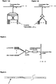
- a telecommunications system comprising a single mode optical fibre carrying Wave Division Multiplex (WDM) traffic and including a transmission fibre coupler arranged to couple signals from channels to be added to the single mode optical fibre, further comprising coupling means to connect the channels carrying the signals to be added to the input of an optical amplifier, the output of the amplifier being connected in series to the transmission fibre coupler by a switchable multiband band-stop filter arranged to pass with low loss only signals having the wavelength of a signal or signals to be added to the WDM traffic and to attenuate all signals at wavelengths not having the wavelength of the signal or signals to be added to the WDM traffic.
- WDM Wave Division Multiplex
- a switchable multiband filter comprising a stack of layers of a semiconductor bleachable medium whereby the bleaching threshold is that of each single layer and the attenuation is the sum of the transmissions through all the layers comprising the stack.
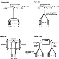
- Figures 1(a) to 1(f) show methods by which traffic can be added at an Optical Add Drop Node and comments regarding each method are included:
- the invention seeks to provide flexibility, gain to the source and suppression of the ASE noise.
- wavelength channels are added using a waveguide or fibre coupler, an amplifier and a switchable multiband band-stop filter, as shown in Figure 2 .
- Traffic is coupled into the single mode fibre. It is amplified along with all the other channels. Noise is added because of the amplified spontaneous emission in the amplifier.
- the switchable filter is set up so as to pass only the wavelength channels to be added.
- the switchable filter elements are set to have high loss in the wavelength bands of the e channels which are not being added.
- the filter then attenuates the broadband amplified spontaneous emission from the amplifier. This reduces the noise added to the ⁇ through' traffic channels.
- OADM nodes Numerical modelling has shown that attenuation of the ASE becomes important for bit rates of 21 ⁇ 2 and 10Gbit/s and above when traffic is required to pass through several OADM nodes in a ring.
- the OSNR Optical Signal to noise Ratio
- the use of the amplifier in the add channel path enables the number of add channels to be scaled to 32 and beyond.
- the amplifier allows lower power transmitter modules to be used.
- the switchable filter is required to attenuate the ASE by ⁇ 10dB to 15dB. Filter transmission loss for through channels of ⁇ 3dB would be viable.
- This approach allows low power tunable laser based transmitters to be used to add up to 32 channels and more.
- the channels can be added as the traffic builds so equipment can be added and financed as required on a 'pay as you grow' basis - or a "partial provisioning with growth as needed" basis..
- amplification and filtering may be used to keep the ASE within the limit to permit transmission through several nodes with acceptable signal to noise OSNR ratio.
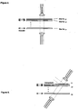
- the switchable multichannel filter may be implemented in one of a number of ways:
- This filter requires the reflection to be electrically retuned. To permit a channel to pass the reflector grating has to be tuned to sit in the wavelength band between two channels. This is restrictive on the packing of channels into a particular band. Also it needs programming, calibration and temperature control..
- a bleachable medium is Erbium doped P 2 O 3 glass.
- Erbium can have a high concentration in P 2 O 3 glass. 1 mm thick plate could have a few dB of loss.
- the radiative lifetime of erbium atoms is ⁇ 10 -2 seconds so once bleaching has occurred, it would not distort the digitally modulated signal which may have pulse lengths ⁇ sub nanoseconds.
- suitable dyes in polymer films are potential media for this as long as bleach lifetimes are significantly longer than the bit period of the traffic being passed through the filter.
- semiconductor bleachable media comprising Cadmium Telluride, or Cadmium Mercury Telluride, or Indium Gallium Arsenide Phosphide dad between Indium Phosphide layers for a double hetero-structure layer
- the absorber would be a semiconductor with bandgap less than the photon energy of the traffic and the intermediate (cladding) layers will have wider band gaps.
- a particularly favourable bleachable material for this purpose is a multilayer stack of InP/InGaAs/InP/InGaAs in which the Indium Gallium Arsenide layers are made 0.02 ⁇ m thick and the InP layers separating the InGaAs layers 0.01 to 0.03 ⁇ m thickness.
- a materials specification is given in the table below: Layer No.
- the attenuation of ASE is increased by having more GaInAs layers-10 is modelled to give 15dB attenuation for the reflection geometry described above.
- the GalnAs layer will bleach when power increases to ⁇ 100 w/cm 2 . If each channel is imaged to a spot of 8 ⁇ m diameter, then the bleach power will be ⁇ 50 ⁇ w. With 4 ⁇ diameter spot size the bleach power would be ⁇ 12 ⁇ w.
- ACG Arrayed Wave Guide
- a transmission configuration having a mux and demux stage could also be used effectively. Then no circulator would be required but lower net attenuation (from the single pass through the bleachable layer) would result and no reflector would be required.
- the laser wavelength is selected to conform to a particular tolerance within a standard grid - the ITU 100GHz or 50GHz Standard Grids for example
Landscapes
- Physics & Mathematics (AREA)
- Engineering & Computer Science (AREA)
- Computer Networks & Wireless Communication (AREA)
- Signal Processing (AREA)
- Optics & Photonics (AREA)
- General Physics & Mathematics (AREA)
- Nanotechnology (AREA)
- Nonlinear Science (AREA)
- Chemical & Material Sciences (AREA)
- Crystallography & Structural Chemistry (AREA)
- Biophysics (AREA)
- Life Sciences & Earth Sciences (AREA)
- Optical Communication System (AREA)
- Radio Transmission System (AREA)
- Stereo-Broadcasting Methods (AREA)
- Radar Systems Or Details Thereof (AREA)
Claims (15)
- Telekommunikationssystem, das eine Einmoden-Glasfaser umfasst, die Wellenlängenmultiplex- bzw. WDM-Verkehr überträgt, und einen Transmissionsfaserkoppler aufweist, der so ausgelegt ist, dass er hinzuzufügende Signale aus Kanälen in die Einmoden-Glasfaser einkoppelt, ferner umfassend Koppelmittel zum Verbinden der Kanäle, welche die hinzuzufügenden Signale übertragen, mit dem Eingang eines optischen Verstärkers, wobei der Ausgang des Verstärkers durch ein umschaltbares Mehrband-Bandstoppfilter, das so ausgelegt ist, dass es mit geringem Verlust nur Signale mit der Wellenlänge eines Signals oder von Signalen durchlässt, die dem WDM-Verkehr hinzugefügt werden sollen, und alle Signale bei Wellenlängen dämpft, die nicht die Wellenlänge des Signals oder der Signale aufweisen, die dem WDM-Verkehr hinzugefügt werden sollen, mit dem Transmissionsfaserkoppler in Reihe geschaltet ist, wobei das Bandstoppfilter insbesondere so ausgelegt ist, dass es Signale dämpft, welche als Ergebnis von verstärkter spontaner Emission erzeugt werden.
- Telekommunikationssystem nach Anspruch 1, wobei das umschaltbare Mehrband-Bandstoppfilter eine Reihe von Bragg-Fasergitterfiltern umfasst.
- Telekommunikationssystem nach Anspruch 1, wobei das umschaltbare Mehrband-Bandstoppfilter einen Stapel von selektiven Schmalband-Passfiltern und Betätigungsmitteln umfasst, um jeweilige Filter zu verschieben, um ausgewählte Kanäle durchzulassen.
- Telekommunikationssystem nach Anspruch 1, wobei das umschaltbare Mehrband-Bandstoppfilter einen Stapel von Beugungsgittern umfasst, wobei jeweilige Beugungsgitter entfernt oder aktiviert oder deaktiviert werden können, um ausgewählte Kanäle durchzulassen.
- Telekommunikationssystem nach Anspruch 1, wobei das umschaltbare Mehrband-Bandstoppfilter einen Lichtwellenlängenkanal-Demultiplexer, der so ausgelegt ist, dass er Wellenlängenkomponenten des Signals, das durch die Einmodenfaser übertragen wird, räumlich trennt, und einen bleichbaren Reflektor umfasst, der so ausgelegt ist, dass er die getrennten Wellenlängenkomponenten des Signals abfängt und mit geringem Verlust nur Signale mit der Wellenlänge eines Signals oder von Signalen durchlässt, die dem WDM-Verkehr hinzugefügt werden sollen, und alle Signale bei Wellenlängen dämpft, die nicht die Wellenlänge des Signals oder der Signale aufweisen, die dem DM-Verkehr hinzugefügt werden sollen.
- Telekommunikationssystem nach Anspruch 5, ferner umfassend einen Multiplexer, der so ausgelegt ist, dass er den Verkehr wieder in die Einmoden-Glasfaser zusammenfügt.
- Telekommunikationssystem nach Anspruch 5 oder 6, wobei der bleichbare Reflektor erbiumdotiertes Glas umfasst.
- Telekommunikationssystem nach Anspruch 5, 6 oder 7, wobei der bleichbare Reflektor ein thermisch aktiviertes bleichbares Medium umfasst.
- Telekommunikationssystem nach Anspruch 8, wobei die thermische Aktivierung durch die optischen Signale bereitgestellt wird.
- Telekommunikationssystem nach Anspruch 9, wobei die thermische Aktivierung durch die Photonenenergie der optischen Signale bereitgestellt wird.
- Telekommunikationssystem nach Anspruch 5, wobei der bleichbare Reflektor ein bleichbares Halbleitermedium umfasst.
- Telekommunikationssystem nach Anspruch 8, wobei das bleichbare Halbleitermedium einen Cadmium-Tellurid- oder Cadmium-Quecksilber-Tellurid- oder Indium-Gallium-Arsenid-Phosphid- oder Indium-Gallium-Arsenid-Mantel zwischen Indium-Phosphid-Schichten für eine Doppel-Heterostrukturschicht umfasst.
- Telekommunikationssystem nach Anspruch 9 oder 10, wobei es sich bei dem bleichbaren Material um einen Stapel von GaInAs-Schichten zwischen InP- oder InGaAsP-Schichten mit breiterem Spalt handelt, so dass die Bleichungsschwelle die von jeder einzelnen Schicht ist und die Dämpfung die Summe der Transmission durch die mehrfachen Schichten ist.
- Telekommunikationssystem nach Anspruch 6, wobei der Multiplexer und der Demultiplexer eine Wellenleiteranordnung umfassen.
- Teekommunikationssystem nach einem der Ansprüche 5 bis 14, ferner umfassend einen optischen Zirkulator.
Applications Claiming Priority (3)
| Application Number | Priority Date | Filing Date | Title |
|---|---|---|---|
| GBGB0111822.3A GB0111822D0 (en) | 2001-05-15 | 2001-05-15 | Signal addition to a wave division multiplex system |
| GB0111822 | 2001-05-15 | ||
| PCT/GB2002/000584 WO2002093806A1 (en) | 2001-05-15 | 2002-02-11 | Signal addition to a wave division multiplex system |
Publications (2)
| Publication Number | Publication Date |
|---|---|
| EP1391069A1 EP1391069A1 (de) | 2004-02-25 |
| EP1391069B1 true EP1391069B1 (de) | 2012-04-11 |
Family
ID=9914651
Family Applications (1)
| Application Number | Title | Priority Date | Filing Date |
|---|---|---|---|
| EP02711052A Expired - Lifetime EP1391069B1 (de) | 2001-05-15 | 2002-02-11 | Hinzufügen von signalen in einem mehrwellenlängen-multiplexsystem |
Country Status (9)
| Country | Link |
|---|---|
| US (1) | US7164816B2 (de) |
| EP (1) | EP1391069B1 (de) |
| JP (1) | JP4520700B2 (de) |
| CN (1) | CN1640043A (de) |
| AT (1) | ATE553557T1 (de) |
| CA (1) | CA2440442C (de) |
| DK (1) | DK1391069T3 (de) |
| GB (1) | GB0111822D0 (de) |
| WO (1) | WO2002093806A1 (de) |
Families Citing this family (5)
| Publication number | Priority date | Publication date | Assignee | Title |
|---|---|---|---|---|
| FR2863727B1 (fr) * | 2003-12-12 | 2006-03-03 | Thales Sa | Systeme optronique actif laser a detective amelioree |
| TWI563304B (en) * | 2012-05-22 | 2016-12-21 | Hon Hai Prec Ind Co Ltd | Laser signal transmitting device |
| US10069562B2 (en) * | 2016-10-11 | 2018-09-04 | X Development Llc | Optical circulator for free space optical communication |
| KR20200059356A (ko) * | 2018-11-20 | 2020-05-29 | 주식회사 오이솔루션 | 멀티채널 양방향 광통신 모듈 |
| CN113376748B (zh) * | 2021-06-17 | 2022-08-02 | 中国科学院半导体研究所 | 集成硅基布拉格反射器的合分波器件及制备方法 |
Family Cites Families (14)
| Publication number | Priority date | Publication date | Assignee | Title |
|---|---|---|---|---|
| JP2873856B2 (ja) * | 1990-04-03 | 1999-03-24 | キヤノン株式会社 | 光増幅器 |
| EP0478060B1 (de) | 1990-09-24 | 1995-12-06 | Philips Electronics Uk Limited | Optisch schaltbare Vorrichtung |
| JPH08237203A (ja) * | 1995-02-23 | 1996-09-13 | Fujitsu Ltd | 光フィルタアレイ、光送信機及び光送信システム |
| JP3039347B2 (ja) * | 1995-12-27 | 2000-05-08 | 日立電線株式会社 | スイッチング機能を備えた光部品及びそれに使用する導波路型フィルタ |
| JP4031853B2 (ja) | 1997-10-20 | 2008-01-09 | 富士通株式会社 | 双方向光通信用光伝送装置 |
| JP3259765B2 (ja) * | 1997-12-11 | 2002-02-25 | 住友電気工業株式会社 | 光入出力モジュール及び光反射器 |
| US6122299A (en) * | 1997-12-31 | 2000-09-19 | Sdl, Inc. | Angled distributed reflector optical device with enhanced light confinement |
| JPH11266234A (ja) | 1998-03-16 | 1999-09-28 | Alps Electric Co Ltd | 光通信装置 |
| JP3639109B2 (ja) | 1998-04-02 | 2005-04-20 | 富士通株式会社 | 光伝送装置、光伝送システム及び光端局 |
| US6091869A (en) * | 1998-04-30 | 2000-07-18 | Telefonaktiebolaget Lm Ericsson | Low loss, optical add/drop WDM node |
| EP0967752A2 (de) | 1998-06-24 | 1999-12-29 | Sumitomo Electric Industries, Ltd. | WDM Nachrichtenübertragungssystem |
| JP3401189B2 (ja) * | 1998-07-03 | 2003-04-28 | 日本電信電話株式会社 | 光アド・ドロップ装置 |
| AU760925B2 (en) | 1999-02-18 | 2003-05-22 | Xieon Networks S.A.R.L. | Add-drop-multiplexer and optical wavelength division multiplex transmission system |
| US6947670B1 (en) | 1999-06-30 | 2005-09-20 | Lucent Technologies Inc. | Optical add/drop arrangement for ring networks employing wavelength division multiplexing |
-
2001
- 2001-05-15 GB GBGB0111822.3A patent/GB0111822D0/en not_active Ceased
-
2002
- 2002-02-11 JP JP2002590558A patent/JP4520700B2/ja not_active Expired - Fee Related
- 2002-02-11 DK DK02711052.7T patent/DK1391069T3/da active
- 2002-02-11 WO PCT/GB2002/000584 patent/WO2002093806A1/en not_active Ceased
- 2002-02-11 CA CA2440442A patent/CA2440442C/en not_active Expired - Lifetime
- 2002-02-11 CN CNA028099605A patent/CN1640043A/zh active Pending
- 2002-02-11 US US10/472,665 patent/US7164816B2/en not_active Expired - Lifetime
- 2002-02-11 EP EP02711052A patent/EP1391069B1/de not_active Expired - Lifetime
- 2002-02-11 AT AT02711052T patent/ATE553557T1/de active
Also Published As
| Publication number | Publication date |
|---|---|
| GB0111822D0 (en) | 2001-07-04 |
| JP4520700B2 (ja) | 2010-08-11 |
| CA2440442C (en) | 2012-05-01 |
| WO2002093806A1 (en) | 2002-11-21 |
| CA2440442A1 (en) | 2002-11-21 |
| EP1391069A1 (de) | 2004-02-25 |
| DK1391069T3 (da) | 2012-05-29 |
| US7164816B2 (en) | 2007-01-16 |
| CN1640043A (zh) | 2005-07-13 |
| JP2004531960A (ja) | 2004-10-14 |
| ATE553557T1 (de) | 2012-04-15 |
| US20040151420A1 (en) | 2004-08-05 |
Similar Documents
| Publication | Publication Date | Title |
|---|---|---|
| Baxter et al. | Highly programmable wavelength selective switch based on liquid crystal on silicon switching elements | |
| EP1013022B1 (de) | Vorrichtung und verfahren zur optischen übertragungstechnik | |
| US6185023B1 (en) | Optical add-drop multiplexers compatible with very dense WDM optical communication systems | |
| US5446809A (en) | All fiber wavelength selective optical switch | |
| US6771905B1 (en) | Optical transmission systems including optical switching devices, control apparatuses, and methods | |
| US6959153B2 (en) | Dynamically reconfigurable add/drop multiplexer with low coherent cross-talk for optical communication networks | |
| US6904240B1 (en) | Optical multiplexing apparatus and optical multiplexing method | |
| US6845185B2 (en) | High-speed wavelength channel selector and high-speed photonic integrated circuit-type space and wavelength multiplexed channel selector employing the same | |
| US20060023996A1 (en) | Optical add/drop multiplexer | |
| Tran et al. | Reconfigurable multichannel optical add-drop multiplexers incorporating eight-port optical circulators and fiber Bragg gratings | |
| US20070258714A1 (en) | Wavelength division multiplexed optical communication system with rapidly-tunable optical filters | |
| US6516112B1 (en) | Optical wavelength filter and demultiplexer | |
| US6744986B1 (en) | Tunable wavelength add/drop multiplexer based on integrated optic devices | |
| EP1391069B1 (de) | Hinzufügen von signalen in einem mehrwellenlängen-multiplexsystem | |
| JP7797168B2 (ja) | 光信号処理装置 | |
| Nyman et al. | Technology trends in dense WDM demultiplexers | |
| JP3558199B2 (ja) | 光処理回路 | |
| US7113662B2 (en) | Optical filtering by using an add-drop node | |
| Zali et al. | Polarization insensitive photonic integrated 1x4 WDM wavelength selective switch for optical networks | |
| Feng et al. | Metro add-drop network applications of cascaded dispersion-compensated interleaver pairs using a recirculating loop | |
| Urquhart | Component technologies for future optical networks | |
| Hamel et al. | Optical filters in WDM ring network architectures | |
| Tian et al. | Novel fully dynamic and reconfigurable optical add/drop multiplexer based on AOTF with low crosstalk | |
| Chen et al. | Dynamically selective multiwavelength cross-connect based on fibre Bragg gratings and mechanical optical switches | |
| Stabile et al. | Sixteen-channel monolithically integrated InP wavelength selector based on a chain of passband-flattened cyclic AWG and optical switches |
Legal Events
| Date | Code | Title | Description |
|---|---|---|---|
| PUAI | Public reference made under article 153(3) epc to a published international application that has entered the european phase |
Free format text: ORIGINAL CODE: 0009012 |
|
| 17P | Request for examination filed |
Effective date: 20031212 |
|
| AK | Designated contracting states |
Kind code of ref document: A1 Designated state(s): AT BE CH CY DE DK ES FI FR GB GR IE IT LI LU MC NL PT SE TR |
|
| AX | Request for extension of the european patent |
Extension state: AL LT LV MK RO SI |
|
| RAP1 | Party data changed (applicant data changed or rights of an application transferred) |
Owner name: M(DGP1) LTD |
|
| RAP1 | Party data changed (applicant data changed or rights of an application transferred) |
Owner name: ERICSSON AB |
|
| RAP1 | Party data changed (applicant data changed or rights of an application transferred) |
Owner name: ERICSSON AB |
|
| 17Q | First examination report despatched |
Effective date: 20090903 |
|
| RAP1 | Party data changed (applicant data changed or rights of an application transferred) |
Owner name: ERICSSON AB |
|
| GRAP | Despatch of communication of intention to grant a patent |
Free format text: ORIGINAL CODE: EPIDOSNIGR1 |
|
| GRAS | Grant fee paid |
Free format text: ORIGINAL CODE: EPIDOSNIGR3 |
|
| GRAA | (expected) grant |
Free format text: ORIGINAL CODE: 0009210 |
|
| AK | Designated contracting states |
Kind code of ref document: B1 Designated state(s): AT BE CH CY DE DK ES FI FR GB GR IE IT LI LU MC NL PT SE TR |
|
| REG | Reference to a national code |
Ref country code: GB Ref legal event code: FG4D |
|
| REG | Reference to a national code |
Ref country code: CH Ref legal event code: EP |
|
| REG | Reference to a national code |
Ref country code: AT Ref legal event code: REF Ref document number: 553557 Country of ref document: AT Kind code of ref document: T Effective date: 20120415 |
|
| REG | Reference to a national code |
Ref country code: IE Ref legal event code: FG4D |
|
| REG | Reference to a national code |
Ref country code: DK Ref legal event code: T3 |
|
| REG | Reference to a national code |
Ref country code: DE Ref legal event code: R096 Ref document number: 60242620 Country of ref document: DE Effective date: 20120531 |
|
| REG | Reference to a national code |
Ref country code: NL Ref legal event code: T3 |
|
| REG | Reference to a national code |
Ref country code: AT Ref legal event code: MK05 Ref document number: 553557 Country of ref document: AT Kind code of ref document: T Effective date: 20120411 |
|
| PG25 | Lapsed in a contracting state [announced via postgrant information from national office to epo] |
Ref country code: FI Free format text: LAPSE BECAUSE OF FAILURE TO SUBMIT A TRANSLATION OF THE DESCRIPTION OR TO PAY THE FEE WITHIN THE PRESCRIBED TIME-LIMIT Effective date: 20120411 Ref country code: CY Free format text: LAPSE BECAUSE OF FAILURE TO SUBMIT A TRANSLATION OF THE DESCRIPTION OR TO PAY THE FEE WITHIN THE PRESCRIBED TIME-LIMIT Effective date: 20120411 Ref country code: SE Free format text: LAPSE BECAUSE OF FAILURE TO SUBMIT A TRANSLATION OF THE DESCRIPTION OR TO PAY THE FEE WITHIN THE PRESCRIBED TIME-LIMIT Effective date: 20120411 |
|
| PG25 | Lapsed in a contracting state [announced via postgrant information from national office to epo] |
Ref country code: PT Free format text: LAPSE BECAUSE OF FAILURE TO SUBMIT A TRANSLATION OF THE DESCRIPTION OR TO PAY THE FEE WITHIN THE PRESCRIBED TIME-LIMIT Effective date: 20120813 Ref country code: GR Free format text: LAPSE BECAUSE OF FAILURE TO SUBMIT A TRANSLATION OF THE DESCRIPTION OR TO PAY THE FEE WITHIN THE PRESCRIBED TIME-LIMIT Effective date: 20120712 |
|
| PG25 | Lapsed in a contracting state [announced via postgrant information from national office to epo] |
Ref country code: AT Free format text: LAPSE BECAUSE OF FAILURE TO SUBMIT A TRANSLATION OF THE DESCRIPTION OR TO PAY THE FEE WITHIN THE PRESCRIBED TIME-LIMIT Effective date: 20120411 |
|
| PLBE | No opposition filed within time limit |
Free format text: ORIGINAL CODE: 0009261 |
|
| STAA | Information on the status of an ep patent application or granted ep patent |
Free format text: STATUS: NO OPPOSITION FILED WITHIN TIME LIMIT |
|
| PG25 | Lapsed in a contracting state [announced via postgrant information from national office to epo] |
Ref country code: IT Free format text: LAPSE BECAUSE OF FAILURE TO SUBMIT A TRANSLATION OF THE DESCRIPTION OR TO PAY THE FEE WITHIN THE PRESCRIBED TIME-LIMIT Effective date: 20120411 |
|
| 26N | No opposition filed |
Effective date: 20130114 |
|
| PG25 | Lapsed in a contracting state [announced via postgrant information from national office to epo] |
Ref country code: ES Free format text: LAPSE BECAUSE OF FAILURE TO SUBMIT A TRANSLATION OF THE DESCRIPTION OR TO PAY THE FEE WITHIN THE PRESCRIBED TIME-LIMIT Effective date: 20120722 |
|
| REG | Reference to a national code |
Ref country code: DE Ref legal event code: R097 Ref document number: 60242620 Country of ref document: DE Effective date: 20130114 |
|
| PG25 | Lapsed in a contracting state [announced via postgrant information from national office to epo] |
Ref country code: MC Free format text: LAPSE BECAUSE OF NON-PAYMENT OF DUE FEES Effective date: 20130228 |
|
| REG | Reference to a national code |
Ref country code: CH Ref legal event code: PL |
|
| PG25 | Lapsed in a contracting state [announced via postgrant information from national office to epo] |
Ref country code: LI Free format text: LAPSE BECAUSE OF NON-PAYMENT OF DUE FEES Effective date: 20130228 Ref country code: CH Free format text: LAPSE BECAUSE OF NON-PAYMENT OF DUE FEES Effective date: 20130228 |
|
| REG | Reference to a national code |
Ref country code: IE Ref legal event code: MM4A |
|
| PG25 | Lapsed in a contracting state [announced via postgrant information from national office to epo] |
Ref country code: IE Free format text: LAPSE BECAUSE OF NON-PAYMENT OF DUE FEES Effective date: 20130211 |
|
| PG25 | Lapsed in a contracting state [announced via postgrant information from national office to epo] |
Ref country code: TR Free format text: LAPSE BECAUSE OF FAILURE TO SUBMIT A TRANSLATION OF THE DESCRIPTION OR TO PAY THE FEE WITHIN THE PRESCRIBED TIME-LIMIT Effective date: 20120411 |
|
| PG25 | Lapsed in a contracting state [announced via postgrant information from national office to epo] |
Ref country code: LU Free format text: LAPSE BECAUSE OF NON-PAYMENT OF DUE FEES Effective date: 20130211 |
|
| REG | Reference to a national code |
Ref country code: FR Ref legal event code: PLFP Year of fee payment: 15 |
|
| PGFP | Annual fee paid to national office [announced via postgrant information from national office to epo] |
Ref country code: NL Payment date: 20160225 Year of fee payment: 15 Ref country code: DK Payment date: 20160224 Year of fee payment: 15 Ref country code: DE Payment date: 20160226 Year of fee payment: 15 |
|
| PGFP | Annual fee paid to national office [announced via postgrant information from national office to epo] |
Ref country code: BE Payment date: 20160226 Year of fee payment: 15 Ref country code: GB Payment date: 20160226 Year of fee payment: 15 Ref country code: FR Payment date: 20160217 Year of fee payment: 15 |
|
| PG25 | Lapsed in a contracting state [announced via postgrant information from national office to epo] |
Ref country code: BE Free format text: LAPSE BECAUSE OF NON-PAYMENT OF DUE FEES Effective date: 20170228 |
|
| REG | Reference to a national code |
Ref country code: DE Ref legal event code: R119 Ref document number: 60242620 Country of ref document: DE |
|
| REG | Reference to a national code |
Ref country code: DK Ref legal event code: EBP Effective date: 20170228 |
|
| REG | Reference to a national code |
Ref country code: NL Ref legal event code: MM Effective date: 20170301 |
|
| GBPC | Gb: european patent ceased through non-payment of renewal fee |
Effective date: 20170211 |
|
| PG25 | Lapsed in a contracting state [announced via postgrant information from national office to epo] |
Ref country code: NL Free format text: LAPSE BECAUSE OF NON-PAYMENT OF DUE FEES Effective date: 20170301 |
|
| REG | Reference to a national code |
Ref country code: FR Ref legal event code: ST Effective date: 20171031 |
|
| PG25 | Lapsed in a contracting state [announced via postgrant information from national office to epo] |
Ref country code: FR Free format text: LAPSE BECAUSE OF NON-PAYMENT OF DUE FEES Effective date: 20170228 Ref country code: DK Free format text: LAPSE BECAUSE OF NON-PAYMENT OF DUE FEES Effective date: 20170228 Ref country code: DE Free format text: LAPSE BECAUSE OF NON-PAYMENT OF DUE FEES Effective date: 20170901 |
|
| REG | Reference to a national code |
Ref country code: BE Ref legal event code: MM Effective date: 20170228 |
|
| PG25 | Lapsed in a contracting state [announced via postgrant information from national office to epo] |
Ref country code: GB Free format text: LAPSE BECAUSE OF NON-PAYMENT OF DUE FEES Effective date: 20170211 |