EP1390809B1 - Compositions pour microcellules d'un affichage electrophoretique - Google Patents
Compositions pour microcellules d'un affichage electrophoretique Download PDFInfo
- Publication number
- EP1390809B1 EP1390809B1 EP02731451A EP02731451A EP1390809B1 EP 1390809 B1 EP1390809 B1 EP 1390809B1 EP 02731451 A EP02731451 A EP 02731451A EP 02731451 A EP02731451 A EP 02731451A EP 1390809 B1 EP1390809 B1 EP 1390809B1
- Authority
- EP
- European Patent Office
- Prior art keywords
- electrophoretic display
- rubber material
- rubber
- microcup
- radiation curable
- Prior art date
- Legal status (The legal status is an assumption and is not a legal conclusion. Google has not performed a legal analysis and makes no representation as to the accuracy of the status listed.)
- Expired - Lifetime
Links
Images

Classifications
-
- G—PHYSICS
- G02—OPTICS
- G02F—OPTICAL DEVICES OR ARRANGEMENTS FOR THE CONTROL OF LIGHT BY MODIFICATION OF THE OPTICAL PROPERTIES OF THE MEDIA OF THE ELEMENTS INVOLVED THEREIN; NON-LINEAR OPTICS; FREQUENCY-CHANGING OF LIGHT; OPTICAL LOGIC ELEMENTS; OPTICAL ANALOGUE/DIGITAL CONVERTERS
- G02F1/00—Devices or arrangements for the control of the intensity, colour, phase, polarisation or direction of light arriving from an independent light source, e.g. switching, gating or modulating; Non-linear optics
- G02F1/01—Devices or arrangements for the control of the intensity, colour, phase, polarisation or direction of light arriving from an independent light source, e.g. switching, gating or modulating; Non-linear optics for the control of the intensity, phase, polarisation or colour
- G02F1/165—Devices or arrangements for the control of the intensity, colour, phase, polarisation or direction of light arriving from an independent light source, e.g. switching, gating or modulating; Non-linear optics for the control of the intensity, phase, polarisation or colour based on translational movement of particles in a fluid under the influence of an applied field
- G02F1/166—Devices or arrangements for the control of the intensity, colour, phase, polarisation or direction of light arriving from an independent light source, e.g. switching, gating or modulating; Non-linear optics for the control of the intensity, phase, polarisation or colour based on translational movement of particles in a fluid under the influence of an applied field characterised by the electro-optical or magneto-optical effect
- G02F1/167—Devices or arrangements for the control of the intensity, colour, phase, polarisation or direction of light arriving from an independent light source, e.g. switching, gating or modulating; Non-linear optics for the control of the intensity, phase, polarisation or colour based on translational movement of particles in a fluid under the influence of an applied field characterised by the electro-optical or magneto-optical effect by electrophoresis
-
- Y—GENERAL TAGGING OF NEW TECHNOLOGICAL DEVELOPMENTS; GENERAL TAGGING OF CROSS-SECTIONAL TECHNOLOGIES SPANNING OVER SEVERAL SECTIONS OF THE IPC; TECHNICAL SUBJECTS COVERED BY FORMER USPC CROSS-REFERENCE ART COLLECTIONS [XRACs] AND DIGESTS
- Y10—TECHNICAL SUBJECTS COVERED BY FORMER USPC
- Y10S—TECHNICAL SUBJECTS COVERED BY FORMER USPC CROSS-REFERENCE ART COLLECTIONS [XRACs] AND DIGESTS
- Y10S428/00—Stock material or miscellaneous articles
- Y10S428/913—Material designed to be responsive to temperature, light, moisture
-
- Y—GENERAL TAGGING OF NEW TECHNOLOGICAL DEVELOPMENTS; GENERAL TAGGING OF CROSS-SECTIONAL TECHNOLOGIES SPANNING OVER SEVERAL SECTIONS OF THE IPC; TECHNICAL SUBJECTS COVERED BY FORMER USPC CROSS-REFERENCE ART COLLECTIONS [XRACs] AND DIGESTS
- Y10—TECHNICAL SUBJECTS COVERED BY FORMER USPC
- Y10T—TECHNICAL SUBJECTS COVERED BY FORMER US CLASSIFICATION
- Y10T428/00—Stock material or miscellaneous articles
- Y10T428/23—Sheet including cover or casing
- Y10T428/234—Sheet including cover or casing including elements cooperating to form cells
- Y10T428/236—Honeycomb type cells extend perpendicularly to nonthickness layer
-
- Y—GENERAL TAGGING OF NEW TECHNOLOGICAL DEVELOPMENTS; GENERAL TAGGING OF CROSS-SECTIONAL TECHNOLOGIES SPANNING OVER SEVERAL SECTIONS OF THE IPC; TECHNICAL SUBJECTS COVERED BY FORMER USPC CROSS-REFERENCE ART COLLECTIONS [XRACs] AND DIGESTS
- Y10—TECHNICAL SUBJECTS COVERED BY FORMER USPC
- Y10T—TECHNICAL SUBJECTS COVERED BY FORMER US CLASSIFICATION
- Y10T428/00—Stock material or miscellaneous articles
- Y10T428/24—Structurally defined web or sheet [e.g., overall dimension, etc.]
- Y10T428/24479—Structurally defined web or sheet [e.g., overall dimension, etc.] including variation in thickness
- Y10T428/24562—Interlaminar spaces
-
- Y—GENERAL TAGGING OF NEW TECHNOLOGICAL DEVELOPMENTS; GENERAL TAGGING OF CROSS-SECTIONAL TECHNOLOGIES SPANNING OVER SEVERAL SECTIONS OF THE IPC; TECHNICAL SUBJECTS COVERED BY FORMER USPC CROSS-REFERENCE ART COLLECTIONS [XRACs] AND DIGESTS
- Y10—TECHNICAL SUBJECTS COVERED BY FORMER USPC
- Y10T—TECHNICAL SUBJECTS COVERED BY FORMER US CLASSIFICATION
- Y10T428/00—Stock material or miscellaneous articles
- Y10T428/24—Structurally defined web or sheet [e.g., overall dimension, etc.]
- Y10T428/24479—Structurally defined web or sheet [e.g., overall dimension, etc.] including variation in thickness
- Y10T428/24612—Composite web or sheet
Definitions
- the electrophoretic display is a non-emissive device based on the electrophoresis phenomenon influencing charged pigment particles suspended in a solvent This general type of display was first proposed in 1969.
- An electrophoretic display typically comprises a pair of opposed, spaced-apart plate-like electrodes, with spacers predetermining a certain distance between the electrodes.
- One of the electrodes is typically transparent.
- a dispersion composed of a colored solvent and suspended charged pigment particles is enclosed between the two plates.
- the pigment particles migrate to one side by attraction to the plate of polarity opposite that of the pigment particles.
- the color showing at the transparent plate may be determined by selectively charging the plates to be either the color of the solvent or the color of the pigment particles. Reversal of plate polarity will cause the particles to migrate back to the opposite plate, thereby reversing the color.
- Intermediate color density (or shades of grey) due to intermediate pigment density at the transparent plate may be obtained by controlling the plate charge through a range of voltages.
- the microencapsulated electrophoretic display has a substantially two dimensional arrangement of microcapsules each having therein an electrophoretic composition of a dielectric fluid and a dispersion of charged pigment particles that visually contrast with the dielectric solvent.
- the improved electrophoretic display comprises cells formed from microcups of well-defined shape, size, and aspect ratio and filled with charged pigment particles dispersed in a dielectric solvent.
- Multifunctional UV curable compositions have been employed to fabricate the microcup array for the improved electrophoretic display.
- the microcup structure formed tends to be quite brittle.
- the internal stress in the cups due to the high degree of crosslinking and shrinkage often results in undesirable cracking and delamination of the microcups from the conductor substrate during demolding.
- the microcup array prepared from the multifunctional UV curable compositions also showed a poor flexure resistance.
- Suitable rubber materials for this purpose include SBR (styrene-butadiene rubber), PBR (polybutadiene rubber), NBR (acrylonitrile-butadiene rubber), SBS (styrene-butadiene-styrene block copolymer), SIS (styrene-isoprene-styrene block copolymer), and their derivatives.
- SBR styrene-butadiene rubber
- PBR polybutadiene rubber
- NBR acrylonitrile-butadiene rubber
- SBS styrene-butadiene-styrene block copolymer
- SIS styrene-isoprene-styrene block copolymer
- polybutadiene dimethacrylate CN301 and CN302 from Sartomer
- Ricacryl 3100 from Ricon Resins Inc.
- graft (meth)acrylated hydrocarbon polymer Rostomer
- Ricacryl 3500 and Ricacryl 3801 from Ricon Resins, Inc.
- methacrylate terminated butadiene-acrylonitrile copolymers Hycar VTBNX 1300 ⁇ 33, 1300 ⁇ 43 from BFGoodrich
- microcup Unless defined otherwise in this specification, all technical terms are used herein according to their conventional definitions as they are commonly used and understood by those of ordinary skill in the art.
- the terms "microcup”, “cell”, “well-defined”, “aspect ratio” and “imagewise exposure” in the context of the present application are as defined in the copending applications identified above, so are the dimensions of the microcups.
- the microcups may be prepared by microembossing or by photolithography.
- the male mold may be prepared by any appropriate method, such as a diamond turn process or a photoresist process followed by either etching or electroplating.
- a master template for the male mold may be manufactured by any appropriate method, such as electroplating. With electroplating, a glass base is sputtered with a thin layer (typically 3000 ⁇ ) of a seed metal such as chrome inconel. It is then coated with a layer of photoresist and exposed to UV. A mask is placed between the UV and the layer of photoresist. The exposed areas of the photoresist become hardened. The unexposed areas are then removed by washing them with an appropriate solvent The remaining hardened photoresist is dried and sputtered again with a thin layer of seed metal.
- a master is then ready for electroforming.
- a typical material used for electroforming is nickel cobalt.
- the master can be made of nickel by electroforming or electroless nickel deposition as described in "Continuous manufacturing of thin cover sheet optical media", SPIE Proc. Vol. 1663, pp.324 (1992).
- the floor of the mold is typically between about 50 to 400 microns.
- the master can also be made using other microengineering techniques including e-beam writing, dry etching, chemical etching, laser writing or laser interference as described in "Replication techniques for micro-optics", SPIE Proc. Vol.3099, pp76-82 (1997).
- the mold can be made by photomachining, using plastics, ceramics or metals.
- the male mold thus prepared typically has protrusions between about 1 to 500 microns, preferably between about 2 to 100 microns, and most preferably about 4 to 50 microns.
- the male mold may be in the form of a belt, a roller, or a sheet.
- the belt type of mold is preferred.
- Micro-cups may be formed either in a batchwise process or in a continuous roll-to-roll process as disclosed in the co-pending application, US Serial Number 09/784,972, filed on February 25, 2001.
- the latter offers a continuous, low cost, high throughput manufacturing technology for production of compartments for use in electrophoretic or liquid crystal displays.
- the male mold Prior to applying a UV curable resin composition, the male mold may be treated with a mold release, if desired, to aid in the demolding process.
- the UV curable resin may be degassed prior to dispensing and may optionally contain a solvent. The solvent, if present, readily evaporates.
- the UV curable resin is dispensed by any appropriate means, such as coating, dipping, pouring and the like, over the male mold.
- the dispenser may be moving or stationary.
- a conductor film is overlaid on the UV curable resin. Examples of suitable conductor films include transparent conductor ITO on plastic substrates such as polyethylene terephthalate, polyethylene naphthate, polyaramid, polyimide, polycycloolefin, polysulfone, epoxy and their composites.
- Pressure may be applied, if necessary, to ensure proper bonding between the resin and the plastic and to control the thickness of the floor of the micro-cups.
- the pressure may be applied using a laminating roller, vacuum molding, press device or any other like means.
- the male mold is metallic and opaque, the plastic substrate is typically transparent to the actinic radiation used to cure the resin. Conversely, the male mold can be transparent and the plastic substrate can be opaque to the actinic radiation. To obtain good transfer of the molded features onto the transfer sheet, the conductor film needs to have good adhesion to the UV curable resin, which should have a good release property from the mold surface.
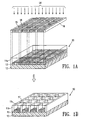
- the microcup array 10 may be prepared by exposure of a radiation curable material 11a coated by known methods onto a conductor electrode film 12 to UV light (or alternatively other forms of radiation, electron beams and the like) through a mask 16 to form walls 11b corresponding to the image projected through the mask 16.
- the base conductor film 12 is preferably mounted on a supportive substrate base web 13, which may comprise a plastic material.
- the dark squares 14 represent the opaque area and the space between the dark squares represents the opening (transparent) area 15 of the mask 16.
- the UV radiates through the opening area 15 onto the radiation curable material 11a.
- the exposure is preferably directly onto the radiation curable material 11a, i.e., the UV does not pass through the substrate 13 or base conductor 12 (top exposure). For this reason, neither the substrate 13 nor the conductor 12 needs to be transparent to the UV or other radiation wavelengths employed.
- the exposed areas 11b become hardened and the unexposed areas 11c (protected by the opaque area 14 of the mask 16 are then removed by an appropriate solvent or developer to form the microcups 17.
- the solvent or developer is selected from those commonly used for dissolving or reducing the viscosity of radiation curable materials such as methylethylketone, toluene, acetone, isopropanol or the like.
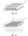
- the conductor film 22 used is pre-patterned to comprise cell base electrode portions 24 corresponding to the floor portions of the microcups 27.
- the base portions 24 are opaque to the UV wavelength (or other radiation) employed.
- the spaces 25 between conductor base portions 22 are substantially transparent or transmissive to the UV light.
- the conductor pattern serves as a photomask.
- the radiation curable material 21a is coated upon the substrate 23 and conductor 22 as described in Fig. 2A.
- the material 21a is exposed by UV light projected "upwards" (through substrate 23) and cured where not shielded by the conductor 22, i.e., in those areas corresponding to the space 25.
- the uncured material 21c is removed from the unexposed areas as described above, leaving the cured material 21b to form the walls of the microcups 27.
- Fig. 3A illustrates a combination method which uses both the top and bottom exposure principals to produce the microcup array 30 of the invention.
- the base conductor film 32 is also opaque and line-patterned.
- the radiation curable material 31a which is coated on the base conductor 32 and substrate 33, is exposed from the bottom through the conductor line pattern 32 which serves as the first photomask.
- a second exposure is performed from the "top" side through the second photomask 36 having a line pattern perpendicular to the conductor lines 32.
- the spaces 35 between the lines 34 are substantially transparent or transmissive to the UV light.
- the wall material 31b is cured from the bottom up in one lateral orientation, and cured from the top down in the perpendicular direction, joining to form an integral microcup 37.
- the unexposed area is then removed by a solvent or developer as described above to reveal the microcups 37.
- the radiation curable material used in the processes described above is a thermoplastic or thermoset precursor, such as multifunctional acrylate or methacrylate, vinylether, epoxide and their oligomers, polymers and the like. Multifunctional acrylates and their oligomers are the most preferred. A combination of multifunctional epoxide and multifunctional acrylate is also very useful to achieve desirable physico-mechanical properties.
- Suitable rubber materials have a Tg (glass transition temperature) lower than 0°C.
- Unsaturated rubber materials are preferred and rubber materials having uncapped or side chain unsaturated groups such as vinyl, acrylate, methacrylate, allyl groups are particularly preferred. More specifically, suitable rubber materials include SBR (styrene-butadiene rubber), PBR (polybutadiene rubber), NBR (acrylonitrile-butadiene rubber), SBS (styrene-butadiene-styrene block copolymer), SIS (styrene-isoprene-styrene block copolymer), and their derivatives.
- SBR styrene-butadiene rubber
- PBR polybutadiene rubber
- NBR acrylonitrile-butadiene rubber
- SBS styrene-butadiene-styrene block copolymer
- SIS styrene-isoprene-st
- polybutadiene dimethacrylate CN301 and CN302 from Sartomer
- Ricacryl 3100 from Ricon Resins Inc.
- graft (meth)acrylated hydrocarbon polymer Rostomer
- Ricacryl 3500 and Ricacryl 3801 from Ricon Resins, Inc.
- methacrylate terminated butadiene-acrylonitrile copolymers Hycar VTBNX 1300 ⁇ 33, 1300 ⁇ 43 from BFGoodrich
- the percentage of rubber component in the UV curable formulation can be in the range from 1 wt-% to 30 wt-%, preferably from 5 wt-% to 20 wt-%, even more preferably from 8-15 wt-%.
- the rubber components can be soluble or dispersible in the formulation. Ideally, the rubber component is soluble in the formulation before UV curing and phase separates into microdomains after UV curing.
- Example 1 Microcup composition without rubber
- Ebercryl® 600 35 parts by weight of Ebercryl® 600 (UCB), 40 parts of SR-399 (Sartomer®), 10 parts of Ebecryl 4827 (UCB), 7 parts of Ebecryl 1360 (UCB), 8 parts of HDDA (UCB), and 0.05 parts of Irgacure® 369 (Ciba Specialty Chemicals), 0.01 parts of isopropyl thioxanthone (Aldrich) were mixed homogeneously and used to prepare the microcup arrary by either the microembossing or photolithographic process.
- Example 2-7 The same procedure as Example 1 was repeated except that 6,7,8,10,11 or 14 phr (parts per hundred resin) of Hycar® VTBNX 1300 ⁇ 33 were added to the compositions of Examples 2-7, respectively.
- microcup compositions of Examples 1-7 were coated onto 2 mil PET film with a targeted dry thickness of about 30 ⁇ m, covered by untreated PET, and then cured for 20 seconds under UV light at an intensity of ⁇ 5 mW/cm 2 .
- the coated samples were then 90 degree hand bended to determine the flexure resistance, after the untreated PET was removed. It was found that the flexure resistance of formulations containing more than 8 phr of Hycar VTBNX 1300 ⁇ 33 (Examples 4,5,6,7) was improved significantly (Table 1).
- microcup compositions of the Example 1-7 were coated onto 2 mil PET film with a targeted thickness of about 50 ⁇ m, microembossed with a Ni-Co male mold of 60x60x35 ⁇ m with partition lines of 10 ⁇ m width, UV cured for 20 seconds, and removed from the mold with a 2" peeling bar at a speed of about 4-5 ft/min.
- the formulations containing more than 6 phr of rubber (Examples 2-7) showed significantly improved demoldability (Table 1). Little defect or contamination on the mold was observed for formulations containing 10-15 phr of rubber (Examples 5,6,7) after at least 100 molding-demolding cycles
- Example 1-7 The microcup compositions of Example 1-7 were coated onto 2 mil PET film with a targeted dry thickness of about 30 ⁇ m, covered by untreated PET, and then cured for 20 seconds under UV light at an intensity of ⁇ 5 mW/cm 2 .
- the untreated PET cover sheet was removed.
- a 15 wt% solution of the sealing material (Kraton® FG-1901X from Shell) in 20/80 (v/v) toluene/hexane was then coated onto the cured microcup layer and dried in 60 °C oven for 10 minutes. The thickness of the dried sealing layer was controlled to be about 5 ⁇ m.
- a 3M 3710 Scotch® tape was laminated at room temperature onto the sealing layer by a Eagle® 35 laminator from GBC at the heavy gauge setting.
- the T-peel adhesion force was then measured by Instron® at 500 mm/min.
- the adhesion forces listed in Table 1 were the average of at least 5 measurements. It was found that adhesion between the sealing layer and the cured microcup layer was significantly improved by incorporating rubber into the microcup.
- Example 8 Microcup composition without rubber
- Example 9 Microcup composition with rubber
- Example 8 The same procedure as in Example 8 was repeated except that 5.47 parts of poly(butadiene-co-acrylonitrile) diacrylate (Monomer-Polymer & Dajac Labs, Inc.) was added to the composition. No observable defect on the microcup array or contamination on the Ni-Co male mold was found after about 10 molding-demolding cycles.
- poly(butadiene-co-acrylonitrile) diacrylate Monomer-Polymer & Dajac Labs, Inc.
- Example 10 The same as in Example 10, except the Ti Pure R706 and Fluorolink were replaced by polymer coated TiO 2 particles PC-9003 from Elimentis (Hihstown, NJ) and Krytox® (Du Pont) respectively.
- the electrophoretic fluid prepared in Examples 10 was diluted with a volatile perfluoro cosolvent (FC-33 from 3M) and coated onto a microcup array containing 11 phr of Hycar® VTBNX 1300 ⁇ 33 (Example 6) on a ITO/PET conductor film.
- the volatile cosolvent was allowed to evaporate to expose a partially filled microcup array.
- a 7.5% solution of polyisoprene in heptane was then overcoated onto the partially filled cups by a Universal Blade Applicator with an opening of 6 mil.
- the overcoated microcups were then dried at room temperature.
- a seamless sealing layer of about 5-6 microns thickness with acceptable adhesion was formed on the microcup array.
- the electrophoretic fluid prepared in Example 11 was diluted with a volatile perfluoro cosolvent (FC-33 from 3M) and coated onto a microcup array containing 12 phr of Hycar® VTBNX 1300 ⁇ 33 on a ITO/PET conductor film.
- the volatile cosolvent was allowed to evaporate to expose a partially filled microcup array.
- a 7.5% solution of polyisoprene in heptane was then overcoated onto the partially filled cups by a Universal Blade Applicator with an opening of 6 mil.
- the overcoated microcups were then dried at room temperature.
- a seamless sealing layer of about 5-6 microns thickness with acceptable adhesion was form on the microcup array. No observable entrapped air bubbles in the sealed microcups were found under microscope.
- the sealed microcup array was then post treated by UV radiation or thermal baking to further improve the barrier properties.
- a second ITO/PET conductor precoated with an adhesive layer was laminated onto the sealed microcups.
- the electrophoretic cell showed satisfactory switching performance with good flexure resistance. No observable weight loss was found after aged in a 66 °C oven for 5 days.
- microcups may also be used for manufacturing microcup arrays for liquid crystal displays.
- microcup selective filling, sealing and ITO laminating methods of the invention may also be employed in the manufacture of liquid crystal displays.
Claims (15)
- Système d'affichage électrophorétique, qui comprend des cellules dont les parois sont constituées d'une composition comprenant une matière durcissable par les rayonnements et une matière caoutchouteuse.
- Système d'affichage électrophorétique selon la revendication 1, pour lequel la matière durcissable par les rayonnements est un précurseur d'une matière thermoplastique ou thermodurcissable.
- Système d'affichage électrophorétique selon la revendication 2, pour lequel ledit précurseur de matière thermoplastique ou thermodurcissable est un acrylate ou méthacrylate multifonctionnel, un éther vinylique, un époxyde ou un oligomère ou polymère de ces produits, ou un produit analogue.
- Système d'affichage électrophorétique selon la revendication 3, pour lequel ledit précurseur de matière thermoplastique ou thermodurcissable est un acrylate multifonctionnel ou un oligomère d'un tel acrylate.
- Système d'affichage électrophorétique selon la revendication 2, pour lequel ladite matière durcissable par les rayonnements est une combinaison d'un époxyde multifonctionnel et d'un acrylate multifonctionnel.
- Système d'affichage électrophorétique selon la revendication 1, pour lequel la matière caoutchouteuse est une matière ayant une température de transition vitreuse inférieure à environ 0 °C.
- Système d'affichage électrophorétique selon la revendication 6, pour lequel la matière caoutchouteuse est une matière insaturée.
- Système d'affichage électrophorétique selon la revendication 7, pour lequel la matière caoutchouteuse est une matière ayant des groupes insaturés non-coiffés ou en chaíne latérale, tels que des groupes vinyle, acrylate, méthacrylate ou allyle.
- Système d'affichage électrophorétique selon la revendication 1, pour lequel ladite matière caoutchouteuse est choisie parmi le caoutchouc styrène-butadiène (SBR), le caoutchouc polybutadiène (PBR), le caoutchouc acrylonitrile-butadiène (NBR), les copolymères séquencés styrène-butadiène-styrène (SBS), les copolymères séquencés styrène-isoprène-styrène (SIS), et leurs dérivés.
- Système d'affichage électrophorétique selon la revendication 9, pour lequel ladite matière caoutchouteuse est du diméthacrylate de polybutadiène, un polymère hydrocarboné acrylé ou méthacrylé par greffage, ou un copolymère de butadiène et d'acrylonitrile, à terminaison méthacrylate.
- Système d'affichage électrophorétique selon la revendication 1, pour lequel ladite composition comprend d'environ 1 à environ 30 % en poids de matière caoutchouteuse.
- Système d'affichage électrophorétique selon la revendication 11, pour lequel ladite composition comprend d'environ 5 à environ 20 % en poids de matière caoutchouteuse.
- Système d'affichage électrophorétique selon la revendication 12, pour lequel ladite composition comprend d'environ 8 à environ 15 % en poids de matière caoutchouteuse.
- Procédé de fabrication d'un système d'affichage électrophorétique, qui comprend la formation de microcoupelles par microestampage, procédé dans lequel on utilise une composition comprenant une matière durcissable par les rayonnements et une matière caoutchouteuse.
- Procédé de fabrication d'un système d'affichage électrophorétique, qui comprend la formation de microcoupelles par photolithographie, procédé dans lequel on utilise une composition comprenant une matière durcissable par les rayonnements et une matière caoutchouteuse.
Applications Claiming Priority (3)
| Application Number | Priority Date | Filing Date | Title |
|---|---|---|---|
| US09/840,756 US6753067B2 (en) | 2001-04-23 | 2001-04-23 | Microcup compositions having improved flexure resistance and release properties |
| US840756 | 2001-04-23 | ||
| PCT/US2002/012594 WO2002086613A2 (fr) | 2001-04-23 | 2002-04-22 | Compositions de micro-cellule possedant une resistance a la flexion et des proprietes de decollement ameliorees |
Publications (2)
| Publication Number | Publication Date |
|---|---|
| EP1390809A2 EP1390809A2 (fr) | 2004-02-25 |
| EP1390809B1 true EP1390809B1 (fr) | 2004-09-29 |
Family
ID=25283136
Family Applications (1)
| Application Number | Title | Priority Date | Filing Date |
|---|---|---|---|
| EP02731451A Expired - Lifetime EP1390809B1 (fr) | 2001-04-23 | 2002-04-22 | Compositions pour microcellules d'un affichage electrophoretique |
Country Status (9)
| Country | Link |
|---|---|
| US (4) | US6753067B2 (fr) |
| EP (1) | EP1390809B1 (fr) |
| JP (1) | JP4422965B2 (fr) |
| KR (1) | KR20030090768A (fr) |
| CN (1) | CN1172215C (fr) |
| AT (1) | ATE278205T1 (fr) |
| DE (1) | DE60201442T2 (fr) |
| TW (1) | TWI308249B (fr) |
| WO (1) | WO2002086613A2 (fr) |
Cited By (1)
| Publication number | Priority date | Publication date | Assignee | Title |
|---|---|---|---|---|
| US8361356B2 (en) | 2001-06-04 | 2013-01-29 | Sipix Imaging, Inc. | Composition and process for the sealing of microcups in roll-to-roll display manufacturing |
Families Citing this family (56)
| Publication number | Priority date | Publication date | Assignee | Title |
|---|---|---|---|---|
| US7158282B2 (en) * | 2000-03-03 | 2007-01-02 | Sipix Imaging, Inc. | Electrophoretic display and novel process for its manufacture |
| US20070237962A1 (en) | 2000-03-03 | 2007-10-11 | Rong-Chang Liang | Semi-finished display panels |
| US6831770B2 (en) * | 2000-03-03 | 2004-12-14 | Sipix Imaging, Inc. | Electrophoretic display and novel process for its manufacture |
| US6885495B2 (en) * | 2000-03-03 | 2005-04-26 | Sipix Imaging Inc. | Electrophoretic display with in-plane switching |
| US7715088B2 (en) | 2000-03-03 | 2010-05-11 | Sipix Imaging, Inc. | Electrophoretic display |
| TWI310098B (en) * | 2002-05-03 | 2009-05-21 | Sipix Imaging Inc | Methods of surface modification for improving electrophoretic display performance |
| US6767942B2 (en) | 2002-07-18 | 2004-07-27 | Xerox Corporation | Coatings having fully fluorinated co-solubilizer, metal material and fluorinated solvent |
| US7166182B2 (en) * | 2002-09-04 | 2007-01-23 | Sipix Imaging, Inc. | Adhesive and sealing layers for electrophoretic displays |
| TW575646B (en) * | 2002-09-04 | 2004-02-11 | Sipix Imaging Inc | Novel adhesive and sealing layers for electrophoretic displays |
| TWI300157B (en) * | 2002-09-10 | 2008-08-21 | Sipix Imaging Inc | Electrochromic or electrodeposition display and process for their preparation |
| US7616374B2 (en) * | 2002-09-23 | 2009-11-10 | Sipix Imaging, Inc. | Electrophoretic displays with improved high temperature performance |
| US8023071B2 (en) * | 2002-11-25 | 2011-09-20 | Sipix Imaging, Inc. | Transmissive or reflective liquid crystal display |
| TWI297089B (en) * | 2002-11-25 | 2008-05-21 | Sipix Imaging Inc | A composition for the preparation of microcups used in a liquid crystal display, a liquid crystal display comprising two or more layers of microcup array and process for its manufacture |
| US7572491B2 (en) * | 2003-01-24 | 2009-08-11 | Sipix Imaging, Inc. | Adhesive and sealing layers for electrophoretic displays |
| US9346987B2 (en) * | 2003-01-24 | 2016-05-24 | E Ink California, Llc | Adhesive and sealing layers for electrophoretic displays |
| TWI230832B (en) * | 2003-01-24 | 2005-04-11 | Sipix Imaging Inc | Novel adhesive and sealing layers for electrophoretic displays |
| US9307648B2 (en) | 2004-01-21 | 2016-04-05 | Microcontinuum, Inc. | Roll-to-roll patterning of transparent and metallic layers |
| US8535041B2 (en) * | 2006-07-28 | 2013-09-17 | Microcontinuum, Inc. | Addressable flexible patterns |
| FR2872590B1 (fr) * | 2004-07-02 | 2006-10-27 | Essilor Int | Procede de realisation d'un verre ophtalmique et composant optique adapte pour la mise en oeuvre de ce procede |
| CA2568421C (fr) * | 2004-07-02 | 2016-05-24 | Essilor International(Compagnie Generale D'optique) | Procede de realisation d'un element optique transparent, composant optique intervenant dans ce procede et element optique ainsi obtenu |
| US20060033676A1 (en) * | 2004-08-10 | 2006-02-16 | Kenneth Faase | Display device |
| US7042614B1 (en) | 2004-11-17 | 2006-05-09 | Hewlett-Packard Development Company, L.P. | Spatial light modulator |
| FR2879757B1 (fr) * | 2004-12-17 | 2007-07-13 | Essilor Int | Procede de realisation d'un element optique transparent, composant optique intervenant dans ce procede et element optique ainsi obtenu |
| US7463409B2 (en) * | 2004-12-20 | 2008-12-09 | Palo Alto Research Center Incorporated | Flexible electrophoretic-type display |
| FR2888947B1 (fr) * | 2005-07-20 | 2007-10-12 | Essilor Int | Composant optique a cellules |
| FR2888948B1 (fr) * | 2005-07-20 | 2007-10-12 | Essilor Int | Composant optique transparent pixellise comprenant un revetement absorbant, son procede de realisation et son utilisation dans un element optique |
| FR2888950B1 (fr) * | 2005-07-20 | 2007-10-12 | Essilor Int | Composant optique transparent pixellise a parois absordantes son procede de fabrication et son utilisation dans la farication d'un element optique transparent |
| FR2888951B1 (fr) * | 2005-07-20 | 2008-02-08 | Essilor Int | Composant optique pixellise aleatoirement, son procede de fabrication, et son utilisation dans la fabrication d'un element optique transparent |
| WO2007100849A2 (fr) | 2006-02-27 | 2007-09-07 | Microcontinuum, Inc. | Formation d'outils de reproduction de motifs |
| FR2901367B1 (fr) * | 2006-05-17 | 2008-10-17 | Essilor Int | Realisation d'un element optique transparent comprenant une substance contenue dans des cellules |
| CN100412677C (zh) * | 2006-06-12 | 2008-08-20 | 天津大学 | 微格法电泳显示器的制备方法 |
| TW200811569A (en) * | 2006-08-21 | 2008-03-01 | Prime View Int Co Ltd | E-ink display panel |
| FR2907559B1 (fr) * | 2006-10-19 | 2009-02-13 | Essilor Int | Composant optique elecro-commandable comprenant un ensemble de cellules |
| US7774106B2 (en) * | 2006-12-22 | 2010-08-10 | Pratt - Whitney Canada Corp. | Cruise control FADEC logic |
| FR2910642B1 (fr) * | 2006-12-26 | 2009-03-06 | Essilor Int | Composant optique transparent a deux ensembles de cellules |
| FR2911404B1 (fr) * | 2007-01-17 | 2009-04-10 | Essilor Int | Composant optique transparent a cellules remplies de materiau optique |
| US8940117B2 (en) | 2007-02-27 | 2015-01-27 | Microcontinuum, Inc. | Methods and systems for forming flexible multilayer structures |
| US8804941B2 (en) * | 2007-07-13 | 2014-08-12 | Plumchoice, Inc. | Systems and methods for hybrid delivery of remote and local technical support via a centralized service |
| US9873001B2 (en) | 2008-01-07 | 2018-01-23 | Salutaris Medical Devices, Inc. | Methods and devices for minimally-invasive delivery of radiation to the eye |
| JP5173444B2 (ja) * | 2008-01-07 | 2013-04-03 | 株式会社アルバック | 封着パネルの製造方法及びそれを用いたプラズマディスプレイパネルの製造方法 |
| JP5173504B2 (ja) * | 2008-03-17 | 2013-04-03 | 株式会社アルバック | 封着パネルの製造方法及びそれを用いたプラズマディスプレイパネルの製造方法 |
| US8266858B2 (en) * | 2010-02-17 | 2012-09-18 | Unisaf Enterprise Company Limited | Waterproof heat-insulation construction method and module |
| US8845912B2 (en) | 2010-11-22 | 2014-09-30 | Microcontinuum, Inc. | Tools and methods for forming semi-transparent patterning masks |
| US10401668B2 (en) | 2012-05-30 | 2019-09-03 | E Ink California, Llc | Display device with visually-distinguishable watermark area and non-watermark area |
| US9388307B2 (en) * | 2012-11-27 | 2016-07-12 | E Ink California, Llc | Microcup compositions |
| TWI493270B (zh) * | 2012-12-28 | 2015-07-21 | E Ink Holdings Inc | 顯示裝置及顯示裝置的製造方法 |
| US9589797B2 (en) | 2013-05-17 | 2017-03-07 | Microcontinuum, Inc. | Tools and methods for producing nanoantenna electronic devices |
| US10043284B2 (en) | 2014-05-07 | 2018-08-07 | Varian Medical Systems, Inc. | Systems and methods for real-time tumor tracking |
| US9919165B2 (en) | 2014-05-07 | 2018-03-20 | Varian Medical Systems, Inc. | Systems and methods for fiducial to plan association |
| US10802373B1 (en) | 2017-06-26 | 2020-10-13 | E Ink Corporation | Reflective microcells for electrophoretic displays and methods of making the same |
| US10921676B2 (en) | 2017-08-30 | 2021-02-16 | E Ink Corporation | Electrophoretic medium |
| US10698265B1 (en) | 2017-10-06 | 2020-06-30 | E Ink California, Llc | Quantum dot film |
| JP7108779B2 (ja) | 2018-08-10 | 2022-07-28 | イー インク カリフォルニア, エルエルシー | 反射体を伴う切り替え可能な光コリメート層 |
| JP7175379B2 (ja) | 2018-08-10 | 2022-11-18 | イー インク カリフォルニア, エルエルシー | 双安定電気泳動流体を含む切り替え可能な光コリメート層のための駆動波形 |
| US11397366B2 (en) | 2018-08-10 | 2022-07-26 | E Ink California, Llc | Switchable light-collimating layer including bistable electrophoretic fluid |
| WO2021241129A1 (fr) | 2020-05-29 | 2021-12-02 | 三井化学株式会社 | Matériau d'étanchéité pour dispositifs d'affichage |
Family Cites Families (49)
| Publication number | Priority date | Publication date | Assignee | Title |
|---|---|---|---|---|
| US3612758A (en) | 1969-10-03 | 1971-10-12 | Xerox Corp | Color display device |
| US3668106A (en) | 1970-04-09 | 1972-06-06 | Matsushita Electric Ind Co Ltd | Electrophoretic display device |
| US3697679A (en) | 1970-07-01 | 1972-10-10 | Ampex | Automatic threading video recorder |
| IT1031474B (it) | 1974-02-12 | 1979-04-30 | Plessey Handel Investment Ag | Fluido di lavoro per dispositivi elettroforetici di prese ntazione visuale delle immagini |
| US4071430A (en) | 1976-12-06 | 1978-01-31 | North American Philips Corporation | Electrophoretic image display having an improved switching time |
| US4268339A (en) * | 1979-07-17 | 1981-05-19 | General Electric Company | Process for radiation cured continuous laminates |
| US4285801A (en) | 1979-09-20 | 1981-08-25 | Xerox Corporation | Electrophoretic display composition |
| JPS59171930A (ja) | 1983-03-18 | 1984-09-28 | Matsushita Electric Ind Co Ltd | 電気泳動表示素子 |
| US4741988A (en) | 1985-05-08 | 1988-05-03 | U.S. Philips Corp. | Patterned polyimide film, a photosensitive polyamide acid derivative and an electrophoretic image-display cell |
| US4735778A (en) * | 1985-08-28 | 1988-04-05 | Kureha Kagaku Kohyo Kabushiki Kaisha | Microtiter plate |
| US4680103A (en) | 1986-01-24 | 1987-07-14 | Epid. Inc. | Positive particles in electrophoretic display device composition |
| JP2777729B2 (ja) | 1989-04-26 | 1998-07-23 | エヌオーケー株式会社 | 電気泳動表示装置及びその製造法 |
| JP2817881B2 (ja) * | 1989-08-02 | 1998-10-30 | 三菱レイヨン株式会社 | 歯科用組成物 |
| US4995718A (en) | 1989-11-15 | 1991-02-26 | Honeywell Inc. | Full color three-dimensional projection display |
| US5326865A (en) | 1990-06-08 | 1994-07-05 | Hercules Incorporated | Arylazo and poly(arylazo) dyes having at least one core radical selected from naphthyl or anthracyl and having at least one 2,3-dihydro-1,3-dialkyl perimidine substituent |
| EP0600878B1 (fr) | 1991-08-29 | 1997-02-12 | Copytele Inc. | Panneau d'affichage electrophoretique a element de fond interne a mailles |
| US5279511A (en) | 1992-10-21 | 1994-01-18 | Copytele, Inc. | Method of filling an electrophoretic display |
| CA2162874A1 (fr) | 1993-05-21 | 1994-12-08 | Wei-Hsin Hou | Methodes de preparation de dispersions electrophoretiques renfermant deux types de particules de couleurs differentes et de charges opposees |
| US5380362A (en) | 1993-07-16 | 1995-01-10 | Copytele, Inc. | Suspension for use in electrophoretic image display systems |
| US5616449A (en) * | 1993-11-01 | 1997-04-01 | Polaroid Corporation | Lithographic printing plates with dispersed rubber additives |
| US6111598A (en) | 1993-11-12 | 2000-08-29 | Peveo, Inc. | System and method for producing and displaying spectrally-multiplexed images of three-dimensional imagery for use in flicker-free stereoscopic viewing thereof |
| US5403518A (en) | 1993-12-02 | 1995-04-04 | Copytele, Inc. | Formulations for improved electrophoretic display suspensions and related methods |
| US5699097A (en) | 1994-04-22 | 1997-12-16 | Kabushiki Kaisha Toshiba | Display medium and method for display therewith |
| CA2191084A1 (fr) | 1994-05-26 | 1995-12-07 | Wei-Hsin Hou | Suspensions dielectriques fluorees pour affichages electrophoretiques et procedes relatifs |
| US6120588A (en) | 1996-07-19 | 2000-09-19 | E Ink Corporation | Electronically addressable microencapsulated ink and display thereof |
| US6017584A (en) | 1995-07-20 | 2000-01-25 | E Ink Corporation | Multi-color electrophoretic displays and materials for making the same |
| US6120839A (en) | 1995-07-20 | 2000-09-19 | E Ink Corporation | Electro-osmotic displays and materials for making the same |
| US6037058A (en) | 1995-10-12 | 2000-03-14 | Rohms And Haas Company | Particles and droplets containing liquid domains and method for forming in an acueous medium |
| US5835174A (en) | 1995-10-12 | 1998-11-10 | Rohm And Haas Company | Droplets and particles containing liquid crystal and films and apparatus containing the same |
| US5773375A (en) | 1996-05-29 | 1998-06-30 | Swan; Michael D. | Thermally stable acoustical insulation |
| US5930026A (en) | 1996-10-25 | 1999-07-27 | Massachusetts Institute Of Technology | Nonemissive displays and piezoelectric power supplies therefor |
| US5961804A (en) | 1997-03-18 | 1999-10-05 | Massachusetts Institute Of Technology | Microencapsulated electrophoretic display |
| JP2977526B2 (ja) * | 1997-04-18 | 1999-11-15 | イフォクレール アクチェンゲゼルシャフト | 義歯の製造方法 |
| US6252624B1 (en) | 1997-07-18 | 2001-06-26 | Idemitsu Kosan Co., Ltd. | Three dimensional display |
| US6067185A (en) | 1997-08-28 | 2000-05-23 | E Ink Corporation | Process for creating an encapsulated electrophoretic display |
| US5914806A (en) | 1998-02-11 | 1999-06-22 | International Business Machines Corporation | Stable electrophoretic particles for displays |
| EP1075670B1 (fr) | 1998-04-27 | 2008-12-17 | E-Ink Corporation | Affichage electrophoretique microencapsule fonctionnant en mode obturateur |
| US6184856B1 (en) | 1998-09-16 | 2001-02-06 | International Business Machines Corporation | Transmissive electrophoretic display with laterally adjacent color cells |
| US6312304B1 (en) | 1998-12-15 | 2001-11-06 | E Ink Corporation | Assembly of microencapsulated electronic displays |
| US6327072B1 (en) | 1999-04-06 | 2001-12-04 | E Ink Corporation | Microcell electrophoretic displays |
| JP2001056653A (ja) * | 1999-06-11 | 2001-02-27 | Ricoh Co Ltd | 電気泳動表示用表示液、表示粒子及び、それらを利用した表示媒体、表示装置、表示方法、表示カード、記録シート、ディスプレイ、可逆表示型看板 |
| JP5394601B2 (ja) | 1999-07-01 | 2014-01-22 | イー インク コーポレイション | スペーサが提供された電気泳動媒体 |
| WO2001011424A1 (fr) * | 1999-08-06 | 2001-02-15 | Seiko Epson Corporation | Affichage electrophoretique |
| US6337761B1 (en) | 1999-10-01 | 2002-01-08 | Lucent Technologies Inc. | Electrophoretic display and method of making the same |
| US6930818B1 (en) | 2000-03-03 | 2005-08-16 | Sipix Imaging, Inc. | Electrophoretic display and novel process for its manufacture |
| US6750844B2 (en) | 2000-06-14 | 2004-06-15 | Canon Kabushiki Kaisha | Electrophoretic display device and process for production thereof |
| DE60120315T2 (de) | 2000-10-04 | 2007-05-16 | Seiko Epson Corp. | Elektroforetische Vorrichtung und deren Herstellungsverfahren |
| US6795138B2 (en) * | 2001-01-11 | 2004-09-21 | Sipix Imaging, Inc. | Transmissive or reflective liquid crystal display and novel process for its manufacture |
| US6663820B2 (en) * | 2001-03-14 | 2003-12-16 | The Procter & Gamble Company | Method of manufacturing microneedle structures using soft lithography and photolithography |
-
2001
- 2001-04-23 US US09/840,756 patent/US6753067B2/en not_active Expired - Lifetime
- 2001-09-28 TW TW090124066A patent/TWI308249B/zh not_active IP Right Cessation
- 2001-10-16 CN CNB011364246A patent/CN1172215C/zh not_active Expired - Lifetime
-
2002
- 2002-04-22 JP JP2002584079A patent/JP4422965B2/ja not_active Expired - Fee Related
- 2002-04-22 KR KR10-2003-7013693A patent/KR20030090768A/ko not_active Application Discontinuation
- 2002-04-22 EP EP02731451A patent/EP1390809B1/fr not_active Expired - Lifetime
- 2002-04-22 DE DE60201442T patent/DE60201442T2/de not_active Expired - Lifetime
- 2002-04-22 WO PCT/US2002/012594 patent/WO2002086613A2/fr active Search and Examination
- 2002-04-22 AT AT02731451T patent/ATE278205T1/de not_active IP Right Cessation
-
2003
- 2003-03-11 US US10/386,622 patent/US20030175480A1/en not_active Abandoned
- 2003-03-11 US US10/386,895 patent/US20030175481A1/en not_active Abandoned
- 2003-07-15 US US10/621,192 patent/US6833177B2/en not_active Expired - Lifetime
Cited By (1)
| Publication number | Priority date | Publication date | Assignee | Title |
|---|---|---|---|---|
| US8361356B2 (en) | 2001-06-04 | 2013-01-29 | Sipix Imaging, Inc. | Composition and process for the sealing of microcups in roll-to-roll display manufacturing |
Also Published As
| Publication number | Publication date |
|---|---|
| TWI308249B (en) | 2009-04-01 |
| US6753067B2 (en) | 2004-06-22 |
| US20030175481A1 (en) | 2003-09-18 |
| CN1172215C (zh) | 2004-10-20 |
| KR20030090768A (ko) | 2003-11-28 |
| JP2004536332A (ja) | 2004-12-02 |
| US20030175480A1 (en) | 2003-09-18 |
| US20040013855A1 (en) | 2004-01-22 |
| DE60201442T2 (de) | 2005-10-13 |
| ATE278205T1 (de) | 2004-10-15 |
| WO2002086613A2 (fr) | 2002-10-31 |
| US20020176963A1 (en) | 2002-11-28 |
| JP4422965B2 (ja) | 2010-03-03 |
| WO2002086613A3 (fr) | 2003-12-11 |
| CN1381760A (zh) | 2002-11-27 |
| US6833177B2 (en) | 2004-12-21 |
| DE60201442D1 (de) | 2004-11-04 |
| EP1390809A2 (fr) | 2004-02-25 |
Similar Documents
| Publication | Publication Date | Title |
|---|---|---|
| EP1390809B1 (fr) | Compositions pour microcellules d'un affichage electrophoretique | |
| KR100859305B1 (ko) | 롤투롤 방식으로 디스플레이 제조시 마이크로컵의 밀봉을위한 조성물 및 밀봉 방법 | |
| JP3926740B2 (ja) | 電気泳動ディスプレイの製造方法 | |
| EP1264210B1 (fr) | Afficheur a electrophorese | |
| US6987605B2 (en) | Transflective electrophoretic display | |
| US7233429B2 (en) | Electrophoretic display | |
| JP2005509690A5 (fr) | ||
| US6865012B2 (en) | Electrophoretic display and novel process for its manufacture | |
| US20030043450A1 (en) | Electrophoretic display with sub relief structure for high contrast ratio and improved shear and/or compression resistance | |
| US8361356B2 (en) | Composition and process for the sealing of microcups in roll-to-roll display manufacturing | |
| JP2004536344A (ja) | インプレーンスイッチング電気泳動ディスプレイ |
Legal Events
| Date | Code | Title | Description |
|---|---|---|---|
| PUAI | Public reference made under article 153(3) epc to a published international application that has entered the european phase |
Free format text: ORIGINAL CODE: 0009012 |
|
| 17P | Request for examination filed |
Effective date: 20030915 |
|
| AK | Designated contracting states |
Kind code of ref document: A2 Designated state(s): AT BE CH CY DE DK ES FI FR GB GR IE IT LI LU MC NL PT SE TR |
|
| AX | Request for extension of the european patent |
Extension state: AL LT LV MK RO SI |
|
| GRAP | Despatch of communication of intention to grant a patent |
Free format text: ORIGINAL CODE: EPIDOSNIGR1 |
|
| GRAS | Grant fee paid |
Free format text: ORIGINAL CODE: EPIDOSNIGR3 |
|
| GRAA | (expected) grant |
Free format text: ORIGINAL CODE: 0009210 |
|
| AK | Designated contracting states |
Kind code of ref document: B1 Designated state(s): AT BE CH CY DE DK ES FI FR GB GR IE IT LI LU MC NL PT SE TR |
|
| PG25 | Lapsed in a contracting state [announced via postgrant information from national office to epo] |
Ref country code: IT Free format text: LAPSE BECAUSE OF FAILURE TO SUBMIT A TRANSLATION OF THE DESCRIPTION OR TO PAY THE FEE WITHIN THE PRESCRIBED TIME-LIMIT;WARNING: LAPSES OF ITALIAN PATENTS WITH EFFECTIVE DATE BEFORE 2007 MAY HAVE OCCURRED AT ANY TIME BEFORE 2007. THE CORRECT EFFECTIVE DATE MAY BE DIFFERENT FROM THE ONE RECORDED. Effective date: 20040929 Ref country code: LI Free format text: LAPSE BECAUSE OF FAILURE TO SUBMIT A TRANSLATION OF THE DESCRIPTION OR TO PAY THE FEE WITHIN THE PRESCRIBED TIME-LIMIT Effective date: 20040929 Ref country code: AT Free format text: LAPSE BECAUSE OF FAILURE TO SUBMIT A TRANSLATION OF THE DESCRIPTION OR TO PAY THE FEE WITHIN THE PRESCRIBED TIME-LIMIT Effective date: 20040929 Ref country code: TR Free format text: LAPSE BECAUSE OF FAILURE TO SUBMIT A TRANSLATION OF THE DESCRIPTION OR TO PAY THE FEE WITHIN THE PRESCRIBED TIME-LIMIT Effective date: 20040929 Ref country code: NL Free format text: LAPSE BECAUSE OF FAILURE TO SUBMIT A TRANSLATION OF THE DESCRIPTION OR TO PAY THE FEE WITHIN THE PRESCRIBED TIME-LIMIT Effective date: 20040929 Ref country code: FI Free format text: LAPSE BECAUSE OF FAILURE TO SUBMIT A TRANSLATION OF THE DESCRIPTION OR TO PAY THE FEE WITHIN THE PRESCRIBED TIME-LIMIT Effective date: 20040929 Ref country code: BE Free format text: LAPSE BECAUSE OF FAILURE TO SUBMIT A TRANSLATION OF THE DESCRIPTION OR TO PAY THE FEE WITHIN THE PRESCRIBED TIME-LIMIT Effective date: 20040929 Ref country code: CH Free format text: LAPSE BECAUSE OF FAILURE TO SUBMIT A TRANSLATION OF THE DESCRIPTION OR TO PAY THE FEE WITHIN THE PRESCRIBED TIME-LIMIT Effective date: 20040929 |
|
| REG | Reference to a national code |
Ref country code: GB Ref legal event code: FG4D |
|
| REG | Reference to a national code |
Ref country code: CH Ref legal event code: EP |
|
| REG | Reference to a national code |
Ref country code: IE Ref legal event code: FG4D |
|
| REF | Corresponds to: |
Ref document number: 60201442 Country of ref document: DE Date of ref document: 20041104 Kind code of ref document: P |
|
| PG25 | Lapsed in a contracting state [announced via postgrant information from national office to epo] |
Ref country code: DK Free format text: LAPSE BECAUSE OF FAILURE TO SUBMIT A TRANSLATION OF THE DESCRIPTION OR TO PAY THE FEE WITHIN THE PRESCRIBED TIME-LIMIT Effective date: 20041229 Ref country code: GR Free format text: LAPSE BECAUSE OF FAILURE TO SUBMIT A TRANSLATION OF THE DESCRIPTION OR TO PAY THE FEE WITHIN THE PRESCRIBED TIME-LIMIT Effective date: 20041229 Ref country code: SE Free format text: LAPSE BECAUSE OF FAILURE TO SUBMIT A TRANSLATION OF THE DESCRIPTION OR TO PAY THE FEE WITHIN THE PRESCRIBED TIME-LIMIT Effective date: 20041229 |
|
| PG25 | Lapsed in a contracting state [announced via postgrant information from national office to epo] |
Ref country code: ES Free format text: LAPSE BECAUSE OF FAILURE TO SUBMIT A TRANSLATION OF THE DESCRIPTION OR TO PAY THE FEE WITHIN THE PRESCRIBED TIME-LIMIT Effective date: 20050109 |
|
| LTIE | Lt: invalidation of european patent or patent extension |
Effective date: 20040929 |
|
| NLV1 | Nl: lapsed or annulled due to failure to fulfill the requirements of art. 29p and 29m of the patents act | ||
| REG | Reference to a national code |
Ref country code: CH Ref legal event code: PL |
|
| PG25 | Lapsed in a contracting state [announced via postgrant information from national office to epo] |
Ref country code: CY Free format text: LAPSE BECAUSE OF FAILURE TO SUBMIT A TRANSLATION OF THE DESCRIPTION OR TO PAY THE FEE WITHIN THE PRESCRIBED TIME-LIMIT Effective date: 20050422 Ref country code: LU Free format text: LAPSE BECAUSE OF NON-PAYMENT OF DUE FEES Effective date: 20050422 Ref country code: IE Free format text: LAPSE BECAUSE OF NON-PAYMENT OF DUE FEES Effective date: 20050422 |
|
| PG25 | Lapsed in a contracting state [announced via postgrant information from national office to epo] |
Ref country code: MC Free format text: LAPSE BECAUSE OF NON-PAYMENT OF DUE FEES Effective date: 20050430 |
|
| ET | Fr: translation filed | ||
| PLBE | No opposition filed within time limit |
Free format text: ORIGINAL CODE: 0009261 |
|
| STAA | Information on the status of an ep patent application or granted ep patent |
Free format text: STATUS: NO OPPOSITION FILED WITHIN TIME LIMIT |
|
| 26N | No opposition filed |
Effective date: 20050630 |
|
| PG25 | Lapsed in a contracting state [announced via postgrant information from national office to epo] |
Ref country code: PT Free format text: LAPSE BECAUSE OF NON-PAYMENT OF DUE FEES Effective date: 20050228 |
|
| PGFP | Annual fee paid to national office [announced via postgrant information from national office to epo] |
Ref country code: FR Payment date: 20100528 Year of fee payment: 9 |
|
| PGFP | Annual fee paid to national office [announced via postgrant information from national office to epo] |
Ref country code: DE Payment date: 20100430 Year of fee payment: 9 |
|
| PGFP | Annual fee paid to national office [announced via postgrant information from national office to epo] |
Ref country code: GB Payment date: 20100401 Year of fee payment: 9 |
|
| GBPC | Gb: european patent ceased through non-payment of renewal fee |
Effective date: 20110422 |
|
| REG | Reference to a national code |
Ref country code: FR Ref legal event code: ST Effective date: 20111230 |
|
| PG25 | Lapsed in a contracting state [announced via postgrant information from national office to epo] |
Ref country code: FR Free format text: LAPSE BECAUSE OF NON-PAYMENT OF DUE FEES Effective date: 20110502 Ref country code: DE Free format text: LAPSE BECAUSE OF NON-PAYMENT OF DUE FEES Effective date: 20111101 |
|
| REG | Reference to a national code |
Ref country code: DE Ref legal event code: R119 Ref document number: 60201442 Country of ref document: DE Effective date: 20111101 |
|
| PG25 | Lapsed in a contracting state [announced via postgrant information from national office to epo] |
Ref country code: GB Free format text: LAPSE BECAUSE OF NON-PAYMENT OF DUE FEES Effective date: 20110422 |