EP1389781A2 - Flash memory device having local decoder circuitry - Google Patents
Flash memory device having local decoder circuitry Download PDFInfo
- Publication number
- EP1389781A2 EP1389781A2 EP03017907A EP03017907A EP1389781A2 EP 1389781 A2 EP1389781 A2 EP 1389781A2 EP 03017907 A EP03017907 A EP 03017907A EP 03017907 A EP03017907 A EP 03017907A EP 1389781 A2 EP1389781 A2 EP 1389781A2
- Authority
- EP
- European Patent Office
- Prior art keywords
- row decoder
- flash memory
- decoder circuit
- read
- memory device
- Prior art date
- Legal status (The legal status is an assumption and is not a legal conclusion. Google has not performed a legal analysis and makes no representation as to the accuracy of the status listed.)
- Withdrawn
Links
Images

Classifications
-
- G—PHYSICS
- G11—INFORMATION STORAGE
- G11C—STATIC STORES
- G11C8/00—Arrangements for selecting an address in a digital store
- G11C8/10—Decoders
-
- G—PHYSICS
- G11—INFORMATION STORAGE
- G11C—STATIC STORES
- G11C16/00—Erasable programmable read-only memories
- G11C16/02—Erasable programmable read-only memories electrically programmable
- G11C16/06—Auxiliary circuits, e.g. for writing into memory
- G11C16/08—Address circuits; Decoders; Word-line control circuits
-
- G—PHYSICS
- G11—INFORMATION STORAGE
- G11C—STATIC STORES
- G11C8/00—Arrangements for selecting an address in a digital store
- G11C8/12—Group selection circuits, e.g. for memory block selection, chip selection, array selection
-
- G—PHYSICS
- G11—INFORMATION STORAGE
- G11C—STATIC STORES
- G11C2216/00—Indexing scheme relating to G11C16/00 and subgroups, for features not directly covered by these groups
- G11C2216/12—Reading and writing aspects of erasable programmable read-only memories
- G11C2216/22—Nonvolatile memory in which reading can be carried out from one memory bank or array whilst a word or sector in another bank or array is being erased or programmed simultaneously
Definitions
- the invention relates to a flash memory device having local decoder circuitry.
- Flash EPROM devices commonly referred to as flash memory devices, typically include at least one memory array organized into rows and columns of flash memory cells. The array is typically partitioned into blocks, each of which is further divided into sectors. A row decoder and a column decoder are used to select a single row and at least one column of memory cells based upon an address applied to the flash memory device. Sense amplifiers are coupled to column lines corresponding to the columns of memory cells to amplify the voltage levels on the addressed column lines corresponding to the data values stored in the addressed flash memory cells. The particular implementations of known arrays and row/column decoders will not be discussed further herein.
- Flash memory devices typically are capable of performing write operations whereby data can be "written to” (i.e., programmed to or erased from) memory cells selected by a write address applied to the row/column decoders during a write operation in the flash memory device.
- a read operation can be used to retrieve data previously written to memory cells selected by a read address applied to the row/column decoders during a read operation in the flash memory device.
- flash memory devices Because write operations in a flash memory device typically take more time to perform than read operations, flash memory devices have been implemented as multi-bank structures so that a read operation can be performed in one of the banks while a write operation is simultaneously performed in another bank, which can provide a performance improvement over non-multi-bank structures.
- This type of multi-bank structure is sometimes referred to as "read-while-write" capability.
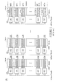
- FIG. 1 is a block diagram illustrating a conventional multi-bank flash memory device 100 having read-while-write capability.
- the flash memory device 100 includes a plurality of banks of flash memory 110A-110C each of which is partitioned into multiple sectors.
- the bank 110A is partitioned into sectors 115a-e
- bank 110B is partitioned into sectors 115f-j
- the bank 110C is partitioned into sectors 115k-o.
- Each of the sectors 115 of the flash memory device 100 has an associated local decoder circuit 105.
- Each of the local decoder circuits 105 is coupled to the associated sector 115 via a plurality of word lines that can be used to access memory cells located within the sector 115.
- the local decoder circuits 105 are activated responsive to address signals provided thereto that indicate which memory cells in the memory are to be accessed.
- the address signals provided to the local decoder circuits 105 can indicate which of the banks 110A-110C, and which of the sectors 115a-o, and which of the plurality word lines corresponding to the memory cells identified by the address signals are to be accessed during a memory read or write operation.
- the multi-bank device 100 is capable of performing a read or write operation in one of the banks while another read or write operation is conducted in another bank simultaneously. For example, a write operation may be performed to memory cells in sector 115a while a read operation is simultaneously carried out in sector 115o.
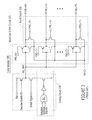
- FIG 2 is a schematic diagram illustrating the local decoder circuit 105 shown in Figure 1.
- the local decoder circuit 105 includes a combinatorial logic circuit 210 that further includes a NAND gate 201 that receives selected ones of the address signals that indicate which memory cells are to be accessed during a read or write operation. This is sometimes referred to as "decoding the address.”
- the word line WL DRV coupled to a word line driver circuit 220 is pulled low when a select signal is asserted.
- the word line driver circuit 220 activates one of the word lines WL ⁇ 7:0> based on a plurality of word line select signals PWL ⁇ 7:0>.
- a decoder Enable signal can be used to provide a supply voltage V PX to the word line prior to or subsequent to a memory operation as a reset.
- the word line select signals PWL ⁇ 7:0> can be provided to the local decoder circuit 105 with the address signals, wherein one of the word line select signals PWL ⁇ 7:0> is activated and the remainder of the word line select signals PWL ⁇ 7:0> are deactivated.
- the portion of the word line driver circuit 220 that is responsive to the activated word line select signal PWL ⁇ 7:0> activates the word line WL ⁇ 7:0> that is coupled thereto.
- the local decoder circuit 105 also includes a reset circuit 230 that can insure that the remaining word lines WL (i.e., the word lines that are not selected) remain in the off state. The read or write operation can thereby be carried out to addresses memory cells.
- combinatorial logic circuitry is included in the local decoder circuits of the conventional flash memory devices. This makes the local decoder circuits to occupy correspondingly large areas in the memory circuit design.
- the invention solves this problem by providing a flash memory device according to the features of claim 1 or 6. Further advantageous embodiments of the invention are mentioned in the subclaims.
- Embodiments according to the invention can provide multi-bank flash memory devices with local row decoder circuits having separate read and write control lines provided thereto.
- a flash memory device can include a local row decoder circuit that is configured to drive word lines coupled to a bank of a flash memory responsive to separate read and write control signals provided thereto from outside the local row decoder circuit.
- Multiple local row decoder circuits can, therefore, be controlled by a single global row decoder circuit that provides the separate read and write control signals to each of the local row decoder circuits.
- the local row decoder circuits may have reduced size, thereby allowing further reductions in the size of the flash memory device.
- a NAND logic circuit used for address decoding is located in the global row decoder circuit, thereby allowing the area allocated to the local row decoder circuit to be reduced.
- the total size of the flash memory may be reduced.
- the flash memory can include a global row decoder circuit that is coupled to the local row decoder circuit via the separate read and write control signals.
- the global row decoder circuit is configured to activate the separate read and write control signals based on an address provided to the global row decoder circuit that indicates memory cells associated with the address are accessed using the word lines.
- the flash memory can include a second local row decoder circuit that is configured drive to a second bank of the flash memory, separate from the first bank, via second word lines that are separate from the first word lines.
- the second local row decoder circuit can be coupled to the global decoder circuit by the separate read and write control signals.
- the global row decoder circuit is configured to activate the first and second local row decoder circuits using the separate read and write control signals.
- the local row decoder circuit and the global row decoder circuit are spaced apart within the flash memory.
- the global row decoder circuit can include a read address decoder circuit that is configured to activate the read control signal coupled to the first and second separate banks based on a read address provided thereto.
- the global row decoder circuit can further include a write address decoder circuit that is configured to activate the write control signal coupled to the first and second separate banks based on a write address provided thereto.
- the local row decoder circuit can include first and second bank select circuits configured to pass the separate read and write control signals to a plurality of word line drivers coupled to a sector within the bank.
- the first and second bank select circuits can include at least one totem-pole arrangement of first and second transistors. The first and second transistors can be made conductive to pass at least one of the separate read and write control signals to the plurality of word line drivers associated with the sector responsive to at least one select signal that indicates the local row decoder circuit is coupled to the bank that includes a memory location corresponding to a write or read address provided to the global decoder circuit.
- the first and second bank select circuits can include at least one pass transistor that is configured to pass at least one of the separate read and write control signals to the plurality of word line drivers responsive to at least one bank select signal that indicates that the bank to which the local row decoder circuit is coupled includes a memory location corresponding to an address provided to the flash memory.
- the global row decoder circuit can include first and second NAND combinatorial logic circuits or first and second NOR combinatorial logic circuits configured to provide the separate read and write control signals.
- the first and second NAND combinatorial logic circuits or the first and second NOR combinatorial logic circuits are configured to activate responsive to a read address for a read operation or a write address for a write operation respectively.
- the flash memory device can further include a second bank of the flash memory that is configured to perform a read operation addressed thereto via a second local row decoder circuit simultaneous with the write operation.
- the flash memory has read-while-write capability that can include an ability to perform a write operation in the first bank of the flash memory via the first local row decoder circuit while simultaneously performing a read operation in a second bank of the flash memory via another local row decoder circuit.
- the flash memory has read-while-write capability that can include an ability to perform a first read or write operation in a first sector of the bank while simultaneously performing a second read or write operation in a second sector of the bank that is separate from the first sector via another local row decoder circuit.
- Embodiments according to the invention can provide local row decoder circuits that are configured to drive word lines for associated sectors of the flash memory device.
- the local row decoder circuits can be activated by separate read and write control signals that are provided from outside the local row decoder circuit, such as from a global row decoder circuit.
- Multiple local row decoder circuits can, therefore, be controlled by a single global row decoder circuit that provides the separate read and write control signals to each of the local row decoder circuits under its control.
- the local row decoder circuits may occupy less area, thereby allowing further reductions in the size of the flash memory device.
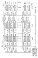
- FIG. 3 is a block diagram that illustrates embodiments of multi-bank flash memory devices having read-while-write capability according to the invention.
- a multi-bank flash memory device 300 includes a plurality of banks 301A-301C that are organized as sectors.
- each of the banks 301A-301C is defined to include sectors 315a-e, 315f-j, and 315k-o, respectively.
- Each of the sectors in the banks is coupled to an associated local row decoder circuit 305 by a plurality of word lines coupled to memory cells within the sectors.
- the local row decoder circuit 305 is coupled to the sector 315a by a plurality of word lines 318.
- Selected ones of the local row decoder circuits 305 are coupled to ones of global row decoder circuits 310 by separate global read and write control lines that conduct global read and write control signals to the selected ones of the local row decoder circuits 305.
- the sectors that operate under the control of the global row decoder circuit 310 (via the respective local row decoder circuit coupled thereto) are organized into MAT portions of the respective banks of the flash memory.
- the local row decoder circuits 305 operate under the control of the global row decoder circuit 310.
- a write operation that is addressed to memory cells in sector 315a is carried out via local row decoder circuit 305 under the control of the global row decoder circuit 310 by asserting the global write control signal to all of the local row decoder circuits 305 coupled to the global write control line.
- the address signals provided for the write operation do not identify memory cells located within sectors 315f or 315k, the write operation is not carried out in those sectors.
- the write operation when, for example, a write operation is to be performed to memory cells located in a sector of the flash memory under the control of the global row decoder circuit, the write operation will be carried in one of the sectors included in the MAT portion associated with the global row decoder circuit.
- multi-bank flash memory devices have read-while-write capability, wherein a read operation can be performed in one of the sectors in a MAT portion of the flash memory while a write operation is simultaneously performed in another sector within the same MAT portion.
- a read operation can be performed in section 315a while a write operation is simultaneously performed in section 315k under the control of the global row decoder circuit 310.
- the different MAT portions of the multi-bank flash memory device 300 can operate independently from one another. For example, a write operation can be performed in a sector included in a first one of the MAT portions while a second write operation is performed in a sector included in a second MAT portion of the flash memory device.
- Figure 3 illustrates a variable number N of banks of flash memory.
- the banks can be further organized into a variable number m of MAT portions.
- Each of the m MAT portions of the banks has an associated global row decoder circuit 310 that controls the operation of the local row decoder circuits 305 associated with each of the sectors include in the m MAT portions.
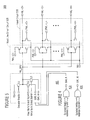
- Figure 4 is a schematic diagram illustrating embodiments of combinatorial logic circuits included in global row decoder circuits according to the invention.
- the global row decoder circuit 400 includes separate combinatorial logic circuits 410 and 420 that generate separate read and write control signals respectively.
- the combinatorial logic circuit 410 is responsive to selected read address signals to provide the global read control signal to the local row decoder circuits that operate under the control of the global row decoder circuit 400.
- the combinatorial logic circuit 420 is responsive to selected write address signals to provide the global write control signal to the local row decoder circuits that operate under the control of the global row decoder circuit 400.
- each of the global row decoder circuits 310 receives read and write address signals and is configured to determine whether the address signals provided thereto correspond to memory locations that are coupled to the local row decoder circuits 305 that operate under the global row decoder circuit's 310 control.
- the read and write address signals that are selectively provided to the combinatorial logic circuits included in the remaining global row decoder circuits can be different based on which of the sectors of the flash memory device are to be accessed via the remaining global row decoder circuits.
- the combinatorial logic circuits can be NAND logic circuits (or gates) as shown in Figure 4. In other embodiments according to the invention, the combinatorial logic circuits can be logical NOR gates. Other types of combinatorial logic circuits may be used.
- FIG. 5 is a schematic diagram that illustrates embodiments of bank select circuits according to the invention.
- a bank select circuit 510 includes pass transistors 512 and 513 that can be made conductive (i.e., turned on) responsive to separate read and write bank select signals, respectively.
- the pass transistors 512 and 513 can be turned on to pass the global read and write control signals GWL R and GWL W, respectively, to a word line driver line as a word line driver signal WL DRV.
- a transistor 511 can be made nonconductive (i.e., turned off) responsive to a high going decoder enable signal to buffer the word line driver signal WL DRV from a supply voltage V PX .
- the supply voltage V PX can otherwise be used to provide an initialization voltage on the word line driver line prior to or subsequent to a memory operation.
- the separate read or write control signals are provided to a word line driver circuit 520 that enables a selected word line WL coupled to the sector associated with the local row decoder circuit.
- the word line driver circuit 520 further includes a plurality of sections that each drive one of the word lines coupled to memory cells in the sector. Each of the sections includes a totem pole arrangement, of upper and lower transistors, that drives the associated word line WL.
- the word line WL to be driven by the word line driver circuit 520 is selected based on a set of word line select signals that are provided to each of the sections of the word line driver circuit 520.
- a reset circuit 530 is coupled to each of the word lines WL driven by sections of the word line driver circuit 520 and operates to reset the voltage on each of the word lines WL prior or subsequent to a memory operation based on a word line reset signal, which can, in some embodiments according to the invention, be an inverted form of the word select signals.
- the word line select signals indicate which of the totem pole circuits included in sections of the word line driver circuit 520 is to drive the associated word line WL.
- each of the totem pole circuits included in the word line driver circuit 520 receives the read or write control signal provided by the bank select circuit 510.
- the read or write control signal causes each of the upper transistors in the totem pole circuits to become conductive, thereby passing the respective word line select signal PWL that is coupled to the totem pole circuit to the associated word line WL. Therefore, each of the totem pole circuits passes the associated word line select signal to the word line WL at the output of the totem pole circuit to activate the word line selected by the word line select signals.
- word lines word lines, word line select signals, and word line reset signals
- embodiments according to the invention may utilize a plurality of these signals.
- eight word lines are coupled to each sector.
- Such embodiments can, therefore, utilize eight word line select signals and eight word line reset signals.
- Other numbers of word lines, word line select signals, and word line reset signals can be utilized in embodiments according to the invention.
- FIG. 6 is a circuit diagram illustrating embodiments of local row decoder circuits according to the invention.
- a local row decoder circuit 605 includes a totem pole arrangement of transistors for each of the separate read and write control signals provided to a word line driver circuit 620.
- the totem pole arrangement includes upper and lower transistors 612 and 613, respectively, and is responsive to a read bank select signal to pass the read control signal to the word line drive circuit 620 during a read operation.
- the totem pole arrangement of transistors 614 and 615 operates in response to a write bank select signal that causes transistor 614 to become conductive to pass the write control signal to the word line driver circuit 620 during a write operation.
- the word line driver circuit 620 drives the word line WL that is selected by the word line select signals.
- the local row decoder circuit 600 further includes a reset circuit 630 that can be used to reset the voltage on each of the word lines WL responsive to a word line reset signal, which can in some embodiments according to the invention, be an inverted version of the word line select signals.
- embodiments according to the invention can provide local row decoder circuits that are free of combinatorial type logic circuits that otherwise may occupy large areas in each of the local row decoder circuits as characterized in the prior art.
- the combinatorial type logic circuits used to provide address decoding is instead included in the global row decoder circuit that controls selected ones of the local row decoder circuits using separate read and write control lines provided thereto. Accordingly, the combinatorial type logic circuits that occupy large areas can be located in the global row decoder circuit that controls multiple ones of the row decoder circuits that are coupled to sectors of the flash memory.
Landscapes
- Engineering & Computer Science (AREA)
- Microelectronics & Electronic Packaging (AREA)
- Read Only Memory (AREA)
- Non-Volatile Memory (AREA)
Abstract
Description
Claims (18)
- A flash memory device, characterized by:a local row decoder circuit configured to drive word lines coupled to a flash memory bank responsive to separate read and write control signals provided thereto from outside the local row decoder circuit.
- A flash memory device according to Claim 1, wherein the flash memory device supports read-while-write capability wherein a read operation in a first bank of the flash memory device can be carried out simultaneous with a write operation in a second bank of the flash memory device.
- A flash memory device according to Claim 1 or 2, further comprising:a global row decoder circuit, coupled to the local row decoder circuit via the separate read and write control signals, and configured to activate the separate read and write control signals based on an address provided to the global row decoder circuit that indicates memory cells associated with the address are accessed using the word lines.
- A flash memory device according to Claim 3, wherein
the local row decoder circuit comprises a first local row decoder circuit, the bank comprises a first bank, and the word lines comprise first word lines, and
the flash memory device further comprises a second local row decoder circuit configured to drive a second bank of the flash memory device, separate from the first bank, via second word lines that are separate from the first word lines, wherein the second local row decoder circuit is coupled to the global decoder circuit by the separate read and write control signals. - A flash memory device according to Claim 4, wherein the global row decoder circuit is configured to activate the first and second local row decoder circuits using the separate read and write control signals.
- A flash memory device having read-while-write capability comprising:characterized by:a plurality of banks of a flash memory;a plurality of local row decoder circuits configured to drive a plurality of word lines coupled to a respective sector in each of the plurality of banks; anda global row decoder circuit configured to provide separate write and read control signals to each of the plurality of local row decoder circuits to enable a read operation in a first sector in one of the plurality of banks and enable a write operation in a second sector in another of the plurality of banks simultaneous with the read operation.
- A flash memory device according to Claim 6, wherein the global row decoder circuit is coupled to the plurality of local row decoder circuits via the separate read and write control signals, and configured to determine whether to activate the separate read and write control signals based on an address for the read or write operation provided to the global row decoder circuit.
- A flash memory device according to any of Claims 3 to 7, wherein the plurality of local row decoder circuits and the global row decoder circuit are spaced apart within the flash memory.
- A flash memory device according to any of Claims 4 to 8, wherein the global row decoder circuit comprises:a read address decoder circuit configured to activate the read control signal coupled to the first and second separate banks based on a read address provided thereto; anda write address decoder circuit configured to activate the write control signal coupled to the first and second separate banks based on a write address provided thereto.
- A flash memory device according to Claim 9, wherein the read address decoder circuit and the write address decoder circuit are configured to be active simultaneously.
- A flash memory device according to any of Claims 1 to 10, wherein the local row decoder circuit comprises first and second bank select circuits configured to pass the separate read and write control signals to a plurality of word line drivers coupled to a sector within the bank.
- A flash memory device according to Claim 11, wherein the first and second bank select circuits comprise at least one totem-pole arrangement of first and second transistors wherein the first and second transistors are conductive to pass at least one of the separate read and write control signals to the plurality of word line drivers associated with the sector responsive to at least one select signal that indicates the local row decoder circuit is coupled to the bank that includes a memory location corresponding to a write or read address provided to the global decoder circuit.
- A flash memory device according to Claim 11 or 12, wherein the first and second bank select circuits comprise at least one pass transistor configured to pass at least one of the separate read and write control signals to the plurality of word line drivers responsive to at least one bank select signal that indicates that the bank to which the local row decoder circuit is coupled includes a memory location corresponding to an address provided to the flash memory.
- A flash memory device according to any of Claims 3 to 13, wherein the global row decoder circuit comprises first and second NAND combinatorial logic circuits or first and second NOR combinatorial logic circuits configured to provide the separate read and write control signals.
- A flash memory device according to Claim 14, wherein the first and second NAND combinatorial logic circuits or the first and second NOR combinatorial logic circuits are configured to activate responsive to a read address for a read operation or a write address for a write operation respectively.
- A flash memory device according to any of Claims 1 to 15, wherein the flash memory bank comprises a first bank configured to perform a write operation addressed to the first bank via the local row decoder circuit, and a second bank configured to perform a read operation addressed thereto via a second local row decoder circuit simultaneous with the write operation.
- A flash memory device according to any of Claims 1 to 16, wherein the flash memory bank comprises a first bank, and the flash memory device has read-while-write capability comprising an ability to perform a write operation in the first bank via the first local row decoder circuit while simultaneously performing a read operation in a second bank of the flash memory device via another local row decoder circuit.
- A flash memory device according to any of Claims 1 to 17, wherein the flash memory device has read-while-write capability comprising an ability to perform a first read or write operation in a first sector of the bank while simultaneously performing a second read or write operation in a second sector of the bank that is separate from the first sector via another local row decoder circuit.
Applications Claiming Priority (2)
| Application Number | Priority Date | Filing Date | Title |
|---|---|---|---|
| KR10-2002-0048045A KR100481857B1 (en) | 2002-08-14 | 2002-08-14 | Flash memory device having decoder to reduce chip area and to implement independent operation of each bank |
| KR2002048045 | 2002-08-14 |
Publications (2)
| Publication Number | Publication Date |
|---|---|
| EP1389781A2 true EP1389781A2 (en) | 2004-02-18 |
| EP1389781A3 EP1389781A3 (en) | 2006-02-08 |
Family
ID=30768216
Family Applications (1)
| Application Number | Title | Priority Date | Filing Date |
|---|---|---|---|
| EP03017907A Withdrawn EP1389781A3 (en) | 2002-08-14 | 2003-08-06 | Flash memory device having local decoder circuitry |
Country Status (5)
| Country | Link |
|---|---|
| US (1) | US7079417B2 (en) |
| EP (1) | EP1389781A3 (en) |
| JP (1) | JP4452463B2 (en) |
| KR (1) | KR100481857B1 (en) |
| CN (1) | CN100520974C (en) |
Families Citing this family (44)
| Publication number | Priority date | Publication date | Assignee | Title |
|---|---|---|---|---|
| KR100622349B1 (en) * | 2004-08-04 | 2006-09-14 | 삼성전자주식회사 | A method for managing a defective block in a flash memory device and a flash memory device having a defective block management function. |
| KR100645046B1 (en) * | 2004-10-07 | 2006-11-10 | 삼성전자주식회사 | Row decoder circuit of nonvolatile memory device |
| KR100664866B1 (en) * | 2005-04-26 | 2007-01-03 | 매그나칩 반도체 유한회사 | Address decoder circuit |
| US7242623B2 (en) | 2005-07-12 | 2007-07-10 | Infineon Technologies Flash Gmbh & Co. Kg | Non-volatile memory cell device, programming element and method for programming data into a plurality of non-volatile memory cells |
| US7260019B1 (en) | 2005-10-31 | 2007-08-21 | Spansion Llc | Memory array |
| US20070165479A1 (en) * | 2006-01-17 | 2007-07-19 | Norbert Rehm | Local wordline driver scheme to avoid fails due to floating wordline in a segmented wordline driver scheme |
| KR100704039B1 (en) * | 2006-01-20 | 2007-04-04 | 삼성전자주식회사 | Semiconductor memory device in which the decoded signal is bused in the word line direction |
| US7633828B2 (en) * | 2006-07-31 | 2009-12-15 | Sandisk 3D Llc | Hierarchical bit line bias bus for block selectable memory array |
| US8279704B2 (en) | 2006-07-31 | 2012-10-02 | Sandisk 3D Llc | Decoder circuitry providing forward and reverse modes of memory array operation and method for biasing same |
| US7596050B2 (en) * | 2006-07-31 | 2009-09-29 | Sandisk 3D Llc | Method for using a hierarchical bit line bias bus for block selectable memory array |
| US7499366B2 (en) | 2006-07-31 | 2009-03-03 | Sandisk 3D Llc | Method for using dual data-dependent busses for coupling read/write circuits to a memory array |
| EP2062264B1 (en) * | 2006-07-31 | 2015-10-07 | Sandisk 3D LLC | Method and apparatus for memory array incorporating two data busses for memory array block selection |
| US7570523B2 (en) * | 2006-07-31 | 2009-08-04 | Sandisk 3D Llc | Method for using two data busses for memory array block selection |
| US7463536B2 (en) * | 2006-07-31 | 2008-12-09 | Sandisk 3D Llc | Memory array incorporating two data busses for memory array block selection |
| KR100781980B1 (en) * | 2006-11-02 | 2007-12-06 | 삼성전자주식회사 | Decoder in nonvolatile memory device and decoding method thereof |
| KR100915815B1 (en) * | 2007-09-13 | 2009-09-07 | 주식회사 하이닉스반도체 | A semiconductor memory device having a control block sharing a plurality of row decoders |
| US7672163B2 (en) * | 2007-09-14 | 2010-03-02 | Sandisk Corporation | Control gate line architecture |
| JP2009272000A (en) * | 2008-05-07 | 2009-11-19 | Toshiba Microelectronics Corp | Nonvolatile semiconductor memory and its test method |
| KR101360812B1 (en) * | 2008-06-05 | 2014-02-11 | 삼성전자주식회사 | Memory device and memory system having the same |
| TWI393141B (en) * | 2008-09-03 | 2013-04-11 | Elan Microelectronics Corp | A column decoder that can be used to speed up the read speed in a number of programmable flash memories |
| KR20100040580A (en) | 2008-10-10 | 2010-04-20 | 성균관대학교산학협력단 | Stacked memory devices |
| US10867298B1 (en) | 2008-10-31 | 2020-12-15 | Wells Fargo Bank, N.A. | Payment vehicle with on and off function |
| US20100114768A1 (en) | 2008-10-31 | 2010-05-06 | Wachovia Corporation | Payment vehicle with on and off function |
| US8189390B2 (en) * | 2009-03-05 | 2012-05-29 | Mosaid Technologies Incorporated | NAND flash architecture with multi-level row decoding |
| US8645637B2 (en) * | 2010-11-16 | 2014-02-04 | Micron Technology, Inc. | Interruption of write memory operations to provide faster read access in a serial interface memory |
| US8737137B1 (en) | 2013-01-22 | 2014-05-27 | Freescale Semiconductor, Inc. | Flash memory with bias voltage for word line/row driver |
| US11429975B1 (en) | 2015-03-27 | 2022-08-30 | Wells Fargo Bank, N.A. | Token management system |
| US11170364B1 (en) | 2015-07-31 | 2021-11-09 | Wells Fargo Bank, N.A. | Connected payment card systems and methods |
| US10992679B1 (en) | 2016-07-01 | 2021-04-27 | Wells Fargo Bank, N.A. | Access control tower |
| US11935020B1 (en) | 2016-07-01 | 2024-03-19 | Wells Fargo Bank, N.A. | Control tower for prospective transactions |
| US12130937B1 (en) | 2016-07-01 | 2024-10-29 | Wells Fargo Bank, N.A. | Control tower for prospective transactions |
| US11615402B1 (en) | 2016-07-01 | 2023-03-28 | Wells Fargo Bank, N.A. | Access control tower |
| US11386223B1 (en) | 2016-07-01 | 2022-07-12 | Wells Fargo Bank, N.A. | Access control tower |
| US11886611B1 (en) | 2016-07-01 | 2024-01-30 | Wells Fargo Bank, N.A. | Control tower for virtual rewards currency |
| US11556936B1 (en) | 2017-04-25 | 2023-01-17 | Wells Fargo Bank, N.A. | System and method for card control |
| US11062388B1 (en) | 2017-07-06 | 2021-07-13 | Wells Fargo Bank, N.A | Data control tower |
| US11188887B1 (en) | 2017-11-20 | 2021-11-30 | Wells Fargo Bank, N.A. | Systems and methods for payment information access management |
| US10482968B1 (en) * | 2018-11-22 | 2019-11-19 | Wuhan Xinxin Semiconductor Manufacturing Co., Ltd. | Local x-decoder and related memory system |
| US10992606B1 (en) | 2020-09-04 | 2021-04-27 | Wells Fargo Bank, N.A. | Synchronous interfacing with unaffiliated networked systems to alter functionality of sets of electronic assets |
| US11546338B1 (en) | 2021-01-05 | 2023-01-03 | Wells Fargo Bank, N.A. | Digital account controls portal and protocols for federated and non-federated systems and devices |
| DE102021107045B4 (en) | 2021-03-10 | 2024-11-21 | Elmos Semiconductor Se | Computer system for an engine control with a program memory and a data memory |
| US11836690B1 (en) | 2022-04-12 | 2023-12-05 | Wells Fargo Bank, N.A. | Systems and methods for private network issuance of digital currency |
| US12155641B1 (en) | 2022-04-15 | 2024-11-26 | Wells Fargo Bank, N.A. | Network access tokens and meta-application programming interfaces for enhanced inter-enterprise system data promulgation and profiling |
| CN115424649B (en) * | 2022-09-15 | 2025-03-28 | 长鑫存储技术有限公司 | Memory and memory operation method |
Family Cites Families (50)
| Publication number | Priority date | Publication date | Assignee | Title |
|---|---|---|---|---|
| US4620299A (en) | 1985-03-04 | 1986-10-28 | Motorola, Inc. | Row decoder |
| US4661724A (en) | 1985-05-06 | 1987-04-28 | Motorola, Inc. | Row decoder |
| JPS6366789A (en) | 1986-09-09 | 1988-03-25 | Mitsubishi Electric Corp | Cmos row decoder circuit |
| JP2525455B2 (en) | 1988-05-30 | 1996-08-21 | 富士通株式会社 | Semiconductor memory device |
| JPH02218096A (en) | 1989-02-17 | 1990-08-30 | Sharp Corp | Row selecting circuit for semiconductor memory |
| US5222040A (en) | 1990-12-11 | 1993-06-22 | Nexcom Technology, Inc. | Single transistor eeprom memory cell |
| KR940005695B1 (en) | 1990-12-19 | 1994-06-22 | 삼성전자 주식회사 | Row decoder circuit of non-volatile memory device |
| JPH04222998A (en) | 1990-12-25 | 1992-08-12 | Nec Corp | Semiconductor memory device |
| JP2835215B2 (en) | 1991-07-25 | 1998-12-14 | 株式会社東芝 | Nonvolatile semiconductor memory device |
| IT1253680B (en) | 1991-08-30 | 1995-08-22 | St Microelectronics Srl | NAND TYPE ROM DECODER |
| US5187394A (en) | 1992-01-13 | 1993-02-16 | Motorola, Inc. | Configurable row decoder driver circuit |
| DE4311358C2 (en) * | 1992-04-07 | 1999-07-22 | Mitsubishi Electric Corp | Non-volatile semiconductor memory device and operating method for a non-volatile semiconductor memory device and method for programming information into a non-volatile semiconductor memory device |
| JP3093432B2 (en) | 1992-04-08 | 2000-10-03 | 日本電気株式会社 | Row decoder |
| US5668485A (en) | 1992-05-21 | 1997-09-16 | Texas Instruments Incorporated | Row decoder with level translator |
| KR960008825B1 (en) | 1993-11-18 | 1996-07-05 | Samsung Electronics Co Ltd | Row redundancy circuit and method of semiconductor memory device with double row decoder |
| US5365479A (en) | 1994-03-03 | 1994-11-15 | National Semiconductor Corp. | Row decoder and driver with switched-bias bulk regions |
| JPH08167285A (en) * | 1994-12-07 | 1996-06-25 | Toshiba Corp | Semiconductor memory device |
| US5696721A (en) | 1995-05-05 | 1997-12-09 | Texas Instruments Incorporated | Dynamic random access memory having row decoder with level translator for driving a word line voltage above and below an operating supply voltage range |
| US5615164A (en) | 1995-06-07 | 1997-03-25 | International Business Machines Corporation | Latched row decoder for a random access memory |
| US5719818A (en) | 1996-04-18 | 1998-02-17 | Waferscale Integration Inc. | Row decoder having triple transistor word line drivers |
| KR100228424B1 (en) | 1996-06-29 | 1999-11-01 | 김영환 | X decoder circuit of semiconductor memory device |
| US5777926A (en) | 1996-10-24 | 1998-07-07 | Programmable Microelectronics Corporation | Row decoder circuit for PMOS non-volatile memory cell which uses channel hot electrons for programming |
| KR100237624B1 (en) | 1996-10-30 | 2000-01-15 | 김영환 | A row decoder |
| KR100250752B1 (en) * | 1996-12-28 | 2000-05-01 | 김영환 | Decoder Circuit in Flash Memory |
| KR100224779B1 (en) | 1996-12-31 | 1999-10-15 | 김영환 | Roo decoder circuit |
| TW405121B (en) | 1996-12-31 | 2000-09-11 | Hyundai Electronics Ind | Sub row decoder circuit for semiconductor memory device |
| US5796656A (en) | 1997-02-22 | 1998-08-18 | Programmable Microelectronics Corporation | Row decoder circuit for PMOS non-volatile memory cell which uses electron tunneling for programming and erasing |
| KR100254565B1 (en) * | 1997-08-28 | 2000-05-01 | 윤종용 | Row decoder circuit of flash memory device having divided word line structure |
| US5886923A (en) * | 1997-10-27 | 1999-03-23 | Integrated Silicon Solution Inc. | Local row decoder for sector-erase fowler-nordheim tunneling based flash memory |
| US6055203A (en) | 1997-11-19 | 2000-04-25 | Waferscale Integration | Row decoder |
| DE69739922D1 (en) | 1997-11-26 | 2010-08-12 | St Microelectronics Srl | Row decoder for flash EEPROM memory array with the possibility of selective deletion of a subset of rows of a sector |
| KR100744103B1 (en) * | 1997-12-30 | 2007-12-20 | 주식회사 하이닉스반도체 | Low Decoder for Flash Memory Devices |
| EP0928003B1 (en) | 1997-12-31 | 2005-09-21 | STMicroelectronics S.r.l. | Row decoder circuit for an electronic memory device, particularly for low voltage applications |
| US5999479A (en) | 1998-01-21 | 1999-12-07 | Integrated Silicon Solution, Inc. | Row decoder for nonvolatile memory having a low-voltage power supply |
| US6118726A (en) | 1998-02-02 | 2000-09-12 | International Business Machines Corporation | Shared row decoder |
| US5991198A (en) | 1998-04-02 | 1999-11-23 | Nexflash Technologies, Inc. | Local row decoder and associated control logic for fowler-nordheim tunneling based flash memory |
| US6285360B1 (en) | 1998-05-08 | 2001-09-04 | Aurora Systems, Inc. | Redundant row decoder |
| DE19928454B4 (en) | 1998-06-29 | 2010-01-21 | Fujitsu Microelectronics Ltd. | Memory device with row decoder |
| US6044020A (en) | 1998-07-28 | 2000-03-28 | Samsung Electronics Co., Ltd. | Nonvolatile semiconductor memory device with a row decoder circuit |
| JP2000268561A (en) * | 1999-03-18 | 2000-09-29 | Toshiba Microelectronics Corp | Semiconductor storage device |
| KR100297725B1 (en) | 1999-04-23 | 2001-10-29 | 윤종용 | Row decoder driver of semiconductor memory device |
| US6377502B1 (en) * | 1999-05-10 | 2002-04-23 | Kabushiki Kaisha Toshiba | Semiconductor device that enables simultaneous read and write/erase operation |
| EP1061525B1 (en) | 1999-06-17 | 2006-03-08 | STMicroelectronics S.r.l. | Row decoder for a nonvolatile memory with possibility of selectively biasing word lines to positive or negative voltages |
| KR100308480B1 (en) * | 1999-07-13 | 2001-11-01 | 윤종용 | Flash memory device with row decoding structure which is appropriate for high desitty |
| US6278297B1 (en) | 1999-09-14 | 2001-08-21 | Texas Instruments Incorporated | Row decoder with switched power supply |
| US6772273B1 (en) * | 2000-06-29 | 2004-08-03 | Intel Corporation | Block-level read while write method and apparatus |
| TW540053B (en) * | 2000-07-13 | 2003-07-01 | Samsung Electronics Co Ltd | Row decoder of a NOR-type flash memory device |
| JP4503809B2 (en) | 2000-10-31 | 2010-07-14 | 株式会社東芝 | Semiconductor memory device |
| US6426914B1 (en) | 2001-04-20 | 2002-07-30 | International Business Machines Corporation | Floating wordline using a dynamic row decoder and bitline VDD precharge |
| KR100418521B1 (en) * | 2001-06-11 | 2004-02-11 | 삼성전자주식회사 | non-volatile semiconductor memory devices having hierarchical sector structure |
-
2002
- 2002-08-14 KR KR10-2002-0048045A patent/KR100481857B1/en not_active Expired - Fee Related
-
2003
- 2003-07-18 US US10/622,278 patent/US7079417B2/en not_active Expired - Lifetime
- 2003-08-05 JP JP2003286360A patent/JP4452463B2/en not_active Expired - Fee Related
- 2003-08-06 EP EP03017907A patent/EP1389781A3/en not_active Withdrawn
- 2003-08-14 CN CNB031540384A patent/CN100520974C/en not_active Expired - Lifetime
Also Published As
| Publication number | Publication date |
|---|---|
| KR20040015901A (en) | 2004-02-21 |
| CN1484251A (en) | 2004-03-24 |
| JP4452463B2 (en) | 2010-04-21 |
| CN100520974C (en) | 2009-07-29 |
| JP2004079161A (en) | 2004-03-11 |
| KR100481857B1 (en) | 2005-04-11 |
| US20040090825A1 (en) | 2004-05-13 |
| EP1389781A3 (en) | 2006-02-08 |
| US7079417B2 (en) | 2006-07-18 |
Similar Documents
| Publication | Publication Date | Title |
|---|---|---|
| EP1389781A2 (en) | Flash memory device having local decoder circuitry | |
| JP3351595B2 (en) | Semiconductor memory device | |
| US8854884B2 (en) | NAND flash architecture with multi-level row decoding | |
| US9330765B2 (en) | Non-volatile memory device having configurable page size | |
| US8072816B2 (en) | Memory block reallocation in a flash memory device | |
| US5898637A (en) | System and method for selecting shorted wordlines of an array having dual wordline drivers | |
| US20050281122A1 (en) | Memory system, method and predecoding circuit operable in different modes for selectively accessing multiple blocks of memory cells for simultaneous writing or erasure | |
| EP1063652A2 (en) | Flash memory with alterable erase sector size | |
| JPH0628889A (en) | Flash memory device provided with column redundancy, method for addressing to above device and preliminary adjusting method of above memory device | |
| KR20020083409A (en) | Flash memory capable of changing bank configuration | |
| US20090016143A1 (en) | Word line activation in memory devices | |
| JP2540028B2 (en) | Integrated programming circuit | |
| US8971129B2 (en) | NROM device with reduced power unit | |
| JPH07201193A (en) | 2-line address decoding / selection circuit | |
| JP4633958B2 (en) | Nonvolatile semiconductor memory | |
| JP4757978B2 (en) | Nonvolatile memory device | |
| US6055203A (en) | Row decoder | |
| US6400622B1 (en) | Semiconductor memory device | |
| JP7157785B2 (en) | Row Redundancy Using Distributed Sectors | |
| US7009910B2 (en) | Semiconductor memory having a flexible dual-bank architecture with improved row decoding | |
| US6704241B1 (en) | Memory architecture with vertical and horizontal row decoding | |
| JP3906112B2 (en) | Semiconductor memory device | |
| JP2000149579A (en) | Semiconductor device having flash memory array | |
| JP2005310246A (en) | Semiconductor memory device | |
| JP2002093191A (en) | Semiconductor storage device |
Legal Events
| Date | Code | Title | Description |
|---|---|---|---|
| PUAI | Public reference made under article 153(3) epc to a published international application that has entered the european phase |
Free format text: ORIGINAL CODE: 0009012 |
|
| AK | Designated contracting states |
Kind code of ref document: A2 Designated state(s): AT BE BG CH CY CZ DE DK EE ES FI FR GB GR HU IE IT LI LU MC NL PT RO SE SI SK TR |
|
| AX | Request for extension of the european patent |
Extension state: AL LT LV MK |
|
| PUAL | Search report despatched |
Free format text: ORIGINAL CODE: 0009013 |
|
| AK | Designated contracting states |
Kind code of ref document: A3 Designated state(s): AT BE BG CH CY CZ DE DK EE ES FI FR GB GR HU IE IT LI LU MC NL PT RO SE SI SK TR |
|
| AX | Request for extension of the european patent |
Extension state: AL LT LV MK |
|
| 17P | Request for examination filed |
Effective date: 20060623 |
|
| AKX | Designation fees paid |
Designated state(s): DE FR GB |
|
| 17Q | First examination report despatched |
Effective date: 20071123 |
|
| RAP1 | Party data changed (applicant data changed or rights of an application transferred) |
Owner name: SAMSUNG ELECTRONICS CO., LTD. |
|
| GRAP | Despatch of communication of intention to grant a patent |
Free format text: ORIGINAL CODE: EPIDOSNIGR1 |
|
| RIC1 | Information provided on ipc code assigned before grant |
Ipc: G11C 8/10 20060101ALI20151103BHEP Ipc: G11C 8/12 20060101ALI20151103BHEP Ipc: G11C 16/08 20060101AFI20151103BHEP |
|
| INTG | Intention to grant announced |
Effective date: 20151124 |
|
| RIN1 | Information on inventor provided before grant (corrected) |
Inventor name: NAM, GA PYO, 151-1904,JUGONG 1 DANJI Inventor name: LEE, SEUNG KEUN |
|
| STAA | Information on the status of an ep patent application or granted ep patent |
Free format text: STATUS: THE APPLICATION IS DEEMED TO BE WITHDRAWN |
|
| 18D | Application deemed to be withdrawn |
Effective date: 20160405 |