EP1388876A1 - Partition wall forming method for plasma display panels using sandblast - Google Patents
Partition wall forming method for plasma display panels using sandblast Download PDFInfo
- Publication number
- EP1388876A1 EP1388876A1 EP02714448A EP02714448A EP1388876A1 EP 1388876 A1 EP1388876 A1 EP 1388876A1 EP 02714448 A EP02714448 A EP 02714448A EP 02714448 A EP02714448 A EP 02714448A EP 1388876 A1 EP1388876 A1 EP 1388876A1
- Authority
- EP
- European Patent Office
- Prior art keywords
- mask
- pattern
- display area
- plasma display
- partition
- Prior art date
- Legal status (The legal status is an assumption and is not a legal conclusion. Google has not performed a legal analysis and makes no representation as to the accuracy of the status listed.)
- Withdrawn
Links
Images




Classifications
-
- H—ELECTRICITY
- H01—ELECTRIC ELEMENTS
- H01J—ELECTRIC DISCHARGE TUBES OR DISCHARGE LAMPS
- H01J9/00—Apparatus or processes specially adapted for the manufacture, installation, removal, maintenance of electric discharge tubes, discharge lamps, or parts thereof; Recovery of material from discharge tubes or lamps
- H01J9/24—Manufacture or joining of vessels, leading-in conductors or bases
-
- H—ELECTRICITY
- H01—ELECTRIC ELEMENTS
- H01J—ELECTRIC DISCHARGE TUBES OR DISCHARGE LAMPS
- H01J9/00—Apparatus or processes specially adapted for the manufacture, installation, removal, maintenance of electric discharge tubes, discharge lamps, or parts thereof; Recovery of material from discharge tubes or lamps
- H01J9/24—Manufacture or joining of vessels, leading-in conductors or bases
- H01J9/241—Manufacture or joining of vessels, leading-in conductors or bases the vessel being for a flat panel display
- H01J9/242—Spacers between faceplate and backplate
-
- H—ELECTRICITY
- H01—ELECTRIC ELEMENTS
- H01J—ELECTRIC DISCHARGE TUBES OR DISCHARGE LAMPS
- H01J11/00—Gas-filled discharge tubes with alternating current induction of the discharge, e.g. alternating current plasma display panels [AC-PDP]; Gas-filled discharge tubes without any main electrode inside the vessel; Gas-filled discharge tubes with at least one main electrode outside the vessel
- H01J11/10—AC-PDPs with at least one main electrode being out of contact with the plasma
- H01J11/12—AC-PDPs with at least one main electrode being out of contact with the plasma with main electrodes provided on both sides of the discharge space
-
- H—ELECTRICITY
- H01—ELECTRIC ELEMENTS
- H01J—ELECTRIC DISCHARGE TUBES OR DISCHARGE LAMPS
- H01J11/00—Gas-filled discharge tubes with alternating current induction of the discharge, e.g. alternating current plasma display panels [AC-PDP]; Gas-filled discharge tubes without any main electrode inside the vessel; Gas-filled discharge tubes with at least one main electrode outside the vessel
- H01J11/20—Constructional details
- H01J11/34—Vessels, containers or parts thereof, e.g. substrates
- H01J11/36—Spacers, barriers, ribs, partitions or the like
-
- H—ELECTRICITY
- H01—ELECTRIC ELEMENTS
- H01J—ELECTRIC DISCHARGE TUBES OR DISCHARGE LAMPS
- H01J2211/00—Plasma display panels with alternate current induction of the discharge, e.g. AC-PDPs
- H01J2211/20—Constructional details
- H01J2211/34—Vessels, containers or parts thereof, e.g. substrates
- H01J2211/36—Spacers, barriers, ribs, partitions or the like
- H01J2211/361—Spacers, barriers, ribs, partitions or the like characterized by the shape
- H01J2211/365—Pattern of the spacers
-
- H—ELECTRICITY
- H01—ELECTRIC ELEMENTS
- H01J—ELECTRIC DISCHARGE TUBES OR DISCHARGE LAMPS
- H01J2211/00—Plasma display panels with alternate current induction of the discharge, e.g. AC-PDPs
- H01J2211/20—Constructional details
- H01J2211/34—Vessels, containers or parts thereof, e.g. substrates
- H01J2211/36—Spacers, barriers, ribs, partitions or the like
- H01J2211/368—Dummy spacers, e.g. in a non display region
Definitions
- the present invention is related to a method for forming partitions for manufacturing a plasma display panel (PDP) having partitions in a display area, and the invention can be applied to formation of partition using a sandblasting method.
- PDP plasma display panel
- a surface discharge type PDP that is used for a color display has partitions for preventing discharge interference between neighboring cells.
- a stripe pattern is adopted, a plurality of partitions, each of which having a band-like shape in a plan view, is arranged in the display area.
- a partition (a so-called box rib) having a shape surrounding each cell in a plan view is arranged in the display area.
- a partition is a baked material of low melting point glass and is formed by using a sandblasting method.
- Fig. 12 shows the conventional process of forming a partition.
- the partition pattern shown in Fig. 12 is a stripe pattern.
- the partition is formed by the following steps.
- B A photolithography technique including exposure of the pattern and development of the same is used for forming masks 103 of a pattern corresponding to the partition.
- a cutting material is blown to cut portions of the partition material 102a that are not masked.
- a spray nozzle is moved in a reciprocating manner along the longitudinal direction of the bands of the mask pattern, so that the wide area of the partition material 102a is dug down equally and gradually.
- the masks 103 that are remained on the patterned partition material 102b are removed.
- the partition material 102b is baked so that a partition 112 is obtained. In the baking process, the volume of the partition material 102b is reduced due to dissipation of binder.
- the partition material 102b is scooped out under the mask 103 at ends of the mask 103 in the direction along the movement of the nozzle so that side cuts are formed.
- This is caused by that a part of the cutting material ejected from the nozzle is reflected by the glass substrate 101, meets the cutting material ejected from the nozzle, and has a moving component in parallel with the direction of the nozzle movement so that the cutting material having the components scoop out the ends of the partitions.
- Quantity of the side cuts becomes greater as a cutting speed increases. It is considered to be the reason that a ratio of the above-mentioned component increases when quantity of a cutting material ejected per unit time is increased.
- the above-mentioned component that causes the side cut is referred to as a jet.
- This side cut induces mask exfoliation that is a cause of a pattering deficiency during the cutting stage.
- the side cut prevents the partition 112 from being formed in uniform height.
- the partition material 102b having curved edges as shown in Fig. 12(D) is baked, the edge portions of the partition 112 become higher than other portions as shown in Fig. 12(E). More specifically, concerning a partition having a design value of height of 140 ⁇ m, it has a height of approximately 200 ⁇ m before the baking process. After being baked, the height is reduced to approximately 70%, and the edge portions become higher than the other portions by 30 ⁇ m.
- This phenomenon is called a "projection", and it is caused by that the top portion is free while the bottom portion is restrained from contracting since it is stuck to the glass substrate 101.
- the projection causes insufficient contact between substrates in a PDP assembling process in which a substrate having the partition 112 is put together with another substrate. If the PDP has a gap between the surfaces to contact with each other, the substrates may vibrate locally due to electrostatic attraction when a high frequency driving voltage is applied for a display, resulting in slight operation sound (buzz sound).
- An object of the present invention is to provide a method for forming partitions of the exact pattern and height as designed in a display area without generating any projections that can be obstacles to contact between substrates.
- the partition material when patterning a partition material that is masked partially by blasting a cutting material, the partition material is masked so as to form a sub partition that is connected to a partition in a display area (a main partition) outside the display area, thereby side cuts are generated outside the display area.
- the sub partition is formed as a grid-like pattern so that the side cuts can be generated in wide area for reducing the depth of the side cuts.
- the partition material is masked so that the auxiliary partition for reducing the side cuts of the sub partition is formed outside the sub partition.
- the edge portion of the auxiliary partition is protruded from the display area, the effect of protecting the sub partition in a cutting process is enhanced.
- the auxiliary partition too, the projection is prevented so that no disturbance is generated for contact between the substrates.
- the pattern of the auxiliary partition is made as a ring pattern.
- the ring pattern reduces concentration of stress due to thermal contraction so that the projection hardly occurs.
- a size of the pattern is set less than a predetermined value. Specifically, it is set to 240 ⁇ m or less.
- Fig. 1 is a schematic diagram of a sandblasting apparatus that is used for a method of the present invention.
- the sandblasting apparatus 90 comprises a conveyor 91, four nozzles (also called blast guns) 92, 93, 94 and 95, a flow control block 96, a filter 97, and a cyclone 98.
- the conveyor 91 moves a work that was conveyed into a work room slowly from the left side to the right side in Fig. 1.
- the nozzles 92, 93, 94 and 95 move in a reciprocating manner in the direction perpendicular to the direction of conveying the work.
- the flow control block 96 mixes a cutting material and compressed gas, and the mixture is sent to the nozzles 92, 93, 94 and 95.
- the cutting material is ejected from the tips of the nozzles 92, 93, 94 and 95 to cut away the work. Scattered cutting material is collected together with cuttings and is sent to the filter 97.
- the filter 97 has a role in removing cuttings larger than the cutting material.
- the cyclone 98 separates the cutting material that passed the filter 97 from minute cuttings.
- the cutting material separated by the cyclone 98 is sent to the flow control block 96 for reuse.
- the minute cuttings are sent to a dust collector.
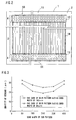
- Fig. 2 is a plan view showing a mask pattern of a first embodiment.
- a partition pattern of the PDP of the first embodiment is a stripe pattern.
- the partition is formed basically in the same manner as the conventional process explained with reference to Fig. 12, which includes patterning a sheet-like partition material 2 that covers the entire surface of a glass substrate 1 that is a panel material by using a sandblasting process, and then baking the partition material 2.
- a mask 30 used for patterning extends over a display area 10 and a non-display area 11 at both sides of the display area 10.
- the display area 10 means an area in which cells are formed on the glass substrate 1, and it corresponds to a display screen of a completed PDP.
- the partition material 2 there are some methods similarly to the conventional process, i.e., a method of applying low melting point glass paste to the glass substrate 1 and drying the same, and a method of sticking a green sheet of low melting point glass onto the glass substrate 1.
- the mask 30 is made of a photo-sensitive resist.
- the glass substrate 1 has a size of 1030 mm x 650 mm for manufacturing a 32-inch PDP.
- a pattern of a portion of the mask 30 to be arranged in the display area 10 (hereinafter referred to as a main mask 3) is a stripe pattern corresponding to the partition to be formed, and it includes straight bands extending along the vertical direction in Fig. 2.
- a pattern of a portion of the mask 30 to be arranged at the outside of the display area 10 (hereinafter referred to as a sub mask 4) is a grid pattern that divides a band-like area 13 along the edge of the display area 10, and it comprises bands corresponding to the pattern of the display area 10 and a plurality of bands perpendicular thereto.
- the sub mask 4 prevents excessive cutting at ends of each band of the stripe pattern. Since the rim of the sub mask 4 is continuous over the entire length in the lateral direction of the display area 10 (i.e., the moving direction for cutting), quantity of the cutting material ejected directly to the edge surface of the sub mask 4 per unit area is less than that in discontinuous case. Thus, the side cuts at the edge surface of the sub mask 4 can be reduced. In addition, thanks to the sub mask 4, the cutting material reflected by the sub mask 4 and the cutting material directly from the nozzle interfere with each other, so that the cutting process is performed equally in the edge portions and the middle portion of the main mask 3.
- partitions can be formed of the exact pattern and height as designed in a display area without any obstruction in contact between the substrates.
- the sub partition arranged at the outside of the display area prevents incomplete contact between the substrates.
- Fig. 3 is a graph showing the relationship between a band width of a mask pattern and quantity of a projection.
- the quantity of a projection depends on the band width of the pattern of the sub mask 4 (sub pattern).
- the band width of the pattern of the main mask 3 main pattern
- the quantity of a projection can be minimized by setting the band width of the sub pattern, i.e., the band width of the partition that is formed in the direction perpendicular to the stripe partition to the value of 240 ⁇ m.
- the band width of the sub pattern By setting the band width of the sub pattern to a value within 160-320 ⁇ m, the projection can be reduced.
- the depth of the side cut is 50 ⁇ m in Fig.
- the quantity of the side cut can be close to zero by using an auxiliary partition or others that will be explained later, so that the quantity of a projection can be reduced to 12 ⁇ m or less when the band width of the sub pattern is set to a value of 240 ⁇ m.
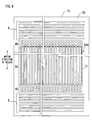
- Fig. 4 is a plan view showing a mask pattern of a second embodiment.
- Fig. 5 is a diagram showing an enlarged part of the mask pattern of the second embodiment.
- the partition pattern is also a stripe pattern.
- the partition is formed in the same way as the first embodiment, which includes patterning a sheet-like partition material 2b that covers the entire surface of a glass substrate 1b by using a sandblasting process and a mask 30b that is a unit of a main mask 3b and a sub mask 4b, and then baking the partition material 2b.
- the second embodiment has three characteristics as follows.
- the auxiliary mask 5 has a role in adjusting the jet in the direction of the nozzle movement so as to reduce the side cuts securely at the portion that is masked by the sub mask 4b.
- Each of the auxiliary masks 5 has a stripe pattern in which seven long bands extend in parallel in the movement direction, and lateral ends of the auxiliary mask 5 protrude from the mask 30b by the length L11. This protrusion enhances the effect of the jet adjustment.
- L1 represents the width of bands except for both ends of the arrangement in the display area 10
- L2 represents the width of the most outside band
- L3 represents the width of bands except for the most outside band in the non-display area 11.
- the nozzle is moved in the vertical direction in Fig. 4 in the cutting process.
- the cutting material is first ejected toward the auxiliary mask 5 located at the upper or the lower non-display area 11, then the cutting material is ejected toward the sub mask 4b, and further the cutting material is ejected toward the main mask 3b. Since the cutting process can be performed faster as the pattern gap of the mask is larger, the cutting action is the largest for the auxiliary mask 5.
- the auxiliary mask 5 has also a function for preventing excessive cutting of the sub mask 4b. If the auxiliary mask 5 is exfoliated and blown off, the sub mask 4b prevents excessive cutting for the main mask 3b.
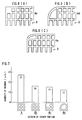
- the corner portion of a sub mask 4c as shown in Fig. 6(A) has a shape of a right-angled rim in which one of squares is filled.
- the corner portion of a sub mask 4d as shown in Fig. 6(B) has an arcuate shape having a radius twice the grid interval.
- the corner portion of a sub mask 4e as shown in Fig. 6(C) has a shape of laterally oblong arc.
- the quantity of a projection depends on a shape of the corner portion.
- the quantity of a projection is less in the arcuate corner portion than in the angled corner portion.
- the quantity of a projection is less in a large radius than in a small radius of the arc. Even the arc of small radius can realize the quantity of a projection of 16 ⁇ m or less that is effective for reducing operational sound.
- it is desirable to set the quantity of a projection to 12 ⁇ m or less.
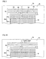
- Fig. 8 is a plan view showing a first variation of an auxiliary mask pattern.
- the pattern of an auxiliary mask 5b is a pattern having three coaxial rings elongated in the lateral direction and consisting of half circles and lines. However, a slit 51a is formed in each half circle at each end of each ring, so the pattern of the auxiliary mask 5b is a discontinuous ring pattern in the strict sense. Since the slit 51a divides the ring, only a part of a ring is blown off if partial mask exfoliation occurs in the cutting process of the entire of one ring, and it is hard to occur that the entire of one ring is blown off.
- the ring pattern is made by connecting both ends of a band with each other in the stripe pattern, and the exfoliation hardly occurs in it compared with the stripe pattern. Since ends of all rings including the most inside ring protrude from the mask 30b, the effect of protecting the mask 30b is enhanced.
- Fig. 9 is a plan view showing a second variation of an auxiliary mask pattern.
- the pattern of the partition mask 3b located at the display area 10 is a mesh pattern.
- An auxiliary mask 5c is positioned at the vicinity of a mask 30c that includes the main mask 3b and the sub mask 4b.
- the pattern of the auxiliary mask 5c is a stripe pattern in which a plurality of bands shorter than the entire length in the lateral direction of the display area 10 is arranged in the moving direction as a plurality of discontinuous lines that are parallel to each other.
- the jet can be controlled by setting the width of the slit 55 that divides the band of the stripe. There is also an effect that a portion that will be blown off is small when mask exfoliation occurs.
- the slits 55 are arranged so that the discontinuous points of plural discontinuous lines are shifted from each other, and thereby the jet is prevented from being enhanced locally in the sub mask 4b.
- the both ends of the auxiliary mask 5c protrude from the mask 30b by the length L11.
- the band closest to the mask 30b among bands constituting the stripe pattern is not protruded from the mask 30b.
- the reason thereof is to make the exfoliation of a band that will contribute to the protection of the mask 30b most hard to happen. If this band is exfoliated at early stage, quantity of side cut of the sub partition increases compared with the case where other bands are exfoliated. Since the ends of the band are not protruded from the mask 30b, jet pressure will be weaken at the end of the band.
- the shape of the band that is closest to the mask 30b can be adopted also for the auxiliary mask of the embodiment as shown in Fig. 5.
- Fig. 10 is a plan view showing a third variation of an auxiliary mask pattern.
- the partition pattern is a mesh pattern.
- the pattern of an auxiliary mask 5d is a stripe pattern in which a plurality of bands sufficiently shorter than the entire length in the moving direction of the display area 10 is arranged in the moving direction as a plurality of discontinuous lines that are parallel to each other. In this pattern, it is important to set the length of the band of the stripe to a value within the range of 0.05-200 mm. The longer the band is, the easier the band can be entangled with a movable mechanism of a conveyor 91 (see Fig. 1) when it is blown off.
- the entanglement of a mask flake is not desirable for stability of the movement and for cleaning the conveyor 91.
- the above-mentioned range is a condition for easy collection by the filter 97 without any entanglement.
- the distance between the short bands arranged linearly is preferably about a fifth of the length of the band.
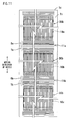
- Fig. 11 is a plan view showing a mask pattern of a third embodiment.
- the third embodiment is applied to a multiple making process in which partitions for a plurality of PDPs are formed on one substrate simultaneously, and then the substrate is divided.
- the example shown in Fig. 11 shows an example in which partitions for three PDPs are formed simultaneously, and each of the three display areas 10a, 10b and 10c in Fig. 11 corresponds to a partition portion of one PDP.
- the partition pattern of the PDP of the third embodiment is also a stripe pattern.
- the partition is formed by the process in the same way as the first embodiment, which includes patterning a sheet-like partition material 2c that covers the entire surface of a glass substrate 1c by using a sandblasting process and a mask 30b that is a unit of a main mask and a sub mask, and then baking the partition material 2c.
- the glass substrate 1c has a size of 1460 mm x 1050 mm for manufacturing a 32-inch PDP.
- the display areas 10a, 10b and 10c are arranged with a space along the vertical direction in Fig. 11, and one mask 30b is arranged for each of them.
- auxiliary masks 6a, 7a, 6b and 7b are formed in the non-display areas 11a and 11b between the neighboring display areas at the same time as formation of the mask 30b.
- the auxiliary masks 6a, 7a, 6b and 7b reduce the jet pressure toward the sub partition that is formed by the mask 30b.
- the middle portion in the moving direction of the glass substrate 1c receives larger jet pressure than the end portions do. It is because that approximately a half of the jet deviates to the outside the glass substrate 1c at the end portions.
- auxiliary masks 6a, 7a, 6b and 7b at portions that receive large jet pressure can prevent the mask 30b from being exfoliated, so that exact partitions as designed can be formed in the display areas 10a, 10b and 10c.
- a stepper type pattern exposure is performed in which one photo mask having a size corresponding to one PDP is used three times. For this reason, auxiliary masks are formed actually also for each of the display areas 10a, 10b and 10c similarly, as shown in Fig. 11.
- the quantity of a projection can be suppressed to 12 ⁇ m or less. Even if variation among manufactured panels is taken into account, it can be suppressed to 16 ⁇ m or less. Thus, operation sound (buzz sound) due to vibration during operation of the panel can be suppressed.
- the method for forming partitions according to the present invention enables formation of partitions having exact pattern and height as designed in a display area without generating projections that may disturb the contact between substrates. Therefore, it is useful for improving yields in manufacturing the plasma display panel that can be lowered due to patterning errors and for providing a plasma display panel that does not generate vibration sound due to insufficient contact between substrates.
Landscapes
- Engineering & Computer Science (AREA)
- Physics & Mathematics (AREA)
- Plasma & Fusion (AREA)
- Manufacturing & Machinery (AREA)
- Gas-Filled Discharge Tubes (AREA)
Abstract
Description
Claims (14)
- A method for forming partitions of a plasma display panel, the partitions dividing a discharge space of a plasma display panel, the method comprising the steps of:providing a sheet-like partition material on a substrate that is a panel material, the partition material covering a display area and outside thereof on a surface of the substrate;providing a mask for patterning on the partition material, the mask covering the display area and the outside thereof, so that a pattern of the portion arranged in the display area of the mask corresponds to the partitions, and a pattern of the portion arranged outside of the display area of the mask is a pattern for dividing a band-like portion along a rim of the display area as a grid;patterning the partition material covered partially with the mask by a sandblasting process; andbaking the partition material after the patterning.
- The method for forming partitions of a plasma display panel according to claim 1, further comprising the steps of:providing the mask so as to cover the display area and both sides thereof in a first direction; andmoving a nozzle for ejecting a cutting material relatively to the partition material in the first direction in a reciprocating manner while patterning the partition material by the sandblasting process.
- The method for forming partitions of a plasma display panel according to claim 2, further comprising the step of forming an auxiliary mask outside the mask in the first direction with a distance from the mask at the same time when forming the mask.
- The method for forming partitions of a plasma display panel according to claim 3, wherein both ends of the auxiliary mask in a second direction that is perpendicular to the first direction protrudes from the mask.
- The method for forming partitions of a plasma display panel according to claim 4, wherein the pattern of the auxiliary mask is a stripe pattern in which a plurality of long bands is arranged in parallel in the second direction.
- The method for forming partitions of a plasma display panel according to claim 4, wherein the pattern of the auxiliary mask is a stripe pattern in which a plurality of long thin bands is arranged in parallel in the second direction and at least both ends of the band that is closest to the mask are not protruded from the mask.
- The method for forming partitions of a plasma display panel according to claim 4, wherein the pattern of the auxiliary mask is a ring pattern that is oblong in the second direction.
- The method for forming partitions of a plasma display panel according to claim 1, wherein a corner portion of the mask has an arcuate shape.
- The method for forming partitions of a plasma display panel according to claim 4, wherein the pattern of the auxiliary mask is a pattern in which a plurality of bands that is shorter than the entire length of the display area in the second direction is arranged in parallel to each other as a plurality of discontinuous lines along the second direction.
- The method for forming partitions of a plasma display panel according to claim 9, wherein discontinuous points are shifted from each other among the plural discontinuous lines in the pattern of the auxiliary mask.
- The method for forming partitions of a plasma display panel according to claim 9, wherein the length of the band in the pattern of the auxiliary mask has a value within the range of 0.05-200 mm.
- The method for forming partitions of a plasma display panel according to claim 9, wherein both the width and the length of the band in the pattern of the auxiliary mask have a value less than 240 µm.
- The method for forming partitions of a plasma display panel according to claim 1, wherein at least the width of the band located at the most outside portion among the bands constituting a grid-like pattern of the portion arranged outside of the display area of the mask has a value within the range of 160-320 µm.
- A method for forming partitions that divide a discharge space in each of plural plasma display panels simultaneously, the method comprising the steps of:providing a sheet-like partition material on a substrate that is a panel material on which display areas corresponding to the plural plasma display panels respectively are arranged linearly, the partition material covering the plural display areas and outside thereof on a surface of the substrate;providing a mask for patterning on the partition material, the mask covering the inside and the outside of the display area for each display area, so that a pattern of the portion arranged in the display area of the mask corresponds to the partitions, and a pattern of the portion arranged outside of the display area of the mask is a pattern for dividing a band-like portion along a rim of the display area as a grid;forming an auxiliary mask at least between neighboring masks with a distance from the mask at the same time when forming the mask;patterning the partition material covered partially with the mask and the auxiliary mask by a sandblasting process; andbaking the partition material after the patterning.
Priority Applications (1)
| Application Number | Priority Date | Filing Date | Title |
|---|---|---|---|
| EP09177921A EP2166555A3 (en) | 2001-04-09 | 2002-04-03 | Plasma Display Panel |
Applications Claiming Priority (3)
| Application Number | Priority Date | Filing Date | Title |
|---|---|---|---|
| JP2001110647 | 2001-04-09 | ||
| JP2001110647 | 2001-04-09 | ||
| PCT/JP2002/003362 WO2002084689A1 (en) | 2001-04-09 | 2002-04-03 | Partition wall forming method for plasma display panels using sandblast |
Publications (2)
| Publication Number | Publication Date |
|---|---|
| EP1388876A1 true EP1388876A1 (en) | 2004-02-11 |
| EP1388876A4 EP1388876A4 (en) | 2007-10-03 |
Family
ID=18962378
Family Applications (2)
| Application Number | Title | Priority Date | Filing Date |
|---|---|---|---|
| EP09177921A Withdrawn EP2166555A3 (en) | 2001-04-09 | 2002-04-03 | Plasma Display Panel |
| EP20020714448 Withdrawn EP1388876A4 (en) | 2001-04-09 | 2002-04-03 | METHOD FOR MANUFACTURING A WALL FOR PLASMA DISPLAY PANELS USING SAND JET |
Family Applications Before (1)
| Application Number | Title | Priority Date | Filing Date |
|---|---|---|---|
| EP09177921A Withdrawn EP2166555A3 (en) | 2001-04-09 | 2002-04-03 | Plasma Display Panel |
Country Status (7)
| Country | Link |
|---|---|
| US (4) | US6855026B2 (en) |
| EP (2) | EP2166555A3 (en) |
| JP (3) | JP4027233B2 (en) |
| KR (3) | KR100887033B1 (en) |
| CN (6) | CN1326179C (en) |
| TW (1) | TWI283883B (en) |
| WO (1) | WO2002084689A1 (en) |
Cited By (5)
| Publication number | Priority date | Publication date | Assignee | Title |
|---|---|---|---|---|
| EP1659606A1 (en) * | 2004-11-23 | 2006-05-24 | LG Electronics, Inc. | Plasma display panel |
| EP1670022A1 (en) * | 2004-12-10 | 2006-06-14 | Samsung SDI Co., Ltd. | Plasma display panel |
| EP1713109A3 (en) * | 2005-04-13 | 2007-12-26 | Samsung SDI Co., Ltd. | Plasma display panel |
| EP2068340A2 (en) | 2007-12-05 | 2009-06-10 | Samsung SDI Co., Ltd. | Plasma display panel and method of forming a plasma display panel |
| WO2024039355A3 (en) * | 2022-08-19 | 2024-04-18 | Vestel Beyaz Esya Sanayi Ve Ticaret Anonim Sirketi | A control panel for domestic appliances |
Families Citing this family (17)
| Publication number | Priority date | Publication date | Assignee | Title |
|---|---|---|---|---|
| CN1326179C (en) * | 2001-04-09 | 2007-07-11 | 富士通株式会社 | Method for forming partition wall of plasma display panel by sandblasting |
| JP4136799B2 (en) * | 2002-07-24 | 2008-08-20 | 富士フイルム株式会社 | Method for forming EL display element |
| KR100522686B1 (en) | 2002-11-05 | 2005-10-19 | 삼성에스디아이 주식회사 | Plasma display panel |
| KR100573161B1 (en) | 2004-08-30 | 2006-04-24 | 삼성에스디아이 주식회사 | Plasma display panel |
| KR100590040B1 (en) * | 2004-09-23 | 2006-06-14 | 삼성에스디아이 주식회사 | Manufacturing Method of Plasma Display Panel |
| US7675234B2 (en) * | 2005-08-31 | 2010-03-09 | Chunghwa Picture Tubes, Ltd. | Plasma display panel having honeycomb supporting structures |
| KR100749464B1 (en) | 2005-09-29 | 2007-08-14 | 삼성에스디아이 주식회사 | Plasma display panel |
| JP4887734B2 (en) * | 2005-10-31 | 2012-02-29 | パナソニック株式会社 | Plasma display panel |
| JPWO2007138700A1 (en) * | 2006-05-31 | 2009-10-01 | 日立プラズマディスプレイ株式会社 | Plasma display panel and manufacturing method thereof |
| JP2008018518A (en) * | 2006-07-14 | 2008-01-31 | Fujitsu Hitachi Plasma Display Ltd | Method and device for forming barrier rib of plasma display panel |
| TW200830931A (en) * | 2007-01-08 | 2008-07-16 | Tatung Co Ltd | Method for manufacturing the spacer for field emission device and base material utilized for the spacer |
| US8597288B2 (en) * | 2008-10-01 | 2013-12-03 | St. Jude Medical, Artial Fibrillation Division, Inc. | Vacuum-stabilized ablation system |
| KR20100043498A (en) * | 2008-10-20 | 2010-04-29 | 삼성에스디아이 주식회사 | Plsama display panel and the fabrication method thereof |
| TWI438160B (en) * | 2010-07-14 | 2014-05-21 | Hon Hai Prec Ind Co Ltd | Glass processing equipment |
| TW201208816A (en) * | 2010-08-27 | 2012-03-01 | Hon Hai Prec Ind Co Ltd | Fixing device and glass processing equipment using same |
| TWI438161B (en) * | 2010-10-12 | 2014-05-21 | Hon Hai Prec Ind Co Ltd | Glass processing equipment |
| CN108642440B (en) | 2018-05-14 | 2019-09-17 | 昆山国显光电有限公司 | Mask plate and mask assembly |
Family Cites Families (19)
| Publication number | Priority date | Publication date | Assignee | Title |
|---|---|---|---|---|
| JPH0745193B2 (en) | 1987-06-26 | 1995-05-17 | 株式会社フジクラ | CV cable connection method |
| JP3279753B2 (en) * | 1993-07-30 | 2002-04-30 | 大日本印刷株式会社 | Method for forming barrier of plasma display panel |
| TW320732B (en) * | 1995-04-20 | 1997-11-21 | Matsushita Electron Co Ltd | |
| US5684362A (en) * | 1995-07-25 | 1997-11-04 | Sony Corporation | Plasma addressed electro-optical device having a plasma discharge chamber |
| JPH09115452A (en) * | 1995-10-13 | 1997-05-02 | Sumitomo Kinzoku Electro Device:Kk | Barrier structure of plasma display panel |
| JP3624992B2 (en) * | 1996-04-22 | 2005-03-02 | 富士通株式会社 | Method for forming partition wall of display panel |
| JPH10319875A (en) * | 1997-05-20 | 1998-12-04 | Sony Corp | Manufacturing method of plasma address display device |
| JPH117897A (en) | 1997-06-13 | 1999-01-12 | Hitachi Ltd | Gas discharge type display panel and display device using the same |
| JP3427699B2 (en) * | 1997-10-17 | 2003-07-22 | 富士通株式会社 | Method of forming partition wall of plasma display panel |
| JPH11191377A (en) * | 1997-12-26 | 1999-07-13 | Hitachi Chem Co Ltd | Barrier of plasma display panel and its manufacture |
| JP3705914B2 (en) | 1998-01-27 | 2005-10-12 | 三菱電機株式会社 | Surface discharge type plasma display panel and manufacturing method thereof |
| JP3599316B2 (en) | 1999-04-26 | 2004-12-08 | パイオニア株式会社 | Plasma display panel |
| US6465956B1 (en) | 1998-12-28 | 2002-10-15 | Pioneer Corporation | Plasma display panel |
| JP3569458B2 (en) * | 1999-03-26 | 2004-09-22 | パイオニア株式会社 | Plasma display panel |
| JP2001052616A (en) | 1999-08-12 | 2001-02-23 | Toray Ind Inc | Plasma display member and plasma display using the same |
| JP2001236890A (en) * | 2000-02-25 | 2001-08-31 | Mitsubishi Electric Corp | Gas discharge display panel and method of manufacturing the same |
| US6428945B1 (en) * | 2001-02-13 | 2002-08-06 | Au Optronics Corp. | Method of forming barrier ribs used in a plasma display panel |
| CN1326179C (en) * | 2001-04-09 | 2007-07-11 | 富士通株式会社 | Method for forming partition wall of plasma display panel by sandblasting |
| CN1129947C (en) * | 2001-06-12 | 2003-12-03 | 友达光电股份有限公司 | Manufacturing method of barrier rib of plasma display and structure of back plate of display |
-
2002
- 2002-04-03 CN CNB028079914A patent/CN1326179C/en not_active Expired - Fee Related
- 2002-04-03 EP EP09177921A patent/EP2166555A3/en not_active Withdrawn
- 2002-04-03 CN CNB2007101049439A patent/CN100570794C/en not_active Expired - Fee Related
- 2002-04-03 CN CN200710104944A patent/CN100590769C/en not_active Expired - Fee Related
- 2002-04-03 KR KR1020087005766A patent/KR100887033B1/en not_active Expired - Fee Related
- 2002-04-03 EP EP20020714448 patent/EP1388876A4/en not_active Withdrawn
- 2002-04-03 KR KR1020087014719A patent/KR100889161B1/en not_active Expired - Fee Related
- 2002-04-03 CN CN200710104941XA patent/CN101075518B/en not_active Expired - Fee Related
- 2002-04-03 JP JP2002581544A patent/JP4027233B2/en not_active Expired - Fee Related
- 2002-04-03 CN CN200710104942A patent/CN100580851C/en not_active Expired - Fee Related
- 2002-04-03 KR KR1020037013146A patent/KR100887040B1/en not_active Expired - Fee Related
- 2002-04-03 CN CN2007101049405A patent/CN101075517B/en not_active Expired - Fee Related
- 2002-04-03 WO PCT/JP2002/003362 patent/WO2002084689A1/en not_active Ceased
- 2002-04-12 TW TW091107473A patent/TWI283883B/en not_active IP Right Cessation
-
2003
- 2003-10-08 US US10/680,136 patent/US6855026B2/en not_active Ceased
-
2007
- 2007-02-14 US US11/705,796 patent/USRE41312E1/en not_active Expired - Lifetime
- 2007-07-23 JP JP2007190853A patent/JP4480743B2/en not_active Expired - Fee Related
- 2007-07-23 JP JP2007190849A patent/JP4480742B2/en not_active Expired - Fee Related
-
2008
- 2008-12-04 US US12/328,197 patent/USRE42405E1/en not_active Expired - Lifetime
-
2011
- 2011-05-27 US US13/117,892 patent/USRE44445E1/en not_active Expired - Fee Related
Cited By (8)
| Publication number | Priority date | Publication date | Assignee | Title |
|---|---|---|---|---|
| EP1659606A1 (en) * | 2004-11-23 | 2006-05-24 | LG Electronics, Inc. | Plasma display panel |
| US7569990B2 (en) | 2004-11-23 | 2009-08-04 | Lg Electronics Inc. | Plasma display panel having main and quxiliary barrier ribs |
| EP1670022A1 (en) * | 2004-12-10 | 2006-06-14 | Samsung SDI Co., Ltd. | Plasma display panel |
| US7501759B2 (en) | 2004-12-10 | 2009-03-10 | Samsung Sdi Co., Ltd. | Plasma display panel |
| EP1713109A3 (en) * | 2005-04-13 | 2007-12-26 | Samsung SDI Co., Ltd. | Plasma display panel |
| US7649314B2 (en) | 2005-04-13 | 2010-01-19 | Samsung Sdi Co., Ltd. | Plasma display panel |
| EP2068340A2 (en) | 2007-12-05 | 2009-06-10 | Samsung SDI Co., Ltd. | Plasma display panel and method of forming a plasma display panel |
| WO2024039355A3 (en) * | 2022-08-19 | 2024-04-18 | Vestel Beyaz Esya Sanayi Ve Ticaret Anonim Sirketi | A control panel for domestic appliances |
Also Published As
Similar Documents
| Publication | Publication Date | Title |
|---|---|---|
| USRE41312E1 (en) | Method for forming partitions of plasma display panel by using sandblasting process | |
| US8025543B2 (en) | Method of manufacturing a partition wall structure on a plasma display panel | |
| US20050242696A1 (en) | Plasma display panel and method of fabricating the same | |
| JP3624992B2 (en) | Method for forming partition wall of display panel | |
| JPH10188791A (en) | Display panel partition wall forming method | |
| US7755284B2 (en) | Plasma display panel | |
| EP1672665B1 (en) | Method of applying phosphor paste of PDP | |
| JP3620939B2 (en) | Method for forming partition wall of display panel | |
| JP3161580B2 (en) | Pattern formation method | |
| JP2005294060A (en) | Substrate for plasma display panel |
Legal Events
| Date | Code | Title | Description |
|---|---|---|---|
| PUAI | Public reference made under article 153(3) epc to a published international application that has entered the european phase |
Free format text: ORIGINAL CODE: 0009012 |
|
| 17P | Request for examination filed |
Effective date: 20031006 |
|
| AK | Designated contracting states |
Kind code of ref document: A1 Designated state(s): AT BE CH CY DE DK ES FI FR GB GR IE IT LI LU MC NL PT SE TR |
|
| AX | Request for extension of the european patent |
Extension state: AL LT LV MK RO SI |
|
| RAP1 | Party data changed (applicant data changed or rights of an application transferred) |
Owner name: FUJITSU HITACHI PLASMA DISPLAY LIMITED Owner name: HITACHI, LTD. |
|
| RAP1 | Party data changed (applicant data changed or rights of an application transferred) |
Owner name: FUJITSU HITACHI PLASMA DISPLAY LIMITED Owner name: HITACHI PLASMA PATENT LICENSING CO., LTD. |
|
| RIC1 | Information provided on ipc code assigned before grant |
Ipc: H01J 9/24 20060101AFI20070817BHEP |
|
| A4 | Supplementary search report drawn up and despatched |
Effective date: 20070903 |
|
| RAP1 | Party data changed (applicant data changed or rights of an application transferred) |
Owner name: HITACHI PLASMA DISPLAY LIMITED Owner name: HITACHI PLASMA PATENT LICENSING CO., LTD. |
|
| 17Q | First examination report despatched |
Effective date: 20100503 |
|
| RAP1 | Party data changed (applicant data changed or rights of an application transferred) |
Owner name: HITACHI, LTD. Owner name: HITACHI PLASMA PATENT LICENSING CO., LTD. |
|
| RAP1 | Party data changed (applicant data changed or rights of an application transferred) |
Owner name: HITACHI CONSUMER ELECTRONICS CO., LTD. Owner name: HITACHI, LTD. |
|
| RAP1 | Party data changed (applicant data changed or rights of an application transferred) |
Owner name: HITACHI CONSUMER ELECTRONICS CO., LTD. |
|
| RIC1 | Information provided on ipc code assigned before grant |
Ipc: H01J 11/36 20120101ALI20150309BHEP Ipc: H01J 11/12 20120101ALI20150309BHEP Ipc: H01J 9/24 20060101AFI20150309BHEP |
|
| GRAP | Despatch of communication of intention to grant a patent |
Free format text: ORIGINAL CODE: EPIDOSNIGR1 |
|
| RAP1 | Party data changed (applicant data changed or rights of an application transferred) |
Owner name: HITACHI MAXELL, LTD. |
|
| RBV | Designated contracting states (corrected) |
Designated state(s): DE FR GB |
|
| INTG | Intention to grant announced |
Effective date: 20150429 |
|
| RIN1 | Information on inventor provided before grant (corrected) |
Inventor name: KANAE, TATSUTOSHI Inventor name: KAWANAMI, YOSHIMI Inventor name: TOYODA, OSAMU Inventor name: ISHIZUKA, KAZUNORI Inventor name: KUNII, YASUHIKO Inventor name: NANTO, TOSHIYUKI Inventor name: KOSAKA, TADAYOSHI Inventor name: IWASAKI, KAZUHIDE Inventor name: SHIRAKAWA, YOSHIMI Inventor name: FUJINAGA, AKIHIRO Inventor name: SHIBATA, MASAYUKI |
|
| STAA | Information on the status of an ep patent application or granted ep patent |
Free format text: STATUS: THE APPLICATION IS DEEMED TO BE WITHDRAWN |
|
| 18D | Application deemed to be withdrawn |
Effective date: 20150910 |