EP1387344A2 - Method and apparatus for driving plasma display panel - Google Patents
Method and apparatus for driving plasma display panel Download PDFInfo
- Publication number
- EP1387344A2 EP1387344A2 EP03254796A EP03254796A EP1387344A2 EP 1387344 A2 EP1387344 A2 EP 1387344A2 EP 03254796 A EP03254796 A EP 03254796A EP 03254796 A EP03254796 A EP 03254796A EP 1387344 A2 EP1387344 A2 EP 1387344A2
- Authority
- EP
- European Patent Office
- Prior art keywords
- control signal
- temperature
- ramp waveform
- width
- driving apparatus
- Prior art date
- Legal status (The legal status is an assumption and is not a legal conclusion. Google has not performed a legal analysis and makes no representation as to the accuracy of the status listed.)
- Withdrawn
Links
Images


Classifications
-
- G—PHYSICS
- G09—EDUCATION; CRYPTOGRAPHY; DISPLAY; ADVERTISING; SEALS
- G09G—ARRANGEMENTS OR CIRCUITS FOR CONTROL OF INDICATING DEVICES USING STATIC MEANS TO PRESENT VARIABLE INFORMATION
- G09G3/00—Control arrangements or circuits, of interest only in connection with visual indicators other than cathode-ray tubes
- G09G3/20—Control arrangements or circuits, of interest only in connection with visual indicators other than cathode-ray tubes for presentation of an assembly of a number of characters, e.g. a page, by composing the assembly by combination of individual elements arranged in a matrix no fixed position being assigned to or needed to be assigned to the individual characters or partial characters
- G09G3/22—Control arrangements or circuits, of interest only in connection with visual indicators other than cathode-ray tubes for presentation of an assembly of a number of characters, e.g. a page, by composing the assembly by combination of individual elements arranged in a matrix no fixed position being assigned to or needed to be assigned to the individual characters or partial characters using controlled light sources
- G09G3/28—Control arrangements or circuits, of interest only in connection with visual indicators other than cathode-ray tubes for presentation of an assembly of a number of characters, e.g. a page, by composing the assembly by combination of individual elements arranged in a matrix no fixed position being assigned to or needed to be assigned to the individual characters or partial characters using controlled light sources using luminous gas-discharge panels, e.g. plasma panels
- G09G3/288—Control arrangements or circuits, of interest only in connection with visual indicators other than cathode-ray tubes for presentation of an assembly of a number of characters, e.g. a page, by composing the assembly by combination of individual elements arranged in a matrix no fixed position being assigned to or needed to be assigned to the individual characters or partial characters using controlled light sources using luminous gas-discharge panels, e.g. plasma panels using AC panels
- G09G3/291—Control arrangements or circuits, of interest only in connection with visual indicators other than cathode-ray tubes for presentation of an assembly of a number of characters, e.g. a page, by composing the assembly by combination of individual elements arranged in a matrix no fixed position being assigned to or needed to be assigned to the individual characters or partial characters using controlled light sources using luminous gas-discharge panels, e.g. plasma panels using AC panels controlling the gas discharge to control a cell condition, e.g. by means of specific pulse shapes
- G09G3/292—Control arrangements or circuits, of interest only in connection with visual indicators other than cathode-ray tubes for presentation of an assembly of a number of characters, e.g. a page, by composing the assembly by combination of individual elements arranged in a matrix no fixed position being assigned to or needed to be assigned to the individual characters or partial characters using controlled light sources using luminous gas-discharge panels, e.g. plasma panels using AC panels controlling the gas discharge to control a cell condition, e.g. by means of specific pulse shapes for reset discharge, priming discharge or erase discharge occurring in a phase other than addressing
- G09G3/2927—Details of initialising
-
- G—PHYSICS
- G09—EDUCATION; CRYPTOGRAPHY; DISPLAY; ADVERTISING; SEALS
- G09G—ARRANGEMENTS OR CIRCUITS FOR CONTROL OF INDICATING DEVICES USING STATIC MEANS TO PRESENT VARIABLE INFORMATION
- G09G2310/00—Command of the display device
- G09G2310/06—Details of flat display driving waveforms
-
- G—PHYSICS
- G09—EDUCATION; CRYPTOGRAPHY; DISPLAY; ADVERTISING; SEALS
- G09G—ARRANGEMENTS OR CIRCUITS FOR CONTROL OF INDICATING DEVICES USING STATIC MEANS TO PRESENT VARIABLE INFORMATION
- G09G2310/00—Command of the display device
- G09G2310/06—Details of flat display driving waveforms
- G09G2310/066—Waveforms comprising a gently increasing or decreasing portion, e.g. ramp
Abstract

Description
- This invention relates to a plasma display panel, and more particularly to a method and apparatus of driving a plasma display panel to improve stability of operation at both low and high temperatures.
- Generally, a plasma display panel (PDP) uses ultraviolet rays generated upon discharge of an inactive mixture gas such as He+Xe, Ne+Xe or He+Ne+Xe to excite a phosphorus material which then re-emits photons, to thereby display a picture. Such a PDP is easy to manufacture in thin-film and large-dimension formats. Moreover, such PDPs provide increasingly better picture quality owing to recent technical developments.
- Referring to Fig. 1, a discharge cell of a conventional three-electrode, AC surface-discharge PDP includes a sustain electrode pair having a scan electrode 30Y, a common sustain electrode 30Z provided on an
upper substrate 10, and anaddress electrode 20X provided on alower substrate 18 in such a manner to perpendicularly cross the sustain electrode pair. Each of the scan electrode 30Y and the common sustain electrode 30Z has a structure disposed withtransparent electrodes metal bus electrodes upper substrate 10 provided, in parallel, with the scan electrode 30Y and the common sustain electrode 30Z, an upperdielectric layer 14 and an MgOprotective film 16 are disposed. A lowerdielectric layer 22 andbarrier ribs 24 are formed on thelower substrate 18 provided with theaddress electrode 20X, and aphosphorous material layer 26 is coated onto the surfaces of the lowerdielectric layer 22 and thebarrier ribs 24. An inactive mixture gas such as He+Xe, Ne+Xe or He+Ne+Xe is injected into a discharge space among theupper substrate 10, thelower substrate 18 and thebarrier ribs 24. - Such a PDP makes a time-divisional driving of one frame, which is divided into various sub-fields having a different emission frequency, so as to realize gray levels of a picture. Each sub-field is again divided into an initialization period for initializing the entire field, an address period for selecting a scan line and selecting the cell from the selected scan line and a sustain period for expressing gray levels depending on the discharge frequency. The initialization period is divided into a set-up interval supplied with a rising ramp waveform and a set-down interval supplied with a falling ramp waveform.
- For instance, when it is intended to display a picture of 256 gray levels, a frame interval equal to 1/60 second (i.e. 16.67 msec) is divided into 8 sub-fields SF1 to SF8 as shown in Fig. 2. Each of the 8 sub-field SF1 to SF8 is divided into an initialization period, an address period and a sustain period as mentioned above. Herein, the initialization period and the address period of each sub-field are equal for each sub-field, whereas the sustain period and the number of sustain pulses assigned thereto are increased at a ratio of 2n (wherein n = 0, 1, 2, 3, 4, 5, 6 and 7) at each sub-field.
- Fig. 3 shows a driving waveform of the PDP applied to two sub-fields. Herein, Y represents the scan electrode; Z does the common sustain electrode; and X does the address electrode.
- Referring to Fig. 3, the PDP is divided into an initialization period for initializing the full field, an address period for selecting a cell, and a sustain period for sustaining a discharge of the selected cell for its driving.
- In the initialization period, a rising ramp waveform Ramp-up is simultaneously applied all the scan electrodes Y in a set-up interval SU. A discharge is generated within the cells at the full field with the aid of the rising ramp waveform Ramp-up. By this set-up discharge, positive wall charges are accumulated onto the address electrode X and the sustain electrode Z while negative wall charges are accumulated onto the scan electrode Y. In a set-down interval SD, a falling ramp waveform Ramp-down falling from a positive voltage lower than a peak voltage of the rising ramp waveform Ramp-up is simultaneously applied to the scan electrodes Y after the rising ramp waveform Ramp-up was applied. The falling ramp waveform Ramp-down causes a weak erasure discharge within the cells to erase a portion of excessively formed wall charges. Wall charges enough to generate a stable address discharge are uniformly left within the cells with the aid of the set-down discharge.
- In the address period, a negative scanning pulse scan is sequentially applied to the scan electrodes Y and, at the same time, a positive data pulse data is applied to the address electrodes X in synchronization with the scanning pulse scan. A voltage difference between the scanning pulse scan and the data pulse data is added to a wall voltage generated in the initialization period to thereby generate an address discharge within the cells supplied with the data pulse data. Wall charges enough to cause a discharge when a sustain voltage is applied are formed within the cells selected by the address discharge.
- Meanwhile, a positive direct current voltage Zdc is applied to the common sustain electrodes Z during the set-down interval and the address period. The direct current voltage Zdc causes a set-down discharge between the common sustain electrode Z, and allows an address discharge generated between the scan electrode Y and the address electrode X in the address period to be transited into a surface discharge between the scan electrode Y and the common sustain electrode Z.
- In the sustain period, a sustaining pulse sus is alternately applied to the scan electrodes Y and the common sustain electrodes Z. Then, a wall voltage within the cell selected by the address discharge is added to the sustain pulse sus to thereby generate a sustain discharge, that is, a display discharge between the scan electrode Y and the common sustain electrode Z whenever the sustain pulse sus is applied.
- Finally, after the sustain discharge was finished, a ramp waveform erase having a small pulse width and a low voltage level is applied to the common sustain electrode Z to thereby erase wall charges left within the cells of the entire field.
- However, such a conventional PDP has a problem in that a brightness point mis-discharge or no discharge occurs at a high temperature (i.e., more than 40°C) and a low temperature (i.e., approximately 20°C to -50°C) upon driving. More specifically, when the PDP is driven at a high temperature atmosphere more than about 40°C with being divided into a first half and a second half as shown in Fig. 4, that is, by a double scan strategy, there is raised a problem in that no address discharge occurs at the
middle portion 41 of the screen having a late scanning sequence. Likewise, when the PDP is scanned at a high temperature atmosphere more than about 40°C sequentially from the first line until the last line as shown in Fig. 5, that is, by a single scan strategy, there is raised a problem in that no address discharge occurs at thelower portion 51 of the screen having a late scanning sequence. - As a result of many experiments and analyses as to the experiments, a major factor causing a misfire at a high temperature atmosphere is because a loss amount of wall charges generated in the initialization period is more increased as a scanning sequence is later. Such a factor will be described on a basis of a discharge characteristic change within the cell below. Firstly, as an internal/external temperature of the cell rises, wall charges are lost due to a leakage current generated from deterioration in an insulation property of a dielectric material and a protective layer within the cell. Secondary, as a motion of space charges within the cell is more activated, a re-combination of the space charges with atoms having lost electrons is easily generated. Thus, wall charges and space charges contributed to the discharge are lost with the lapse of time.
- Furthermore, when the PDP is driven at a low temperature atmosphere less than 20°C, a motion of particles becomes dull to generate a brightness point misfire. More specifically, if a motion of particles becomes dull at a low temperature, then an erasure discharge caused by an erasing ramp waveform erase is not normally generated. Wall charges formed at the scan electrode Y and the common sustain electrode Z are not erased from the cells having such an abnormal erasure discharge.
- Thereafter, a positive rising ramp waveform Ramp-up is applied to the scan electrode Y in the set-up interval. At this time, since negative wall charges has been formed at the scan electrode Y, that is, since a voltage applied to the scan electrode Y and wall charges having been formed at the scan electrode Y has an opposite polarity with respect to each other, a normal discharge is not generated in the set-up interval. Further, in the set-down interval following the set-up interval, a normal discharge is not generated. If a normal discharge does not occur in the initialization period, then wall charges formed excessively in the erasure period make an affect to the address period and the sustain period. In other words, wall charges formed excessively at the discharge cells cause an undesired strong discharge taking a brightness point shape in the sustain period.
- Accordingly, it would be desirable to provide a method and apparatus of driving a plasma display panel that improves the stability of operation at both low and high temperatures.
- In order to achieve these and other objects of the invention, a driving apparatus for a plasma display panel according to one aspect of the present invention includes a scan driver for supplying a rising ramp waveform in a set-up interval and a falling ramp waveform in a set-down interval; a temperature sensor for sensing a driving temperature of the panel to generate a bit control signal; and a set-down control signal generator for generating a control signal such that an application time of the falling ramp waveform can be controlled in correspondence with said bit control signal and for applying the control signal to the scan driver.
- Preferably, said temperature sensor generates different bit control signals at a high temperature and at a temperature less than the high temperature.
- Preferably, said set-down control signal generator sets a width of said control signal such that a width of the control signal applied at said high temperature is narrower than that of the control signal applied at a temperature less than the high temperature in correspondence with said bit control signal.
- Said scan driver may supply said falling ramp waveform during a time corresponding to said width of the control signal.
- Said temperature sensor may divide the high temperature into a plurality of temperature levels, and generates said different bit control signals for each temperature level.
- Said set-down control signal generator may generate a control signal having a narrower width as the temperature level goes higher, and said scan driver supplies said falling ramp waveform during a time corresponding to said width of the control signal.
- A driving apparatus for a plasma display panel according to another aspect of the present invention includes a scan driver for supplying a rising ramp waveform in a set-up interval and a falling ramp waveform in a set-down interval; a temperature sensor for sensing a driving temperature of the panel to generate a bit control signal; and a set-up control signal generator for generating a control signal such that an application time of the rising ramp waveform can be controlled in correspondence with said bit control signal and for applying the control signal to the scan driver.
- Preferably, said temperature sensor generates different bit control signals at a low temperature and at a temperature more than the low temperature.
- Preferably, said set-up control signal generator sets a width of said control signal such that a width of the control signal applied at said low temperature is narrower than that of the control signal applied at said temperature more than the low temperature in correspondence with said bit control signal.
- Said scan driver may supply said rising ramp waveform during a time corresponding to said width of the control signal.
- Said temperature sensor may divide the low temperature into a plurality of temperature levels, and generates said different bit control signals for each temperature level.
- Said set-up control signal generator may generate a control signal having a larger width as the temperature level goes lower, and said scan driver supplies said rising ramp waveform during a time corresponding to said width of the control signal.
- A driving apparatus for a plasma display panel according to still another aspect of the present invention includes a scan driver for supplying a rising ramp waveform in a set-up interval and a falling ramp waveform in a set-down interval; a first temperature sensor for sensing a driving temperature of the panel to generate a first bit control signal; a second temperature sensor for sensing a driving temperature of the panel to generate a second bit control signal; a set-up control signal generator for generating a first control signal such that an application time of the rising ramp waveform can be controlled in correspondence with said first bit control signal and for applying the first control signal to the scan driver; and a set-down control signal generator for generating a second control signal such that an application time of the falling ramp waveform can be controlled in correspondence with said second bit control signal and for applying the second control signal to the scan driver.
- Preferably, said first temperature sensor generates first different bit control signals at a low temperature and at a temperature more than the low temperature, and said second temperature generates second different bit control signals at a high temperature and a temperature less than the high temperature.
- Preferably, said set-up control signal generator sets a width of said first control signal such that a width of the first control signal applied at said low temperature is larger than that of the first control signal applied at said temperature more than the low temperature in correspondence with said first bit control signal, and said set-down control signal generator sets a width of said second control signal such that a width of the second control signal applied at said high temperature is narrower than that of the second control signal applied at said temperature less than the high temperature in correspondence with said second bit control signal.
- Said scan driver may supply said rising ramp waveform during a time corresponding to said width of the first control signal, and supplies said falling ramp waveform during a time corresponding to said width of the second control signal.
- Said first temperature sensor may divide the low temperature into a plurality of temperature levels and generates said first different bit control signals for each low temperature level, and said second temperature sensor divides the high temperature into a plurality of temperature levels and generates said second different bit control signals for each high temperature level.
- Said set-up control signal generator may generate a first control signal having a larger width as the low temperature level goes lower, and said scan driver supplies said rising ramp waveform corresponding to said width of the first control signal.
- Said set-down control signal generator may generate a second control signal having a narrower width as the high temperature level goes higher, and said scan driver supplies said falling ramp waveform corresponding to said width of the second control signal.
- A method of driving a plasma display panel according to still another aspect of the present invention includes the steps of applying a rising ramp waveform to a scan electrode in a set-up interval; applying a falling ramp waveform to the scan electrode in a set-down interval following said set-up interval; and differently setting an application time of said falling ramp waveform applied to the scan electrode at a high temperature and at a temperature less than the high temperature.
- Preferably, said application time of the falling ramp waveform at said high temperature is set to be shorter than that of the falling ramp waveform at said temperature less than the high temperature.
- Preferably, said high temperature is divided into a plurality of temperature levels, and said application time of the falling ramp waveform is more shortly set as said temperature level goes higher.
- A method of driving a plasma display panel according to still another aspect of the present invention includes the steps of applying a rising ramp waveform to a scan electrode in a set-up interval; applying a falling ramp waveform to the scan electrode in a set-down interval following said set-up interval; and differently setting an application time of said rising ramp waveform applied to the scan electrode at a low temperature and at a temperature more than the low temperature.
- Preferably, said application time of the rising ramp waveform at said low temperature is set to be longer than that of the rising ramp waveform at said temperature more than the low temperature.
- Preferably, said low temperature is divided into a plurality of temperature levels, and said application time of the rising ramp waveform is longer set as said temperature level goes lower.
- A slope of the rising ramp waveform applied at said low temperature may be equal to that of the rising ramp waveform applied at said temperature more than the low temperature.
- These and other objects of the invention will be apparent from the following detailed description of the embodiments of the present invention with reference to the accompanying drawings, in which:
- Fig. 1 is a perspective view showing a discharge cell structure of a conventional three-electrode, AC surface-discharge plasma display panel;
- Fig. 2 illustrates one frame in the conventional plasma display panel;
- Fig. 3 is a waveform diagram showing a method of driving the conventional plasma display panel;
- Fig. 4 and Fig. 5 depict an area having a misfire at a high temperature atmosphere in the conventional plasma display panel;
- Fig. 6 depicts wall charges formed at the electrodes when a normal erasure discharge is not generated;
- Fig. 7 is a block diagram showing a configuration of a driving apparatus for a plasma display panel according to a first embodiment of the present invention;
- Fig. 8 is a waveform diagram of a control signal generated from the set-down control signal generator shown in Fig. 7;
- Fig. 9A to Fig. 9C illustrate falling ramp waveforms applied in correspondence with the control signal shown in Fig. 8;
- Fig. 10 is a block diagram showing a configuration of a driving apparatus for a plasma display panel according to a second embodiment of the present invention;
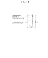
- Fig. 11 is a waveform diagram of a control signal generated from the set-up control signal generator shown in Fig. 10;
- Fig. 12 illustrates a rising ramp waveform applied in correspondence with the control signal shown in Fig. 11; and
- Fig. 13 is a block diagram showing a configuration of a driving apparatus for a plasma display panel according to a third embodiment of the present invention.
-
- Fig. 7 shows a driving apparatus for a plasma display panel (PDP) according to a first embodiment of the present invention.
- Referring to Fig. 7, the driving apparatus includes a
data driver 62 for applying a data pulse to address electrodes X1 to Xm, ascan driver 64 for applying an initialization pulse, a scanning pulse and a sustaining pulse to scan electrodes Y1 to Ym, a sustaindriver 66 for applying a positive direct current (DC) voltage and a sustaining pulse to a common sustain electrode Z, atiming controller 60 for controlling eachdriver temperature sensor 74 for sensing a driving temperature of apanel 61, and a set-downcontrol signal generator 72 for applying a set-down control signal to thescan driver 64. - The
data driver 62 is subject to a reverse gamma correction and an error diffusion, etc. by a reverse gamma correcting circuit and an error diffusing circuit, etc. (not shown), and thereafter latches data mapped onto each sub-field by a sub-field mapping circuit (not shown) under control of thetiming controller 60 and applies the latched data to the address electrodes X1 to Xm. - The
scan driver 64 supplies a rising ramp waveform and a falling ramp waveform to the scan electrodes Y1 to Ym in the initialization period and then sequentially applies a scanning pulse for selecting a scan line to the scan electrodes Yl to Ym in the address period. Further, thescan driver 64 simultaneously applies a sustaining pulse for causing a sustaining discharge for the cell selected in the address period to the scan electrodes Y1 to Ym. Such ascan driver 64 determines an application time of the falling ramp waveform applied in the set-down interval under control of the set-downcontrol signal generator 72. - The sustain
driver 66 supplies a DC voltage in the set-down interval and the address period, and supplies a sustaining pulse in the sustain period. - The
timing controller 60 receives vertical and horizontal synchronizing signals to generate timing control signals required for eachdriver driver - The
temperature sensor 74 applies a desired bit control signal to the set-downcontrol signal generator 72 with sensing a driving temperature of thepanel 61. Thetemperature sensor 74 generates different bit control signals when thepanel 61 is driven at a high temperature (i.e., more than about 40°C) and when thepanel 61 is driven at less than said high temperature and applies them to the set-downcontrol signal generator 72. - Furthermore, the
temperature sensor 74 divides a temperature more than said high temperature into a plurality of levels, and generates a bit control signal corresponding to the temperature level to apply it to the set-downcontrol signal generator 72. For instance, thetemperature sensor 74 may generate a 4-bit control signal corresponding to a driving temperature of thepanel 61 to apply it to the set-downcontrol signal generator 72. - The set-down
control signal generator 72 applies a set-down control signal having a different width in correspondence with the bit control signal inputted from thetemperature sensor 74 to thescan driver 64. - In operation, the
temperature sensor 74 applies a desired bit control signal (e.g., a control signal "0000") to the set-downcontrol signal generator 72 when thepanel 61 is operated at a temperature less than said high temperature. The set-downcontrol signal generator 72 having received the control signal "0000" from thetemperature sensor 74 applies a control signal having a width T1 as shown in Fig. 8 to thescan driver 64. At this time, the width T1 of the control signal applied from the set-downcontrol signal generator 72 is set to be equal to that of the conventional set-down control signal. - The
scan driver 64 receiving a control signal having a width T1 from the set-downcontrol signal generator 72 supplies a falling ramp waveform Ramp-down during the T1 interval in the set-down interval. - This procedure will be described in detail. First, the
scan driver 64 applies a rising ramp waveform Ramp-up to all the scan electrodes as shown in Fig. 9A in the set-up interval of the initialization period. This rising ramp waveform Ramp-up causes a set-up discharge within the cells of the full field, and the set-up discharge allows positive wall charges to be accumulated onto the address electrode X and the common sustain electrode Z and allows negative wall charges to be accumulated onto the scan electrode Y. - In the set-down interval, after the rising ramp waveform Ramp-up was supplied, a falling ramp waveform Ramp-down falling from a positive voltage lower than a peak voltage of the rising ramp waveform Ramp-up is simultaneously applied to the scan electrodes Y during the T1 interval. At this time, the falling ramp waveform Ramp-down falls into a voltage V1. Such a falling ramp waveform Ramp-down causes a weak erasure discharge within the cells to erase a portion of excessive wall charges. Meanwhile, the voltage V1 obtained by a falling of the falling ramp waveform Ramp-down has a voltage difference Vd1 from a voltage level of the scanning pulse scan applied in the address period.
- The
temperature sensor 74 applies a control signal "0001" to the set-downcontrol signal generator 72 when thepanel 61 is operated at a first high temperature (e.g., 42°C) of the plurality of temperature levels. The set-downcontrol signal generator 72 having received the control signal "0001" from thetemperature sensor 74 applies a control signal having a width T2 narrower than the width T1 as shown in Fig. 8 to thescan driver 64. - The
scan driver 64 having received a control signal having the width T2 from the set-downcontrol signal generator 72 applies the falling ramp waveform Ramp-down during the T2 interval in the set-down interval. - This procedure will be described in detail. First, the
scan driver 64 applies a rising ramp waveform Ramp-up to all the scan electrodes as shown in Fig. 9B in the set-up interval of the initialization period. This rising ramp waveform causes a set-up discharge within the cells of the full field, and the set-up discharges allows positive wall charges to be accumulated onto the address electrode X and the common sustain electrode Z and allows negative wall charges to be accumulated onto the scan electrode Y. - In the set-down interval, after the rising ramp waveform Ramp-up was supplied, a falling ramp waveform Ramp-down falling from a positive voltage lower than a peak voltage of the rising ramp waveform Ramp-up is simultaneously applied to the scan electrodes Y during the T2 interval. At this time, the falling ramp waveform Ramp-down falls into a voltage V2 higher than the voltage V1. Such a falling ramp waveform Ramp-down causes a weak erasure discharge within the cells to erase a portion of excessive wall charges.
- At this time, since the falling ramp waveform Ramp-down is supplied only during the T2 interval, an amount of wall charges left within the cells is increased in comparison with a temperature less than said high temperature. In the first embodiment of the present invention, as a higher temperature goes, an application time of the falling ramp waveform Ramp-down is more shortened to left a lot of wall charges within the cells. If a lot of wall charges are left within the cells in the initialization period, then it becomes possible to prevent a high-temperature misfire.
- In other words, a high-temperature misfire can be prevented by leaving a lot of wall charges in the initialization period so as to compensate for an amount of wall charges expired by a re-combination, etc. of wall charges at a high temperature atmosphere. Herein, the voltage V2 obtained by a falling of the falling ramp waveform Ramp-down has a voltage difference Vd2 from a voltage level of the scanning pulse scan supplied in the address period. In this case, the voltage difference Vd2 is set to be larger than the voltage difference Vd1.
- In the mean time, the present set-down
control signal generator 72 applies a control signal having a narrower width as a driving temperature of thepanel 61 goes higher to thescan driver 64. In other words, the set-downcontrol signal generator 72 applies a control signal having a narrower width Tj than the width T2 at a temperature level j (wherein j is an integer larger than 42) as shown in Fig. 8 to thescan driver 64. Thereafter, thescan driver 64 applies a falling ramp waveform Ramp-down to the scan electrode only during the Tj interval in the set-down interval to thereby prevent a high-temperature misfire. At this time, the falling ramp waveform Ramp-down falls into a voltage Vj higher than the voltage V1. Herein, the voltage Vj obtained by a falling of the falling ramp waveform Ramp-down has a voltage difference Vd3 from a voltage level of the scanning pulse scan supplied in the address period. In this case, the voltage difference Vd3 is set to be larger than the voltage difference Vd2. - Fig. 10 shows a driving apparatus for a plasma display panel (PDP) according to a second embodiment of the present invention. Blocks of Fig. 10 having the same function as those of Fig. 7 are assigned into the same reference numerals, and a detailed explanation to these blocks will be omitted.
- Referring to Fig. 10, the driving apparatus includes a
data driver 62 for applying a data pulse to address electrodes X1 to Xm, ascan driver 86 for applying an initialization pulse, a scanning pulse and a sustaining pulse to scan electrodes Y1 to Ym, a sustaindriver 66 for applying a positive direct current (DC) voltage and a sustaining pulse to a common sustain electrode Z, atiming controller 60 for controlling eachdriver temperature sensor 84 for sensing a driving temperature of apanel 61, and a set-upcontrol signal generator 82 for applying a set-up control signal to thescan driver 84. - The
scan driver 86 supplies a rising ramp waveform and a falling ramp waveform to the scan electrodes Y1 to Ym in the initialization period and then sequentially applies a scanning pulse for selecting a scan line to the scan electrodes Y1 to Ym in the address period. Further, thescan driver 86 simultaneously applies a sustaining pulse for causing a sustaining discharge for the cell selected in the address period to the scan electrodes Y1 to Ym. Such ascan driver 84 determines an application time of the falling ramp waveform applied in the set-down interval under control of the set-upcontrol signal generator 82. - The
temperature sensor 84 applies a desired bit control signal to the set-upcontrol signal generator 82 with sensing a driving temperature of thepanel 61. Thetemperature sensor 84 generates different bit control signals when thepanel 61 is driven at a low temperature (i.e., approximately 20°C to -50°C) and when thepanel 61 is driven at a temperature higher than said low temperature and applies them to the set-upcontrol signal generator 82. - Furthermore, the
temperature sensor 84 divides a temperature more than said low temperature into a plurality of levels, and generates a different bit control signal for each temperature level to apply it to the set-upcontrol signal generator 82. For instance, thetemperature sensor 84 may generate a 4-bit control signal corresponding to a driving temperature of thepanel 61 to apply it to the set-upcontrol signal generator 82. - The set-up
control signal generator 82 applies a set-up control signal having a different width in correspondence with the bit control signal inputted from thetemperature sensor 84 to thescan driver 86. - In operation, the
temperature sensor 84 applies a desired bit control signal (e.g., a control signal "0000") to the set-upcontrol signal generator 82 when thepanel 61 is operated at a temperature more than said low temperature. The set-upcontrol signal generator 82 having received the control signal "0000" from thetemperature sensor 84 applies a control signal having a width T1 as shown in Fig. 11 to thescan driver 86. At this time, the width T1 of the control signal applied from the set-upcontrol signal generator 82 is set to be equal to that of the conventional set-down control signal. - The
scan driver 86 having received a control signal having a width T1 from the set-upcontrol signal generator 82 supplies a rising ramp waveform Ramp-up to the scan electrode during the T1 interval. - This procedure will be described in detail. First, the
scan driver 86 applies a rising ramp waveform Ramp-up to all the scan electrodes during the T1 interval when a driving temperature is higher than said low temperature, that is, when "0000" is inputted from thetemperature sensor 84 as shown in Fig. 12. In other words, the set-up interval is set to T1. If the rising ramp waveform Ramp-up is applied to the scan electrodes Y, then a weak discharge is generated within the cells of the full field to form wall charges within the cells. Herein, the rising ramp waveform Ramp-up rises into a first peak voltage Vr1. - The
temperature sensor 84 applies a desired bit control signal (e.g., a control signal "0001") to the set-upcontrol signal generator 82 when thepanel 61 is operated at a low temperature. The set-upcontrol signal generator 82 having received the control signal "0001" from thetemperature sensor 84 applies a control signal having a width T2 larger than the width T1 as shown in Fig. 11 to thescan driver 86. - The
scan driver 86 having received a control signal having the width T2 from the set-upcontrol signal generator 82 applies the rising ramp waveform Ramp-up during the T2 interval. - This procedure will be described in detail. First, the
scan driver 86 applies a rising ramp waveform Ramp-up to all the scan electrodes Y during the T2 interval when a driving temperature is a low temperature, that is, when "0001" is inputted from thetemperature sensor 84 as shown in Fig. 12. In other words, the set-up interval is set to T2. If the rising ramp waveform Ramp-up is applied to the scan electrodes Y, then a weak discharge is generated within the cells of the full field to form wall charges within the cells. Herein, the rising ramp waveform Ramp-up rises into a second peak voltage Vr2 higher than the first peak voltage Vr1. - In the second embodiment of the present invention, the rising ramp waveform Ramp-up supplied at a temperature more than said low temperature and the rising ramp waveform Ramp-up supplied at said low temperature has the same slope. However, the rising ramp waveform Ramp-up is supplied during a first time T1 at a temperature more than said low temperature. On the other hand, the rising ramp waveform Ramp-up is supplied during a second time T2 longer than the first time T1 (i.e., T2>T1) at said low temperature. Accordingly, the peak voltage Vr2 of the rising ramp waveform Ramp-up supplied at said low temperature is set to be higher than the peak voltage Vr1 of the rising ramp waveform Ramp-up supplied at a temperature more than said low temperature (i.e., Vr2>Vr1).
- If the rising ramp waveform Ramp-up having a high peak voltage Vr2 is applied to the scan electrode Y when the PDP is driven at a low temperature as mentioned above, then a high voltage difference is generated between the scan electrode Y and the common sustain electrode Z to thereby cause a stable set-up discharge at a low temperature.
- Herein, the
temperature sensor 84 applies a bit control signal corresponding to the temperature level to the set-upcontrol signal generator 82. Then, the set-upcontrol signal generator 82 generates a control signal having a larger width of the temperature level. Accordingly, as a temperature level goes lower, the rising ramp waveform Ramp-up rising into a higher voltage is applied to the scan electrode Y. - Meanwhile, a combination of the first embodiment shown in Fig. 7 and the second embodiment shown in Fig. 10 may be applicable to the present invention. In other words, an apparatus as shown in Fig. 13 may be configured so that the PDP can make a stable driving at both a low temperature and a high temperature.
- Referring to Fig. 13, a driving apparatus according to a third embodiment of the present invention includes a
data driver 62 for applying a data pulse to address electrodes X1 to Xm, ascan driver 86 for applying an initialization pulse, a scanning pulse and a sustaining pulse to scan electrodes Y1 to Ym, a sustaindriver 66 for applying a positive direct current (DC) voltage and a sustaining pulse to a common sustain electrode Z, atiming controller 60 for controlling eachdriver second temperature sensors panel 61, a set-upcontrol signal generator 82 for applying a set-up control signal to thescan driver 86, and a set-downcontrol signal generator 72 for applying a set-down control signal to thescan driver 86. - The
first temperature sensor 74 applies a desired bit control signal to the set-downcontrol signal generator 72 with sensing a driving temperature of thepanel 61. Thefirst temperature sensor 74 generates a bit control signals when thepanel 61 is driven at a high temperature and applies the bit control signal to the set-downcontrol signal generator 72. Herein, thefirst temperature sensor 74 divides the high temperature into a plurality of temperature levels and generates a bit control signal corresponding to said temperature levels. - The set-down
control signal generator 72 generates a set-down control signal having a narrower width as a temperature goes higher in correspondence with the bit control signal inputted from thefirst temperature sensor 74 and applies it to thescan driver 86. Then, thescan driver 86 establishes a falling ramp waveform Ramp-down in correspondence with a width of the set-down control signal to thereby cause a stable discharge at a high temperature. - The
second temperature sensor 84 applies a desired bit control signal to the set-upcontrol signal generator 82 with sensing a driving temperature of thepanel 61. Thesecond temperature sensor 84 generates a bit control signals when thepanel 61 is driven at a low temperature and applies the bit control signal to the set-upcontrol signal generator 82. Herein, thesecond temperature sensor 84 divides the low temperature into a plurality of temperature levels and generates a bit control signal corresponding to said temperature levels. - The set-up
control signal generator 82 generates a set-up control signal having a larger width as a temperature goes lower in correspondence with the bit control signal inputted from thefirst temperature sensor 74 and applies it to thescan driver 86. Then, thescan driver 86 establishes a rising ramp waveform Ramp-up in correspondence with a width of the set-up control signal to thereby cause a stable discharge at a low temperature. - As described above, according to the present invention, an application time of the rising ramp waveform when the panel is driven at a low temperature is set to be longer than that of the rising ramp waveform when the panel is driven at a temperature more than said low temperature, that is, the rising ramp waveform having a high voltage is applied, thereby causing a stable set-up discharge at a low temperature. Accordingly, the plasma display panel according to the present invention is operated at a low temperature. Furthermore, according to the present invention, an application time of the set-down ramp waveform is shortly set such that an amount of residual wall charges within the cell when the panel is driven at a high temperature can be more than an amount of residual wall charges within the cell when the panel is driven at a temperature less than said high temperature, thereby making a stable operation at a high temperature.
- Although the present invention has been explained by the embodiments shown in the drawings described above, it should be understood to the ordinary skilled person in the art that the invention is not limited to the embodiments, but rather that various changes or modifications thereof are possible without departing from the scope of the invention. Accordingly, the scope of the invention shall be determined only by the appended claims.
Claims (27)
- A driving apparatus for a plasma display panel, comprising:a scan driver for supplying a rising ramp waveform in a set-up interval and a falling ramp waveform in a set-down interval;a temperature sensor for sensing a driving temperature of the panel to generate a bit control signal; anda set-down control signal generator for generating a control signal such that an application time of the falling ramp waveform can be controlled in correspondence with said bit control signal and for applying the control signal to the scan driver.
- The driving apparatus as claimed in claim 1, wherein said temperature sensor generates different bit control signals at a high temperature and at a temperature less than the high temperature.
- The driving apparatus as claimed in claim 2, wherein said set-down control signal generator sets a width of said control signal such that a width of the control signal applied at said high temperature is narrower than that of the control signal applied at a temperature less than the high temperature in correspondence with said bit control signal.
- The driving apparatus as claimed in claim 3, wherein said scan driver supplies said falling ramp waveform during a time corresponding to said width of the control signal.
- The driving apparatus as claimed in claim 2, wherein said temperature sensor divides the high temperature into a plurality of temperature levels, and generates said different bit control signals for each temperature level.
- The driving apparatus as claimed in claim 5, wherein said set-down control signal generator generates a control signal having a narrower width as the temperature level goes higher, and said scan driver supplies said falling ramp waveform during a time corresponding to said width of the control signal.
- A driving apparatus for a plasma display panel, comprising:a scan driver for supplying a rising ramp waveform in a set-up interval and a falling ramp waveform in a set-down interval;a temperature sensor for sensing a driving temperature of the panel to generate a bit control signal; anda set-up control signal generator for generating a control signal such that an application time of the rising ramp waveform can be controlled in correspondence with said bit control signal and for applying the control signal to the scan driver.
- The driving apparatus as claimed in claim 7, wherein said temperature sensor generates different bit control signals at a low temperature and at a temperature more than the low temperature.
- The driving apparatus as claimed in claim 8, wherein said set-up control signal generator sets a width of said control signal such that a width of the control signal applied at said low temperature is narrower than that of the control signal applied at said temperature more than the low temperature in correspondence with said bit control signal.
- The driving apparatus as claimed in claim 9, wherein said scan driver supplies said rising ramp waveform during a time corresponding to said width of the control signal.
- The driving apparatus as claimed in claim 8, wherein said temperature sensor divides the low temperature into a plurality of temperature levels, and generates said different bit control signals for each temperature level.
- The driving apparatus as claimed in claim 11, wherein said set-up control signal generator generates a control signal having a larger width as the temperature level goes lower, and said scan driver supplies said rising ramp waveform during a time corresponding to said width of the control signal.
- A driving apparatus for a plasma display panel, comprising:a scan driver for supplying a rising ramp waveform in a set-up interval and a falling ramp waveform in a set-down interval;a first temperature sensor for sensing a driving temperature of the panel to generate a first bit control signal;a second temperature sensor for sensing a driving temperature of the panel to generate a second bit control signal;a set-up control signal generator for generating a first control signal such that an application time of the rising ramp waveform can be controlled in correspondence with said first bit control signal and for applying the first control signal to the scan driver; anda set-down control signal generator for generating a second control signal such that an application time of the falling ramp waveform can be controlled in correspondence with said second bit control signal and for applying the second control signal to the scan driver.
- The driving apparatus as claimed in claim 13, wherein said first temperature sensor generates first different bit control signals at a low temperature and. at a temperature more than the low temperature, and said second temperature generates second different bit control signals at a high temperature and a temperature less than the high temperature.
- The driving apparatus as claimed in claim 14, wherein said set-up control signal generator sets a width of said first control signal such that a width of the first control signal applied at said low temperature is larger than that of the first control signal applied at said temperature more than the low temperature in correspondence with said first bit control signal, and said set-down control signal generator sets a width of said second control signal such that a width of the second control signal applied at said high temperature is narrower than that of the second control signal applied at said temperature less than the high temperature in correspondence with said second bit control signal.
- The driving apparatus as claimed in claim 15, wherein said scan driver supplies said rising ramp waveform during a time corresponding to said width of the first control signal, and supplies said falling ramp waveform during a time corresponding to said width of the second control signal.
- The driving apparatus as claimed in claim 14, wherein said first temperature sensor divides the low temperature into a plurality of temperature levels and generates said first different bit control signals for each low temperature level, and said second temperature sensor divides the high temperature into a plurality of temperature levels and generates said second different bit control signals for each high temperature level.
- The driving apparatus as claimed in claim 17, wherein said set-up control signal generator generates a first control signal having a larger width as the low temperature level goes lower, and said scan driver supplies said rising ramp waveform corresponding to said width of the first control signal.
- The driving apparatus as claimed in claim 17, wherein said set-down control signal generator generates a second control signal having a narrower width as the high temperature level goes higher, and said scan driver supplies said falling ramp waveform corresponding to said width of the second control signal.
- A method of driving a plasma display panel, comprising the steps of:applying a rising ramp waveform to a scan electrode in a set-up interval;applying a falling ramp waveform to the scan electrode in a set-down interval following said set-up interval; anddifferently setting an application time of said falling ramp waveform applied to the scan electrode at a high temperature and at a temperature less than the high temperature.
- The method as claimed in claim 20, wherein said application time of the falling ramp waveform at said high temperature is set to be shorter than that of the falling ramp waveform at said temperature less than the high temperature.
- The method as claimed in claim 21, wherein said high temperature is divided into a plurality of temperature levels, and said application time of the falling ramp waveform is more shortly set as said temperature level goes higher.
- A method of driving a plasma display panel, comprising the steps of:applying a rising ramp waveform to a scan electrode in a set-up interval;applying a falling ramp waveform to the scan electrode in a set-down interval following said set-up interval; anddifferently setting an application time of said rising ramp waveform applied to the scan electrode at a low temperature and at a temperature more than the low temperature.
- The method as claimed in claim 23, wherein said application time of the rising ramp waveform at said low temperature is set to be longer than that of the rising ramp waveform at said temperature more than the low temperature.
- The method as claimed in claim 24, wherein said low temperature is divided into a plurality of temperature levels, and said application time of the rising ramp waveform is longer set as said temperature level goes lower.
- The method as claimed in claim 23, wherein a slope of the rising ramp waveform applied at said low temperature is equal to that of the rising ramp waveform applied at said temperature more than the low temperature.
- A plasma display panel comprising the driving apparatus of any of claims 1 to 19.
Applications Claiming Priority (4)
| Application Number | Priority Date | Filing Date | Title |
|---|---|---|---|
| KR10-2002-0045606A KR100480170B1 (en) | 2002-08-01 | 2002-08-01 | Driving method and apparatus of plasma display panel |
| KR2002045606 | 2002-08-01 | ||
| KR2002045607 | 2002-08-01 | ||
| KR10-2002-0045607A KR100472373B1 (en) | 2002-08-01 | 2002-08-01 | Driving method and apparatus of plasma display panel |
Publications (2)
| Publication Number | Publication Date |
|---|---|
| EP1387344A2 true EP1387344A2 (en) | 2004-02-04 |
| EP1387344A3 EP1387344A3 (en) | 2006-07-26 |
Family
ID=30117544
Family Applications (1)
| Application Number | Title | Priority Date | Filing Date |
|---|---|---|---|
| EP03254796A Withdrawn EP1387344A3 (en) | 2002-08-01 | 2003-07-31 | Method and apparatus for driving plasma display panel |
Country Status (2)
| Country | Link |
|---|---|
| US (3) | US6853145B2 (en) |
| EP (1) | EP1387344A3 (en) |
Cited By (3)
| Publication number | Priority date | Publication date | Assignee | Title |
|---|---|---|---|---|
| EP1662466A2 (en) * | 2004-11-19 | 2006-05-31 | LG Electronics, Inc. | Plasma display device and method for driving the same |
| CN100395798C (en) * | 2004-09-03 | 2008-06-18 | 南京Lg同创彩色显示系统有限责任公司 | Method and device for driving plasma display device |
| EP2026317A1 (en) * | 2007-08-14 | 2009-02-18 | LG Electronics Inc. | Plasma display panel and method for manufacturing the same |
Families Citing this family (32)
| Publication number | Priority date | Publication date | Assignee | Title |
|---|---|---|---|---|
| JP2004302160A (en) * | 2003-03-31 | 2004-10-28 | Fujitsu Display Technologies Corp | Liquid crystal display device |
| KR20050018032A (en) * | 2003-08-12 | 2005-02-23 | 삼성에스디아이 주식회사 | Driving method of plasma display panel and plasma display device |
| KR100499101B1 (en) * | 2003-11-04 | 2005-07-01 | 엘지전자 주식회사 | Method and apparatus for driving plasma display panel |
| KR100589349B1 (en) * | 2004-04-12 | 2006-06-14 | 삼성에스디아이 주식회사 | Initial starting method of plasma display panel and plasma display device |
| US7408531B2 (en) * | 2004-04-14 | 2008-08-05 | Pioneer Corporation | Plasma display device and method for driving the same |
| JP4509649B2 (en) * | 2004-05-24 | 2010-07-21 | パナソニック株式会社 | Plasma display device |
| KR20050122791A (en) * | 2004-06-25 | 2005-12-29 | 엘지전자 주식회사 | Methode for driving plasma display panel |
| KR100610891B1 (en) * | 2004-08-11 | 2006-08-10 | 엘지전자 주식회사 | Driving Method of Plasma Display Panel |
| TWI241612B (en) * | 2004-10-22 | 2005-10-11 | Chunghwa Picture Tubes Ltd | Driving method |
| KR100726956B1 (en) * | 2004-11-19 | 2007-06-14 | 엘지전자 주식회사 | Driving Method for Plasma Display Panel |
| KR100648696B1 (en) * | 2005-04-14 | 2006-11-23 | 삼성에스디아이 주식회사 | Plasma display device and power device thereof |
| KR100647688B1 (en) * | 2005-04-19 | 2006-11-23 | 삼성에스디아이 주식회사 | Method for driving plasma display panel |
| US8026869B2 (en) * | 2005-06-20 | 2011-09-27 | Fujitsu Hitachi Plasma Display Limited | Plasma display driving method and apparatus |
| KR100692041B1 (en) * | 2005-07-15 | 2007-03-09 | 엘지전자 주식회사 | Plasma Display Apparatus and Driving Method Thereof |
| US20070008248A1 (en) * | 2005-07-05 | 2007-01-11 | Lg Electronics Inc. | Plasma display apparatus and driving method thereof |
| US7737916B2 (en) * | 2005-08-30 | 2010-06-15 | Lg Electronics Inc. | Plasma display apparatus and driving method thereof to yield a stable address discharge |
| KR100692812B1 (en) * | 2005-09-06 | 2007-03-14 | 엘지전자 주식회사 | Plasma Display Apparatus and Driving Method thereof |
| KR100727300B1 (en) * | 2005-09-09 | 2007-06-12 | 엘지전자 주식회사 | Plasma Display Apparatus and Driving Method therof |
| US20070069983A1 (en) * | 2005-09-27 | 2007-03-29 | Hak-Ki Choi | Method and apparatus for driving plasma display panel and plasma display device driven using the method and apparatus |
| JP4738122B2 (en) * | 2005-09-30 | 2011-08-03 | 日立プラズマディスプレイ株式会社 | Driving method of plasma display device |
| KR100627415B1 (en) * | 2005-10-18 | 2006-09-22 | 삼성에스디아이 주식회사 | Plasma display device and power device thereof |
| US7990344B2 (en) * | 2006-02-14 | 2011-08-02 | Panasonic Corporation | Plasma display panel driving method having a high temperature and low temperature driving mode and plasma display device thereof |
| KR20070118915A (en) * | 2006-06-13 | 2007-12-18 | 엘지전자 주식회사 | Driving method for plasma display panel |
| JP4530047B2 (en) * | 2006-08-10 | 2010-08-25 | パナソニック株式会社 | Plasma display apparatus and driving method of plasma display panel |
| KR100786490B1 (en) * | 2006-12-15 | 2007-12-18 | 삼성에스디아이 주식회사 | Driving device of plasma display panel |
| JP5245282B2 (en) * | 2007-04-25 | 2013-07-24 | パナソニック株式会社 | Plasma display apparatus and driving method of plasma display panel |
| KR100884535B1 (en) * | 2007-08-08 | 2009-02-18 | 삼성에스디아이 주식회사 | Plasma display device and driving method thereof |
| US8269627B2 (en) | 2007-11-30 | 2012-09-18 | Andersen Corporation | Status monitoring system for a fenestration unit |
| CN101911164A (en) * | 2007-12-25 | 2010-12-08 | 松下电器产业株式会社 | Apparatus and method for driving plasma display panel, and plasma display device |
| US10228266B1 (en) | 2015-01-05 | 2019-03-12 | Andersen Corporation | Fenestration unit monitoring devices and methods |
| US10234307B1 (en) | 2015-01-05 | 2019-03-19 | Andersen Corporation | Slot-based fenestration unit monitoring apparatus and methods |
| US10317247B1 (en) | 2015-01-05 | 2019-06-11 | Andersen Corporation | Fenestration unit monitoring apparatus with tethers and methods |
Citations (9)
| Publication number | Priority date | Publication date | Assignee | Title |
|---|---|---|---|---|
| JPH06289812A (en) | 1993-04-02 | 1994-10-18 | Fujitsu General Ltd | Method and device for image display |
| JPH096283A (en) | 1995-06-16 | 1997-01-10 | Fujitsu Ltd | Temperature compensating method for plasma display panel and device for it, heating preventing method for plasma display panel and device for it, and plasma display device using these |
| JPH09198005A (en) | 1996-01-19 | 1997-07-31 | Matsushita Electric Ind Co Ltd | Plasma display |
| US20010017605A1 (en) * | 2000-02-28 | 2001-08-30 | Mitsubishi Denki Kabushiki Kaisha | Method of driving plasma display panel, plasma display device and driving device for plasma display panel |
| EP1136975A1 (en) | 1999-10-04 | 2001-09-26 | Matsushita Electric Industrial Co., Ltd. | Display device and method of controlling its brightness |
| EP1172794A2 (en) | 2000-03-14 | 2002-01-16 | Lg Electronics Inc. | Method and apparatus for driving plasma display panel using selective writing and selective erasure |
| US20020036650A1 (en) | 1997-12-10 | 2002-03-28 | Matsushita Electric Industrial Co., Ltd. | PDP display drive pulse controller |
| JP2002207449A (en) * | 2001-01-12 | 2002-07-26 | Fujitsu Hitachi Plasma Display Ltd | Driving method of plasma display panel |
| EP1227462A2 (en) | 2001-01-19 | 2002-07-31 | Fujitsu Hitachi Plasma Display Limited | Plasma display and method for driving the same |
Family Cites Families (4)
| Publication number | Priority date | Publication date | Assignee | Title |
|---|---|---|---|---|
| JP3227197B2 (en) * | 1991-06-18 | 2001-11-12 | キヤノン株式会社 | Display device |
| JP3118682B2 (en) * | 1992-12-25 | 2000-12-18 | キヤノン株式会社 | Liquid crystal display |
| US6630796B2 (en) * | 2001-05-29 | 2003-10-07 | Pioneer Corporation | Method and apparatus for driving a plasma display panel |
| JP4180034B2 (en) * | 2004-09-21 | 2008-11-12 | パイオニア株式会社 | Plasma display device and driving method used for plasma display device |
-
2003
- 2003-07-31 US US10/630,687 patent/US6853145B2/en not_active Expired - Fee Related
- 2003-07-31 EP EP03254796A patent/EP1387344A3/en not_active Withdrawn
-
2004
- 2004-12-13 US US11/009,070 patent/US7176855B2/en not_active Expired - Fee Related
-
2006
- 2006-12-27 US US11/645,822 patent/US20070210988A1/en not_active Abandoned
Patent Citations (9)
| Publication number | Priority date | Publication date | Assignee | Title |
|---|---|---|---|---|
| JPH06289812A (en) | 1993-04-02 | 1994-10-18 | Fujitsu General Ltd | Method and device for image display |
| JPH096283A (en) | 1995-06-16 | 1997-01-10 | Fujitsu Ltd | Temperature compensating method for plasma display panel and device for it, heating preventing method for plasma display panel and device for it, and plasma display device using these |
| JPH09198005A (en) | 1996-01-19 | 1997-07-31 | Matsushita Electric Ind Co Ltd | Plasma display |
| US20020036650A1 (en) | 1997-12-10 | 2002-03-28 | Matsushita Electric Industrial Co., Ltd. | PDP display drive pulse controller |
| EP1136975A1 (en) | 1999-10-04 | 2001-09-26 | Matsushita Electric Industrial Co., Ltd. | Display device and method of controlling its brightness |
| US20010017605A1 (en) * | 2000-02-28 | 2001-08-30 | Mitsubishi Denki Kabushiki Kaisha | Method of driving plasma display panel, plasma display device and driving device for plasma display panel |
| EP1172794A2 (en) | 2000-03-14 | 2002-01-16 | Lg Electronics Inc. | Method and apparatus for driving plasma display panel using selective writing and selective erasure |
| JP2002207449A (en) * | 2001-01-12 | 2002-07-26 | Fujitsu Hitachi Plasma Display Ltd | Driving method of plasma display panel |
| EP1227462A2 (en) | 2001-01-19 | 2002-07-31 | Fujitsu Hitachi Plasma Display Limited | Plasma display and method for driving the same |
Cited By (5)
| Publication number | Priority date | Publication date | Assignee | Title |
|---|---|---|---|---|
| CN100395798C (en) * | 2004-09-03 | 2008-06-18 | 南京Lg同创彩色显示系统有限责任公司 | Method and device for driving plasma display device |
| EP1662466A2 (en) * | 2004-11-19 | 2006-05-31 | LG Electronics, Inc. | Plasma display device and method for driving the same |
| EP1662466A3 (en) * | 2004-11-19 | 2007-02-28 | LG Electronics, Inc. | Plasma display device and method for driving the same |
| US7619588B2 (en) | 2004-11-19 | 2009-11-17 | Lg Electronics Inc. | Plasma display device and method for driving the same |
| EP2026317A1 (en) * | 2007-08-14 | 2009-02-18 | LG Electronics Inc. | Plasma display panel and method for manufacturing the same |
Also Published As
| Publication number | Publication date |
|---|---|
| US20040021656A1 (en) | 2004-02-05 |
| US20070210988A1 (en) | 2007-09-13 |
| US7176855B2 (en) | 2007-02-13 |
| US20050116900A1 (en) | 2005-06-02 |
| EP1387344A3 (en) | 2006-07-26 |
| US6853145B2 (en) | 2005-02-08 |
Similar Documents
| Publication | Publication Date | Title |
|---|---|---|
| US6853145B2 (en) | Method and apparatus for driving plasma display panel | |
| US7477215B2 (en) | Plasma display apparatus and driving method thereof | |
| US8054248B2 (en) | Method and apparatus for driving plasma display panel | |
| US7333075B2 (en) | Method and apparatus for driving plasma display panel | |
| US20080055202A1 (en) | Method and apparatus for driving plasma display panel | |
| US20060250344A1 (en) | Method and apparatus for driving plasma display panel | |
| JP4719462B2 (en) | Driving method and driving apparatus for plasma display panel | |
| KR20030079486A (en) | Method Of Driving Plasma Display Panel | |
| EP1388841A2 (en) | Method and apparatus for driving a plasma display panel at low temperature | |
| JP2005157372A (en) | Apparatus and method for driving plasma display panel | |
| JP2006268044A (en) | Plasma display device and method of driving the same | |
| WO2005111974A1 (en) | Plasma display panel driving method | |
| WO2006112346A1 (en) | Plasma display panel drive method and plasma display device | |
| EP1677282A1 (en) | Plasma display apparatus and driving method thereof | |
| US6608611B2 (en) | Address driving method of plasma display panel | |
| KR100495485B1 (en) | Driving method and apparatus of plasma display panel | |
| US20060132390A1 (en) | Plasma display device and method of driving the same | |
| US20050073482A1 (en) | Method of driving plasma display panel | |
| US7091935B2 (en) | Method of driving plasma display panel using selective inversion address method | |
| KR100472373B1 (en) | Driving method and apparatus of plasma display panel | |
| KR20040023932A (en) | Driving method and apparatus of plasma display panel | |
| KR100482338B1 (en) | Driving method and apparatus of plasma display panel | |
| KR100738586B1 (en) | Plasma Display Apparatus and Driving Method thereof | |
| KR20050094969A (en) | Plasma display and driving method thereof | |
| JP2007073528A (en) | Plasma display panel |
Legal Events
| Date | Code | Title | Description |
|---|---|---|---|
| PUAI | Public reference made under article 153(3) epc to a published international application that has entered the european phase |
Free format text: ORIGINAL CODE: 0009012 |
|
| AK | Designated contracting states |
Kind code of ref document: A2 Designated state(s): AT BE BG CH CY CZ DE DK EE ES FI FR GB GR HU IE IT LI LU MC NL PT RO SE SI SK TR |
|
| AX | Request for extension of the european patent |
Extension state: AL LT LV MK |
|
| PUAL | Search report despatched |
Free format text: ORIGINAL CODE: 0009013 |
|
| AK | Designated contracting states |
Kind code of ref document: A3 Designated state(s): AT BE BG CH CY CZ DE DK EE ES FI FR GB GR HU IE IT LI LU MC NL PT RO SE SI SK TR |
|
| AX | Request for extension of the european patent |
Extension state: AL LT LV MK |
|
| 17P | Request for examination filed |
Effective date: 20060810 |
|
| 17Q | First examination report despatched |
Effective date: 20060926 |
|
| AKX | Designation fees paid |
Designated state(s): AT BE BG CH CY CZ DE DK EE ES FI FR GB GR HU IE IT LI LU MC NL PT RO SE SI SK TR |
|
| 17Q | First examination report despatched |
Effective date: 20060926 |
|
| RIN1 | Information on inventor provided before grant (corrected) |
Inventor name: YUN, SANG JINPOHANG UNIVERSTITY OF SCIENCE & TECH Inventor name: KANG,SEONG HO |
|
| RIC1 | Information provided on ipc code assigned before grant |
Ipc: G09G 3/28 20060101AFI20111223BHEP |
|
| RIC1 | Information provided on ipc code assigned before grant |
Ipc: G09G 3/288 20060101AFI20120611BHEP |
|
| STAA | Information on the status of an ep patent application or granted ep patent |
Free format text: STATUS: THE APPLICATION IS DEEMED TO BE WITHDRAWN |
|
| 18D | Application deemed to be withdrawn |
Effective date: 20121120 |