EP1380913A1 - Régulateur de tension linéaire - Google Patents
Régulateur de tension linéaire Download PDFInfo
- Publication number
- EP1380913A1 EP1380913A1 EP03300056A EP03300056A EP1380913A1 EP 1380913 A1 EP1380913 A1 EP 1380913A1 EP 03300056 A EP03300056 A EP 03300056A EP 03300056 A EP03300056 A EP 03300056A EP 1380913 A1 EP1380913 A1 EP 1380913A1
- Authority
- EP
- European Patent Office
- Prior art keywords
- output
- input
- voltage
- transistor
- transistors
- Prior art date
- Legal status (The legal status is an assumption and is not a legal conclusion. Google has not performed a legal analysis and makes no representation as to the accuracy of the status listed.)
- Granted
Links
Images


Classifications
-
- G—PHYSICS
- G05—CONTROLLING; REGULATING
- G05F—SYSTEMS FOR REGULATING ELECTRIC OR MAGNETIC VARIABLES
- G05F3/00—Non-retroactive systems for regulating electric variables by using an uncontrolled element, or an uncontrolled combination of elements, such element or such combination having self-regulating properties
- G05F3/02—Regulating voltage or current
- G05F3/08—Regulating voltage or current wherein the variable is DC
- G05F3/10—Regulating voltage or current wherein the variable is DC using uncontrolled devices with non-linear characteristics
- G05F3/16—Regulating voltage or current wherein the variable is DC using uncontrolled devices with non-linear characteristics being semiconductor devices
- G05F3/20—Regulating voltage or current wherein the variable is DC using uncontrolled devices with non-linear characteristics being semiconductor devices using diode- transistor combinations
- G05F3/24—Regulating voltage or current wherein the variable is DC using uncontrolled devices with non-linear characteristics being semiconductor devices using diode- transistor combinations wherein the transistors are of the field-effect type only
- G05F3/242—Regulating voltage or current wherein the variable is DC using uncontrolled devices with non-linear characteristics being semiconductor devices using diode- transistor combinations wherein the transistors are of the field-effect type only with compensation for device parameters, e.g. channel width modulation, threshold voltage, processing, or external variations, e.g. temperature, loading, supply voltage
-
- G—PHYSICS
- G05—CONTROLLING; REGULATING
- G05F—SYSTEMS FOR REGULATING ELECTRIC OR MAGNETIC VARIABLES
- G05F1/00—Automatic systems in which deviations of an electric quantity from one or more predetermined values are detected at the output of the system and fed back to a device within the system to restore the detected quantity to its predetermined value or values, i.e. retroactive systems
- G05F1/10—Regulating voltage or current
- G05F1/46—Regulating voltage or current wherein the variable actually regulated by the final control device is DC
- G05F1/56—Regulating voltage or current wherein the variable actually regulated by the final control device is DC using semiconductor devices in series with the load as final control devices
-
- G—PHYSICS
- G05—CONTROLLING; REGULATING
- G05F—SYSTEMS FOR REGULATING ELECTRIC OR MAGNETIC VARIABLES
- G05F3/00—Non-retroactive systems for regulating electric variables by using an uncontrolled element, or an uncontrolled combination of elements, such element or such combination having self-regulating properties
- G05F3/02—Regulating voltage or current
- G05F3/08—Regulating voltage or current wherein the variable is DC
- G05F3/10—Regulating voltage or current wherein the variable is DC using uncontrolled devices with non-linear characteristics
- G05F3/16—Regulating voltage or current wherein the variable is DC using uncontrolled devices with non-linear characteristics being semiconductor devices
- G05F3/20—Regulating voltage or current wherein the variable is DC using uncontrolled devices with non-linear characteristics being semiconductor devices using diode- transistor combinations
- G05F3/24—Regulating voltage or current wherein the variable is DC using uncontrolled devices with non-linear characteristics being semiconductor devices using diode- transistor combinations wherein the transistors are of the field-effect type only
- G05F3/242—Regulating voltage or current wherein the variable is DC using uncontrolled devices with non-linear characteristics being semiconductor devices using diode- transistor combinations wherein the transistors are of the field-effect type only with compensation for device parameters, e.g. channel width modulation, threshold voltage, processing, or external variations, e.g. temperature, loading, supply voltage
- G05F3/247—Regulating voltage or current wherein the variable is DC using uncontrolled devices with non-linear characteristics being semiconductor devices using diode- transistor combinations wherein the transistors are of the field-effect type only with compensation for device parameters, e.g. channel width modulation, threshold voltage, processing, or external variations, e.g. temperature, loading, supply voltage producing a voltage or current as a predetermined function of the supply voltage
-
- G—PHYSICS
- G05—CONTROLLING; REGULATING
- G05F—SYSTEMS FOR REGULATING ELECTRIC OR MAGNETIC VARIABLES
- G05F3/00—Non-retroactive systems for regulating electric variables by using an uncontrolled element, or an uncontrolled combination of elements, such element or such combination having self-regulating properties
- G05F3/02—Regulating voltage or current
- G05F3/08—Regulating voltage or current wherein the variable is DC
- G05F3/10—Regulating voltage or current wherein the variable is DC using uncontrolled devices with non-linear characteristics
- G05F3/16—Regulating voltage or current wherein the variable is DC using uncontrolled devices with non-linear characteristics being semiconductor devices
- G05F3/20—Regulating voltage or current wherein the variable is DC using uncontrolled devices with non-linear characteristics being semiconductor devices using diode- transistor combinations
- G05F3/26—Current mirrors
- G05F3/262—Current mirrors using field-effect transistors only
Definitions
- the present invention relates generally to the regulation of a voltage across a load. More specifically, the present invention relates to such regulation performed in a linear fashion.
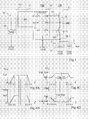
- FIG. 1 schematically and partially illustrates, a classic example of a linear regulator of a voltage Vout across a load (LD) 1.
- the regulator includes a transistor P 2 channel MOS whose source is connected to a rail high voltage supply Vdd and the drain of which constitutes the output terminal OUT of the regulator.
- Load 1 is connected between the OUT terminal and a low or voltage supply rail GND reference or mass.
- the transistor 2 works in regime linear, that is to say that we use its transconductance to vary its output current according to the voltage of control applied to its grid G.
- the control voltage of the grid G is regulated as a function of the voltage Vout at the terminals of load 1. Regulation is carried out by a comparator differential 3 comprising an input / output stage 4 and a stage 5.
- the input / output stage 4 comprises two branches differentials each with a P channel MOS transistor 61, 62 connected in series with an N-channel MOS transistor 63, 64.
- the sources of transistors 61 and 62 are connected to a output terminal of a current source 60 including one terminal input is connected to the high Vdd power supply.
- the sources of transistors 63 and 64 are connected to the GND low power supply.
- the gates of the transistors 63 and 64 are interconnected.
- a branch 61-63 constitutes an input branch, while the other branch 62-64 constitutes an output branch.
- the transistor 61 of the input branch receives a DC voltage setpoint constant Vreg supplied by a voltage generator 8, connected between the gate of transistor 61 and GND ground.
- the grid of transistor 63 is connected to its drain, i.e. also to the drain of transistor 61.
- the gate of transistor 63 receives the voltage Vout at the terminals of load 1 by a connection to the output terminal OUT of the regulator, possibly to a socket through a resistance bridge.
- Connection point 65 of the drains of the transistors 62 and 64 constitutes the output of the input / output stage 4 of the comparator 3.
- the output stage 5 consists of the connection in series, between the high Vdd and low GND power supplies, of a generally resistive impedance 9 (R) and of a MOS transistor channel N 10.
- the connection point of impedance 9 and the transistor 10 constitutes the output terminal of the differential comparator 3 connected to the gate G of the regulation transistor 2.
- the gate of transistor 10 is connected to point 65 of the branch input / output differential 62-64.
- the regulator also has an impedance (C) 11, generally capacitive, intended to stabilize the voltage of Vout exit.
- C impedance
- FIGS. 2A-2C illustrate, by timing diagrams, an example of variation as a function of time t of the setpoint of Vreg voltage across source 8, output voltage Vout at the terminals of the load 1, and of the voltage Vds between the drain and source terminals of transistor 2.
- the voltage generator is validated constant constant 8 so that it delivers a setpoint of stable non-zero nominal regulation Vref up to an instant t1 circuit extinction.
- the 3 force differential comparator then, as illustrated in FIG. 2B, the output voltage Vout to follow the regulation voltage Vreg and align with the reference level Vref.
- the voltage Vout is then regulated by stably at level Vref by gate control up to the instant t1 of circuit extinction or standby. This regulation is carried out by a command in linear mode of the transistor 2 which is used as a variable transconductance whose output current depends on the control voltage on grid G.
- the load 1 must be supplied with a voltage level of around 3.3 to 5.5 volts. Such a value is relatively high compared to the 2.4 to 2.8 volts maximum voltage that can hold the components (in particular the MOS 2 transistor) used in standard integration technology streams. However, during periods of load 1 extinction, the MOS transistor 2 must hold the voltage Vdd across its terminals.
- bipolar regulating transistor which has the advantage of requiring less integration area compared to the specific MOS, in particular because it can more easily be vertically integrated into a substrate of silicon.
- a bipolar transistor poses many problems.
- BiCMOS sector which is more complex than the MOS sector.
- a bipolar regulating transistor leads to higher waste voltages than a transistor MOS with a narrower range of linearity. This is particularly disadvantageous in the case of devices of the type portable for which it is desirable to reduce the most possible waste voltage, that is to make it, to preferably less than 200 mV.
- the present invention aims to propose a regulator linear which overcomes the drawbacks of known circuits.
- the present invention aims in particular to propose a linear regulator which has a reduced waste voltage.
- the present invention aims to propose such a regulator which can be manufactured using a standard MOS die.
- this invention provides a linear regulator comprising a stage of output including first and second channel MOS transistors P, connected in series between a first supply terminal DC and an output terminal providing a voltage of regulated output, and a control circuit for the first and second transistors capable of providing first and second signals of control according to the output voltage and the voltage at midpoint of the serial connection.
- the control circuit includes an input / output circuit and a reference circuit, the input / output circuit comprising a first input, receiving a first voltage setpoint supplied by said reference circuit; a second input, connected at said output terminal; a third entry receiving a second voltage setpoint supplied by said circuit reference; a fourth input connected to said midpoint; a first output connected to the gate of the first transistor ; and a second output connected to the gate of the second transistor.
- the input / output circuit is a double differential comparator with four inputs and two outputs.
- the input / output circuit includes first and second comparators differential with two inputs and two outputs, the terminals input of the first differential comparator being the first and second input terminals of the input / output circuit and its output being the second output of said input / output circuit; and the input terminals of the second differential comparator being the third and fourth input terminals of said input / output circuit and its exit being the first exit.
- the first differential comparator has an input / output stage and an output stage, said input / output stage comprising two differential branches each of which includes a transistor P channel MOS connected in series with a first transistor N-channel MOS, sources of P-channel transistors being interconnected to an output terminal of a source of current of which one input terminal is connected to said terminal DC power sources, the sources of the first transistors N channel being interconnected to a ground terminal, the grids said first N-channel MOS transistors being interconnected, the gates of the P channel transistors constituting the first and second input terminals of the input / output circuit, the gate of the first N-channel MOS transistor of the branch comprising the first input being connected to its drain, the connection point of the transistors drains complementary to the other branch being connected to the grid of a second N-channel MOS transistor connected, in said stage of output, in series between the supply terminals, with a first impedance, the midpoint of the serial connection of said first impedance and the second transistor constituting the output terminal
- the second differential comparator has two differential branches symmetrical each consisting of the connection in series of a second impedance, and of a third MOS transistor to N channel, respectively, the sources of the third transistors with N channel being interconnected to the drain of a fourth N-channel MOS transistor whose source is connected to the ground, the gate of the fourth N-channel transistor being connected to the gate of the second N-channel MOS transistor of the stage of output of the first differential comparator.
- FIG. 3 represents, in the form of a block diagram, a linear regulator 30 according to one embodiment of the present invention.
- the regulator 30 has an output stage 31 consisting of the series connection, between a power rail high Vdd and one output terminal OUT, of two transistors P channel MOS 32 and 33.
- the output terminal OUT is intended for be connected to a first load supply terminal (LD) 1, a second supply terminal of which is connected to a GND low or ground power rail.
- LD load supply terminal
- linear regulator 30 also preferably includes a stabilization impedance 11, for example a capacitor C.
- the regulation of the voltage Vout at the terminals of the load 1, i.e. on the output terminal OUT, is carried out by modulating control signals of the grids G1 and G2 of the transistors 32 and 33, respectively, so as to modify their transconductance.
- the control signals of the output stage 31 are produced by a control circuit 35.
- Circuit 35 modulates the control signal of the gate G1 of the transistor 32 so as to regulate the voltage at the midpoint MID of the series connection transistors 32 and 33 of the output stage 31. It modulates also the control signal of the gate G2 of the transistor 32 so as to regulate the output voltage Vout.
- Circuit 35 has an input / output stage (IN / OUT) 36 intended for producing the control signals and a reference stage (REF) 37.
- the input / output stage 36 includes four input terminals I1, 12, 13 and 14 and two output terminals 01 and 02.
- Terminal I1 receives a voltage regulation set point V1 of the Vout exit.
- Terminal I2 receives the output voltage Vout.
- the terminal I3 receives a regulation voltage setpoint V2 from the voltage at midpoint MID.
- Terminal I4 receives the voltage Vmid from the midpoint MID by a direct connection to this point.
- the output terminals O1 and 02 are respectively connected to the grids G1, G2.
- FIGS. 4A, 4B, 4C and 4D respectively illustrate, by chronograms, the variation as a function of time t of the regulation setpoint V1 of the output voltage Vout of regulator 30 of FIG. 3, of the output voltage Vout, of the V2 midpoint voltage regulation setpoint and of the current voltage Vmid at the midpoint MID, that is to say the drain voltage of transistor 32.
- the output voltage Vout follows, from at time t10, the first setpoint V1 until it stabilizes at the instant t11 at the nominal value Vref.
- the voltage Vmid at midpoint MID illustrated in FIG. 4D, decreases by controlled way of half the high feed (Vdd / 2) up to the stable value (Vdd-Vref) / 2.
- Vdd / 2 the stable value
- Vdd-Vref stable value
- the control circuit 35 ensures that any possible fluctuation in power at load level 1 results in a variation of the setpoints V1 and V2 so as to restore the nominal speed and distribute the power variation symmetrically on both power transistors 32 and 33.
- the control circuit 35 ensures that neither of the two transistors 32 and / or 33 does not face tension excessive drain / source.
- FIG. 4 shows boot ramps and of different respective slope extinction. More specifically, we represented a faster extinction (t12-t13) than priming (t10-t11).
- the slope of the ramps depends technical performance of the circuits and in particular of the ability of the control circuit 35 to track, transform and transmit, the variation of the first setpoint V1.
- the hills may be faster or slower than shown. In in addition, they can be symmetrical or present an asymmetry opposite to that shown, that is to say that the priming can be faster than extinction.
- FIG. 5 illustrates, schematically and partially, the structure of an embodiment of the input / output stage 36 a control circuit 35 of an output stage 31 of a regulator 30 according to the present invention.
- Input / output circuit 36 with four inputs and two outputs is a differential comparator. More specifically, circuit 36 consists of the association of a first differential comparator 50 and a second differential comparator 51 intertwined as follows.
- the first comparator 50 delimited by a frame in dotted in Figure 5, is intended to regulate the voltage of Vout output from the first setpoint V1.
- the comparator 50 therefore has a structure similar to that of a comparator known differential such as comparator 3 described in relation with Figure 1. For clarity, the structure of the comparator 50 is described below using the same references as in figure 1.
- Comparator 50 has an input / output stage 4 and an output stage 5.
- Stage 4 comprises two differential branches each comprising a P-channel MOS transistor 61, 62 connected in series with an N-channel MOS transistor 63, 64.
- the sources of transistors 61 and 62 are connected to a terminal of output of a current source 60 of which an input terminal is connected to the high Vdd power supply.
- the sources of the transistors 63 and 64 are connected to the GND low power supply.
- Grates transistors 63 and 64 are interconnected.
- the grid of transistor 61 constitutes the terminal I1 and receives the setpoint V1.
- the gate of transistor 63 is connected to its drain, i.e. also to the drain of transistor 61.
- the gate of transistor 62 constitutes the terminal I2 and receives the current voltage Vout aux load 1 terminals by connection to the OUT output terminal of the regulator.
- the connection point 65 of the drains of the transistors 62 and 64 constitute the output of the input / output stage 4 of comparator 50.
- the output stage 5 consists of the connection in series, between the high Vdd supply and GND ground, of a impedance 9, preferably resistive (R), and a MOS transistor N channel 10.
- the connection point of impedance 9 and transistor 10 constitutes the output terminal 02 providing the control signal of the gate G2 of the transistor 33.
- the gate of transistor 10 is connected to midpoint 65 of the branch differential 62-64 of the input stage 4.
- the second differential comparator 51 is intended for control the voltage regulation at the MID point. He gives on the output terminal 01 the control signal from the gate G1.
- the second comparator 51 has two differential branches symmetrical, each consisting of the series connection an impedance 52, 53, preferably resistive, and a N-channel MOS transistor 54, 55, respectively.
- the sources of transistors 54 and 55 are connected to the drain of a transistor N-channel MOS 56 whose source is connected to GND ground.
- the gate of transistor 56 is connected to output 65 of the stage input / output 4 and to the gate of transistor 10 of the stage of output 5 of the first differential comparator 50. Consequently, the operating point of the second differential comparator 51 depends on that of the output stage 5 of the first comparator differential 50.
- FIG. 6 represents, schematically and partially, an embodiment of a generator 37 of the setpoints V1 and V2.
- the reference circuit 37 is, according to one embodiment of the present invention, a resistive voltage divider.
- the resistive divider has the series connection between the high Vdd and low GND power rails of three resistors 71, 72 and 73.
- the connection point 74 of the resistors 72 and 73 is the output terminal of a differential comparator 75 with two inputs and one output, for example similar to comparator 3 of figure 1.
- the non-inverting input terminal of comparator 75 receives the Vreg regulation setpoint from the output voltage Vout of regulator 30, for example, by a connection to the source 38.
- the inverting input terminal of the comparator 75 is connected to the output terminal 74.
- the present invention advantageously provides a regulator linear power fully achievable by a die Low-voltage standard MOS with small dimensions. Indeed, replacement of the high-voltage regulator MOS transistor known by two low voltage transistors reduces the integration surface. In addition, the increased surface area of the control part 35 with respect to the control circuit of a known regulator is negligible compared to the surface gain related to the change of power switch.
- the linear regulator according to this invention has a lower waste voltage than known regulators.
- Vdd the high supply voltage
- each transistor 32 and 33 of the output stage 31 of the linear regulator 30 of the present invention is a standard MOS transistor suitable for holding a drain / source voltage of approximately 2.5 volts.
- the regulator waste voltage is then reduced to values of the order of 200 mV.
- the present invention is capable of various variations and modifications that will appear to humans art.
- the capacitor C (impedance 11) stabilization of the output voltage Vout has been described as functionally part of the regulator linear 30.
- the value of the capacitance of the capacitor C is relatively high and varies depending on the application, that is to say of the charge 1.
- the capacitor C is therefore, preferably made outside a circuit chip integrated with the regulator assembly 30, and is mounted directly in parallel on the load 1.
- the man of the trade will be able to modify the characteristics of the various components to the sector used.
Landscapes
- Engineering & Computer Science (AREA)
- Physics & Mathematics (AREA)
- Microelectronics & Electronic Packaging (AREA)
- Electromagnetism (AREA)
- General Physics & Mathematics (AREA)
- Radar, Positioning & Navigation (AREA)
- Automation & Control Theory (AREA)
- Nonlinear Science (AREA)
- Continuous-Control Power Sources That Use Transistors (AREA)
Abstract
Description
Claims (6)
- Régulateur linéaire comportant un étage de sortie (31) comprenant des premier et second transistors MOS à canal P (32, 33), connectés en série entre une première borne d'alimentation continue (Vdd) et une borne de sortie (OUT) fournissant une tension de sortie régulée (Vout), et un circuit de commande (35) des premier et second transistors propre à leur fournir des premier et second signaux de commande en fonction de la tension de sortie et de la tension au point milieu (MID) de la connexion en série.
- Régulateur selon la revendication 1, caractérisé en ce que le circuit de commande (35) comprend un circuit d'entrée/sortie (36) et un circuit de référence (37), le circuit d'entrée/sortie comportant :une première entrée (I1), recevant une première consigne de tension (V1) fournie par ledit circuit de référence ;une deuxième entrée (I2), connectée à ladite borne de sortie (OUT) ;une troisième entrée (I3) recevant une seconde consigne de tension (V2) fournie par ledit circuit de référence ;une quatrième entrée (I4) connectée audit point milieu (MID) ;une première sortie (01) connectée à la grille (G1) du premier transistor (32) ; etune deuxième sortie (02) connectée à la grille (G2) du deuxième transistor (33).
- Régulateur selon la revendication 2, caractérisé en ce que le circuit d'entrée/sortie (36) est un double comparateur différentiel à quatre entrées et deux sorties.
- Régulateur selon la revendication 2 ou 3, caractérisé en ce que le circuit d'entrée/sortie (36) comporte des premier (50) et second (51) comparateurs différentiels à deux entrées et deux sorties, les bornes d'entrée du premier comparateur différentiel étant les première (I1) et deuxième (I2) bornes d'entrée du circuit d'entrée/sortie et sa sortie étant la deuxième sortie (O2) dudit circuit d'entrée/sortie ; et les bornes d'entrée du second comparateur différentiel étant les troisième (13) et quatrième (14) bornes d'entrée dudit circuit d'entrée/sortie et sa sortie en étant la première sortie (01).
- Régulateur selon la revendication 4, caractérisé en ce que le premier comparateur différentiel (50) comporte un étage d'entrée/sortie (4) et un étage de sortie (5), ledit étage d'entrée/sortie comportant deux branches différentielles dont chacune comprend un transistor MOS à canal P (61, 62) connecté en série avec un premier transistor MOS à canal N (63, 64), les sources des transistors à canal P étant interconnectées à une borne de sortie d'une source de courant (60) dont une borne d'entrée est reliée à ladite borne d'alimentation continue (Vdd), les sources des premiers transistors à canal N étant interconnectées à une borne de masse (GND), les grilles desdits premiers transistors MOS à canal N étant interconnectées, les grilles des transistors à canal P constituant les première (I1) et deuxième (12) bornes d'entrée du circuit d'entrée/sortie (36), la grille du premier transistor MOS à canal N de la branche (61-63) comportant la première entrée étant connectée à son drain, le point milieu (65) de connexion des drains des transistors complémentaires de l'autre branche (62-64) étant relié à la grille d'un deuxième transistor MOS à canal N (10) connecté, dans ledit étage de sortie (5), en série entre les bornes d'alimentation, avec une première impédance (9), le point milieu de la connexion en série de ladite première impédance et du deuxième transistor constituant la borne de sortie (02) dudit premier comparateur différentiel.
- Régulateur selon la revendication 5, caractérisé en ce que le second comparateur différentiel (51) comporte deux branches différentielles symétriques constituées chacune de la connexion en série d'une seconde impédance (52, 53), et d'un troisième transistor MOS à canal N (54, 55), respectivement, les sources des troisièmes transistors à canal N étant connectées au drain d'un quatrième transistor MOS à canal N (56) dont la source est connectée à la masse (GND), la grille du quatrième transistor à canal N étant connectée à la grille du deuxième transistor MOS à canal N (10) de l'étage de sortie (5) du premier comparateur différentiel (50).
Applications Claiming Priority (2)
| Application Number | Priority Date | Filing Date | Title |
|---|---|---|---|
| FR0208624A FR2842316A1 (fr) | 2002-07-09 | 2002-07-09 | Regulateur de tension lineaire |
| FR0208624 | 2002-07-09 |
Publications (2)
| Publication Number | Publication Date |
|---|---|
| EP1380913A1 true EP1380913A1 (fr) | 2004-01-14 |
| EP1380913B1 EP1380913B1 (fr) | 2017-11-22 |
Family
ID=29725296
Family Applications (1)
| Application Number | Title | Priority Date | Filing Date |
|---|---|---|---|
| EP03300056.3A Expired - Lifetime EP1380913B1 (fr) | 2002-07-09 | 2003-07-09 | Régulateur de tension linéaire |
Country Status (3)
| Country | Link |
|---|---|
| US (1) | US6894467B2 (fr) |
| EP (1) | EP1380913B1 (fr) |
| FR (1) | FR2842316A1 (fr) |
Families Citing this family (17)
| Publication number | Priority date | Publication date | Assignee | Title |
|---|---|---|---|---|
| US8315588B2 (en) * | 2004-04-30 | 2012-11-20 | Lsi Corporation | Resistive voltage-down regulator for integrated circuit receivers |
| JP2006006004A (ja) * | 2004-06-16 | 2006-01-05 | Ricoh Co Ltd | 昇降圧型dc−dcコンバータ |
| EP1669831A1 (fr) * | 2004-12-03 | 2006-06-14 | Dialog Semiconductor GmbH | Étape de sortie d'un régulateur de voltage avec transistors MOS à basse tension |
| EP1891741A4 (fr) | 2005-06-08 | 2011-08-24 | Powercast Corp | Alimentation electrique de dispositif a recueil d'energie radiofrequence |
| US20090102296A1 (en) * | 2007-01-05 | 2009-04-23 | Powercast Corporation | Powering cell phones and similar devices using RF energy harvesting |
| DE102007023652B4 (de) * | 2007-05-22 | 2013-08-14 | Austriamicrosystems Ag | Spannungsregler und Verfahren zur Spannungsregelung |
| US20090079406A1 (en) * | 2007-09-26 | 2009-03-26 | Chaodan Deng | High-voltage tolerant low-dropout dual-path voltage regulator with optimized regulator resistance and supply rejection |
| US20100109435A1 (en) * | 2008-09-26 | 2010-05-06 | Uti Limited Partnership | Linear Voltage Regulator with Multiple Outputs |
| US8352036B2 (en) * | 2009-01-19 | 2013-01-08 | Anthony DiMarco | Respiratory muscle activation by spinal cord stimulation |
| US9035626B2 (en) * | 2010-08-18 | 2015-05-19 | Volterra Semiconductor Corporation | Switching circuits for extracting power from an electric power source and associated methods |
| DE102011053042A1 (de) | 2011-08-26 | 2013-02-28 | Verbindungstechnik und Metallverarbeitungs GmbH Seifart | Sortierfach zum Sortieren von Briefpost |
| US9831764B2 (en) * | 2014-11-20 | 2017-11-28 | Stmicroelectronics International N.V. | Scalable protection voltage generator |
| FR3032309B1 (fr) * | 2015-02-02 | 2017-06-23 | St Microelectronics Alps Sas | Circuit de regulation de tension adapte aux fortes et faibles puissances |
| CN117767593A (zh) | 2017-09-01 | 2024-03-26 | 鲍尔卡斯特公司 | 自动rf功率传输和单天线能量收集的方法、系统和装置 |
| US10763687B2 (en) | 2017-12-04 | 2020-09-01 | Powercast Corporation | Methods, systems, and apparatus for wireless recharging of battery-powered devices |
| EP3503334B1 (fr) * | 2017-12-20 | 2022-06-15 | Aptiv Technologies Limited | Unité d'alimentation électrique pour un dispositif électronique |
| DE102021106815B4 (de) | 2021-01-06 | 2023-06-01 | Taiwan Semiconductor Manufacturing Company, Ltd. | Stromversorgungsgenerator und betriebsverfahren dafür |
Citations (3)
| Publication number | Priority date | Publication date | Assignee | Title |
|---|---|---|---|---|
| US6104179A (en) * | 1998-07-23 | 2000-08-15 | Nec Corporation | Low-power consumption noise-free voltage regulator |
| EP1089154A1 (fr) * | 1999-10-01 | 2001-04-04 | STMicroelectronics SA | Régulateur linéaire à sélection de la tension de sortie |
| US20010007537A1 (en) * | 2000-01-07 | 2001-07-12 | Kabushiki Kaisha Toshiba | Data transfer circuit |
Family Cites Families (5)
| Publication number | Priority date | Publication date | Assignee | Title |
|---|---|---|---|---|
| JP3405871B2 (ja) * | 1995-11-28 | 2003-05-12 | 富士通株式会社 | 直流−直流変換制御回路および直流−直流変換装置 |
| FR2755317B1 (fr) * | 1996-10-25 | 1999-01-15 | Sgs Thomson Microelectronics | Regulateur de tension a generation interne d'un signal logique |
| FR2768527B1 (fr) * | 1997-09-18 | 2000-07-13 | Sgs Thomson Microelectronics | Regulateur de tension |
| US6429633B1 (en) * | 1998-08-28 | 2002-08-06 | Matsushita Electric Industrial Co., Ltd. | Switching regulator and LSI system |
| DE69927004D1 (de) * | 1999-06-16 | 2005-10-06 | St Microelectronics Srl | BICMOS / CMOS Spannungsregler mit kleiner Verlustspannung |
-
2002
- 2002-07-09 FR FR0208624A patent/FR2842316A1/fr active Pending
-
2003
- 2003-07-07 US US10/614,380 patent/US6894467B2/en not_active Expired - Lifetime
- 2003-07-09 EP EP03300056.3A patent/EP1380913B1/fr not_active Expired - Lifetime
Patent Citations (3)
| Publication number | Priority date | Publication date | Assignee | Title |
|---|---|---|---|---|
| US6104179A (en) * | 1998-07-23 | 2000-08-15 | Nec Corporation | Low-power consumption noise-free voltage regulator |
| EP1089154A1 (fr) * | 1999-10-01 | 2001-04-04 | STMicroelectronics SA | Régulateur linéaire à sélection de la tension de sortie |
| US20010007537A1 (en) * | 2000-01-07 | 2001-07-12 | Kabushiki Kaisha Toshiba | Data transfer circuit |
Also Published As
| Publication number | Publication date |
|---|---|
| US6894467B2 (en) | 2005-05-17 |
| US20040008015A1 (en) | 2004-01-15 |
| EP1380913B1 (fr) | 2017-11-22 |
| FR2842316A1 (fr) | 2004-01-16 |
Similar Documents
| Publication | Publication Date | Title |
|---|---|---|
| EP1380913B1 (fr) | Régulateur de tension linéaire | |
| EP0731562B1 (fr) | Circuit logique à étage différentiel | |
| EP0733961B1 (fr) | Générateur de courant de référence en technologie CMOS | |
| FR2755318A1 (fr) | Circuit regulateur et dispositif a circuit integre a semi-conducteur le comprenant | |
| FR2677793A1 (fr) | Circuit pour produire une tension d'alimentation interne. | |
| FR2819064A1 (fr) | Regulateur de tension a stabilite amelioree | |
| FR2637703A1 (fr) | Circuit regulateur stabilise a faible tension de mise hors fonction | |
| FR2912013A1 (fr) | Dispositif de generation de courant de polarisation ayant un coefficient de temperature ajustable. | |
| EP1326154B1 (fr) | Pompe à charge à très large plage de tension de sortie | |
| FR3032309A1 (fr) | Circuit de regulation de tension adapte aux fortes et faibles puissances | |
| FR3102580A1 (fr) | Régulateur de tension | |
| EP1089154A1 (fr) | Régulateur linéaire à sélection de la tension de sortie | |
| FR2819652A1 (fr) | Regulateur de tension a rendement ameliore | |
| FR2854008A1 (fr) | Amplificateur differentiel a correction de mode commun | |
| EP1916762B1 (fr) | Oscillateur à quartz asservi en amplitude avec domaine étendu de tension et de température | |
| FR2896051A1 (fr) | Regulateur de tension serie a faible tension d'insertion | |
| FR2957161A1 (fr) | Circuit interne de tension d'alimentation d'un circuit integre | |
| EP0723160A1 (fr) | Circuit de détection de tension compensé en technologie et en température | |
| FR2835664A1 (fr) | Procede de generation d'une rampe de tension aux bornes d'un condensateur, et dispositif electronique correspondant, en particulier pour une alimentation a decoupage d'un telephone mobile cellulaire | |
| WO2002045261A2 (fr) | Ensemble commandable de sources de courant | |
| EP1040580A1 (fr) | Amplificateur de sortie cmos independant de la temperature, de la tension d'alimentation et de la qualite de fabrication de ses transistors | |
| FR2969328A1 (fr) | Circuit de generation d'une tension de reference sous une faible tension d'alimentation | |
| FR2818762A1 (fr) | Regulateur de tension a gain statique en boucle ouverte reduit | |
| EP0050583B1 (fr) | Convertisseur d'une tension alternative en un courant continu et circuit d'oscillateur comportant ce convertisseur | |
| EP1326155A1 (fr) | Générateur de tension de référence à performances améliorées |
Legal Events
| Date | Code | Title | Description |
|---|---|---|---|
| PUAI | Public reference made under article 153(3) epc to a published international application that has entered the european phase |
Free format text: ORIGINAL CODE: 0009012 |
|
| AK | Designated contracting states |
Kind code of ref document: A1 Designated state(s): AT BE BG CH CY CZ DE DK EE ES FI FR GB GR HU IE IT LI LU MC NL PT RO SE SI SK TR |
|
| AX | Request for extension of the european patent |
Extension state: AL LT LV MK |
|
| 17P | Request for examination filed |
Effective date: 20040714 |
|
| AKX | Designation fees paid |
Designated state(s): DE FR GB IT |
|
| 17Q | First examination report despatched |
Effective date: 20100409 |
|
| REG | Reference to a national code |
Ref country code: DE Ref legal event code: R079 Ref document number: 60350783 Country of ref document: DE Free format text: PREVIOUS MAIN CLASS: G05F0003240000 Ipc: G05F0001560000 |
|
| GRAP | Despatch of communication of intention to grant a patent |
Free format text: ORIGINAL CODE: EPIDOSNIGR1 |
|
| STAA | Information on the status of an ep patent application or granted ep patent |
Free format text: STATUS: GRANT OF PATENT IS INTENDED |
|
| RIC1 | Information provided on ipc code assigned before grant |
Ipc: G05F 1/56 20060101AFI20170428BHEP Ipc: G05F 3/24 20060101ALI20170428BHEP Ipc: G05F 3/26 20060101ALI20170428BHEP |
|
| INTG | Intention to grant announced |
Effective date: 20170530 |
|
| GRAS | Grant fee paid |
Free format text: ORIGINAL CODE: EPIDOSNIGR3 |
|
| GRAA | (expected) grant |
Free format text: ORIGINAL CODE: 0009210 |
|
| STAA | Information on the status of an ep patent application or granted ep patent |
Free format text: STATUS: THE PATENT HAS BEEN GRANTED |
|
| AK | Designated contracting states |
Kind code of ref document: B1 Designated state(s): DE FR GB IT |
|
| REG | Reference to a national code |
Ref country code: GB Ref legal event code: FG4D Free format text: NOT ENGLISH |
|
| REG | Reference to a national code |
Ref country code: DE Ref legal event code: R096 Ref document number: 60350783 Country of ref document: DE |
|
| REG | Reference to a national code |
Ref country code: DE Ref legal event code: R097 Ref document number: 60350783 Country of ref document: DE |
|
| PG25 | Lapsed in a contracting state [announced via postgrant information from national office to epo] |
Ref country code: IT Free format text: LAPSE BECAUSE OF FAILURE TO SUBMIT A TRANSLATION OF THE DESCRIPTION OR TO PAY THE FEE WITHIN THE PRESCRIBED TIME-LIMIT Effective date: 20171122 |
|
| PLBE | No opposition filed within time limit |
Free format text: ORIGINAL CODE: 0009261 |
|
| STAA | Information on the status of an ep patent application or granted ep patent |
Free format text: STATUS: NO OPPOSITION FILED WITHIN TIME LIMIT |
|
| 26N | No opposition filed |
Effective date: 20180823 |
|
| REG | Reference to a national code |
Ref country code: DE Ref legal event code: R119 Ref document number: 60350783 Country of ref document: DE |
|
| GBPC | Gb: european patent ceased through non-payment of renewal fee |
Effective date: 20180709 |
|
| PG25 | Lapsed in a contracting state [announced via postgrant information from national office to epo] |
Ref country code: GB Free format text: LAPSE BECAUSE OF NON-PAYMENT OF DUE FEES Effective date: 20180709 Ref country code: DE Free format text: LAPSE BECAUSE OF NON-PAYMENT OF DUE FEES Effective date: 20190201 Ref country code: FR Free format text: LAPSE BECAUSE OF NON-PAYMENT OF DUE FEES Effective date: 20180731 |