EP1380867B1 - Steckverbindergehäuse für Lichtwellenleiter - Google Patents
Steckverbindergehäuse für Lichtwellenleiter Download PDFInfo
- Publication number
- EP1380867B1 EP1380867B1 EP03015062A EP03015062A EP1380867B1 EP 1380867 B1 EP1380867 B1 EP 1380867B1 EP 03015062 A EP03015062 A EP 03015062A EP 03015062 A EP03015062 A EP 03015062A EP 1380867 B1 EP1380867 B1 EP 1380867B1
- Authority
- EP
- European Patent Office
- Prior art keywords
- connector housing
- optical
- laser
- optical waveguide
- housing
- Prior art date
- Legal status (The legal status is an assumption and is not a legal conclusion. Google has not performed a legal analysis and makes no representation as to the accuracy of the status listed.)
- Expired - Lifetime
Links
- 230000003287 optical effect Effects 0.000 title claims description 46
- 238000003466 welding Methods 0.000 claims description 20
- 239000004033 plastic Substances 0.000 claims description 17
- 229920003023 plastic Polymers 0.000 claims description 17
- 238000000034 method Methods 0.000 claims description 14
- 230000005540 biological transmission Effects 0.000 claims description 10
- 239000000463 material Substances 0.000 claims description 9
- 238000001746 injection moulding Methods 0.000 claims description 4
- 238000005253 cladding Methods 0.000 claims description 3
- 239000011248 coating agent Substances 0.000 claims 1
- 238000000576 coating method Methods 0.000 claims 1
- 239000013307 optical fiber Substances 0.000 description 11
- 239000000835 fiber Substances 0.000 description 8
- 238000005304 joining Methods 0.000 description 8
- 238000010521 absorption reaction Methods 0.000 description 4
- 230000008878 coupling Effects 0.000 description 4
- 238000010168 coupling process Methods 0.000 description 4
- 238000005859 coupling reaction Methods 0.000 description 4
- 230000005855 radiation Effects 0.000 description 4
- 230000000295 complement effect Effects 0.000 description 3
- 238000004519 manufacturing process Methods 0.000 description 3
- 239000000975 dye Substances 0.000 description 2
- 239000000945 filler Substances 0.000 description 2
- 238000010438 heat treatment Methods 0.000 description 2
- 239000002184 metal Substances 0.000 description 2
- 229920000642 polymer Polymers 0.000 description 2
- 239000004952 Polyamide Substances 0.000 description 1
- 239000000654 additive Substances 0.000 description 1
- 238000001514 detection method Methods 0.000 description 1
- 230000000694 effects Effects 0.000 description 1
- 239000003292 glue Substances 0.000 description 1
- 239000000155 melt Substances 0.000 description 1
- 238000002844 melting Methods 0.000 description 1
- 230000008018 melting Effects 0.000 description 1
- 239000013308 plastic optical fiber Substances 0.000 description 1
- 238000004023 plastic welding Methods 0.000 description 1
- 229920002647 polyamide Polymers 0.000 description 1
- 238000004886 process control Methods 0.000 description 1
- 239000011253 protective coating Substances 0.000 description 1
- 230000008961 swelling Effects 0.000 description 1
- 239000012815 thermoplastic material Substances 0.000 description 1
- 238000002834 transmittance Methods 0.000 description 1
- 239000012780 transparent material Substances 0.000 description 1
- 238000002604 ultrasonography Methods 0.000 description 1
Images

Classifications
-
- G—PHYSICS
- G02—OPTICS
- G02B—OPTICAL ELEMENTS, SYSTEMS OR APPARATUS
- G02B6/00—Light guides; Structural details of arrangements comprising light guides and other optical elements, e.g. couplings
- G02B6/24—Coupling light guides
- G02B6/36—Mechanical coupling means
- G02B6/38—Mechanical coupling means having fibre to fibre mating means
- G02B6/3807—Dismountable connectors, i.e. comprising plugs
- G02B6/3887—Anchoring optical cables to connector housings, e.g. strain relief features
- G02B6/3888—Protection from over-extension or over-compression
Definitions
- the invention relates to a connector housing for optical fibers, which is made of plastic and in which at least one optical waveguide is stationarily positioned and mechanically fixed.
- electro-optical transmitters such as LED's and laser diodes and electro-optical receivers, such as photodiodes and phototransistors
- electro-optical receivers such as photodiodes and phototransistors
- two separate optical fibers eg Problem that the faces of the photoconductive fibers must be brought to the corresponding transmitting or receiving surfaces very accurately in position and held.
- the optical axes must be brought precisely to coincide and connect very close to each other, d. H. they must be accurately positioned both in the radial and in the axial direction.
- the end of the optical waveguide is initially assembled with a tube, called a ferrule (also called insert) in the known optical connectors.
- a ferrule also called insert
- This standard contact ie the ferrule with the optical waveguide attached to it, is then subsequently mounted in a typically made of at least two plastic parts connector housing, so positioned and fixed. Accordingly, a receptacle for the standard contact and means for securing the standard contact in the receptacle must be provided in the connector housing.
- Such optical connectors are often designed as modules that can be integrated in external connectors.
- the EP 0 590 394 A1 shows a coupling arrangement in which an optical fiber in a ferrule of plastic fixed and the ferrule is then fixed in an adjustable relative to a housing adjustment sleeve.
- the laser plastic welding in the transmission method is based on the relatively lower absorption of laser radiation in a first joint partner, here: the ferrule through which the laser radiation therefore reaches the other joint partner, here: the plastic jacket of the optical waveguide, which has a relatively higher absorption so that it converts the laser beam into heat, whereby the plastic melts at the joining surface.
- the WO 01/88583 A1 discloses an apparatus for laser welding a ferrule of an optical waveguide to the optical waveguide, the ferrule being made more transparent than the protective coating of the optical waveguide.
- Object of the present invention is to provide a particularly improved in terms of parts and space economics connector housing of the type mentioned.
- the connector housing with the same interface optical component / optical fiber moreover compact than before fail, since no recording for a standard contact must be provided, but the housing can be minimized application specific in its space.
- the connector housing may be formed as an optical module, so for example realize a coupled optical waveguides optical transmitter / receiver unit, which itself - optionally together with other components and / or other modules - can be integrated in an outer connector with a complementary plug to a connector is fauxhegbar.
- a preferred embodiment can be achieved by providing in an outer wall of the connector housing at least one recess which opens the outer wall to a predetermined depth, so that the laser beam has access to the welding area lying behind by the outer wall remaining there with a defined wall thickness.
- the basic idea of the invention essentially only presupposes that - at least during the welding process - parts of the outer wall of the connector housing for laser light of the wavelength used are designed to be sufficiently transmissive. This allows a variety of design with respect to the properties / functions of the wall of the connector housing, in particular, a metallized or partially metallized plastic housing can be made with greater creative freedom than when using a conventional outer sheet metal part.
- an existing plastic bushing housing 1 in which the provided with a sheath of plastic optical fibers 2 and 3 are fixed.
- cylindrical bushings 4 and 5 are integrally formed on its front side, while on the end face 11 of the pin housing 6 according to Figure 4, 5 and 6, a complementary pin geometry is formed.
- recesses 7 existing, for material removal, d. H. to avoid Massaufkorufonne in the housing 1 and 6 serve. These recesses 7, which can vary greatly depending on the application, can be seen above all in FIGS. 2, 3 and 5.
- optical waveguides 2 and 3 are introduced in the assembly of, for example, the female housing 1 in the one-piece socket housing 1 so that the ends of the plastic fibers 2 and 3 substantially flat on the open end side 10 there (in the middle of the cylindrical bushings 4 and 5) lie.
- laser light having a wavelength in the so-called near infrared range 800 to 810 nm
- each optical waveguide 2 and 3 it is sufficient for each optical waveguide 2 and 3 to set a slightly oval, about three to four millimeters long welding point on the jacket of the optical waveguide 2 and 3 respectively.
- the laser is adjusted so that, for a given transmission, a weld still succeeds by a wall thickness of for example two to three millimeters through.
- These welding parameters are not adjusted in each case depending on the application-individual case, but it is advantageously the depth of the recess 8 so dimensioned that a defined wall thickness to the weld point of, in the example mentioned, two to three millimeters remains.
- the transmission through the socket housing 1 or the pin housing 6 depends - apart from the wall thickness - mainly from the plastic material and any additives, such as dyes or fillers from. Meanwhile, there are available dyes which appear black in the wavelength range of visible light but exhibit high transmittance of near infrared light. Black connector housings are thus readily possible according to the invention.
- the previous connector housings have been provided with an outer sheet metal part for EMC shielding in particular in applications that require a high data rate, for example in the automotive, in the EDP area or in consumer electronics.
- This conventional design of the shield is - possibly after the welding process - even in the connector housing according to the invention possible.
- the connector housing may advantageously be made in the so-called two-component injection molding.
- the connector housing then consists on the one hand of a laser-weldable, transparent to the laser light used material and, on the other hand, of a material with a different technical property, for example, EMC shielding.
- Another possibility is to injection-mold the entire connector housing from a single transparent material used for welding laser light, but then selectively metalize the outer wall 9.
- An advantageous variant is to produce the connector housing from a transparent to the laser light used for welding, for the light emitted by a transmitting diode light (for example, red, 650 nm) but impermeable material.
- This connector housing is laser weldable, but at the same time optical crosstalk of the transmitter and receiver elements is prevented.
Landscapes
- Physics & Mathematics (AREA)
- General Physics & Mathematics (AREA)
- Optics & Photonics (AREA)
- Optical Couplings Of Light Guides (AREA)
- Mechanical Coupling Of Light Guides (AREA)
Description
- Die Erfindung betrifft ein Steckverbindergehäuse für Lichtwellenleiter, das aus Kunststoff hergestellt ist und in dem mindestens ein Lichtwellenleiter ortsfest positioniert und mechanisch fixiert ist.
- Bei der Kopplung von elektrooptischen Sendern, wie zum Beispiel LED's und Laserdioden und elektrooptischen Empfängern, wie zum Beispiel Photodioden und Phototransistoren mittels einer lichtleitenden Faser, oder bei der optischen Verbindung von zwei getrennten Lichtwellenleitern (z. B. aus Kunststoff) miteinander, ergibt sich das Problem, dass die Stirnflächen der lichtleitenden Fasern zu den korrespondierenden Sende- oder Empfangsflächen sehr genau in Position gebracht und gehalten werden müssen. Dabei müssen die optischen Achsen präzise zur Deckung gebracht werden und sehr nahe aneinander anschließen, d. h. sie müssen sowohl in radialer als auch in axialer Richtung exakt positioniert werden.
- Um eine einwandfreie Ankopplung eines Lichtwellenleiters zu einem Sender oder zu einem Empfänger oder eine einwandfreie Kopplung Faser/Faser zu gewährleisten, wird bei den bekannten optischen Steckverbindungen das Ende des Lichtwellenleiters zunächst mit einem Röhrchen, einer so genannten Ferrule (auch Insert genannt) konfektioniert. Dieser Standardkontakt, also die Ferrule mit dem an ihr befestigten Lichtwellenleiter, wird erst anschließend in ein typischerweise aus mindestens zwei Kunststoffteilen bestehendes Steckverbindergehäuse montiert, also positioniert und fixiert. In dem Steckverbindergehäuse müssen dementsprechend eine Aufnahme für den Standardkontakt und Mittel zur Sicherung des Standardkontaktes in der Aufnahme vorgesehen werden. Derartige optische Steckverbindungen sind oft als in Außenstecker integrierbare Module ausgebildet.
- Für die beim Standardkontakt erforderliche Befestigung der Ferrule am Lichtwellenleiter bzw. für die anschließende Befestigung des Standardkontaktes in der jeweiligen Umgebung stehen verschiedene Techniken zur Verfügung:
- Aus der Offenlegungsschrift
DE 28 01 603 A1 ist ein Lichtwellenleiter mit einem Mantel aus thermoplastischem Material bekannt, bei dem an einem Ende eine Verbindungsklemme aus dem gleichen Material befestigt werden soll. Dazu wird vorgeschlagen, die beiden Teile primär mit Ultraschall, oder unter (nicht spezifizierter) Wärmewirkung, zu verschweißen. - In der
DE 195 29 527 C1 ist ein Verfahren zur Herstellung einer Faser-Ferrule-Verbindung beschrieben, bei dem eine Faser aus Kunststoff durch wärmebedingtes Aufquellen in einer Ferrule aus Kunststoff festgelegt werden soll. Indem der Mantelfläche der Ferrule zur Erhitzung eine Strahlung zugeführt wird und eine Ferrule verwendet wird, die mit Durchbrüchen von der Mantelfläche bis zur Lichtleiterfaser versehen ist, kann Wärme effektiv zugeführt werden. Die Wärmeenergie wird durch einen konzentrierten Licht- oder Heißluft-Strahl zugeführt, der durch die Durchbrüche unmittelbar an die Faser gelangt. Die Erhitzung wird nur bis zur Aufquelltemperatur, nicht bis zum Schmelzen, durchgeführt. - Die
EP 0 590 394 A1 zeigt eine Koppelanordnung, bei der eine Lichtwellenleiterfaser in einer Ferrule aus Kunststoff fixiert und die Ferrule anschließend in einer gegenüber einem Gehäuse justierbaren Justierhülse festgelegt wird. Durch eine zumindest punktweise Warmfügeverbindung, vorzugsweise (konventionelles) Laserverschweißen, gelingt es, eine Befestigung der Justierhülse am Gehäuse zu erzeugen, ohne im Zuge der dabei auftretenden Wärmebelastung die Qualität der vorherigen optischen Justierung wieder zu gefährden. - Schließlich ist es aus der
US-A-4 859 827 bekannt, eine Lichtwellenleiterfaser in eine Ferrule zu kleben und die Ferrule durch konventionelles Laserverschweißen im Durchschmelzverfahren an einer, typischerweise metallischen, Muffe zu befestigen. Um nicht durch die ganze Dicke der Muffe durchschmelzen zu müssen, wird vorgeschlagen, die Muffenwand, auf die die Laserstrahlung gerichtet ist, von außen her abzudünnen. - Aus der
DE 199 19 428 A1 ist es bekannt, die innovative Fügetechnik des Laser-Durchstrahlschweißens bei einer Ferrule aus Kunststoff anzuwenden, um sie direkt an einem Mantel des Lichtwellenleiters zu verschweißen. Das Laser-Kunststoffschweißen im Durchstrahlverfahren beruht auf der relativ geringeren Absorption von Laserstrahlung in einem ersten Fügepartner, hier: der Ferrule, durch den hindurch die Laserstrahlung deshalb den anderen Fügepartner, hier: den Kunststoff-Mantel des Lichtwellenleiters, erreicht, der eine relativ höhere Absorption aufweist, so dass er den Laserstrahl in Wärme umwandelt, wodurch der Kunststoff an der Fügefläche schmilzt. - In der Publikation "Fügen von Kunststoffen mit Diodenlasern verbessert die Nahtqualität", Maschinenmarkt Das Industriemagazin, 105 Nr. 17, 26. April 1999, Seiten 38 bis 42, wird, ohne Bezug auf Lichtwellenleiter oder Gehäuse als Fügepartner, in einem allgemeinen Kontext u. a. auf prozesstechnische Voraussetzungen beim Durchstrahlverfahren eingegangen, insbesondere werden das Erfordernis eines formschlüssigen Kontaktes zwischen den Fügeteilen und deren Fixierung zueinander, eine Prozessregelung mit Temperaturerfassung, sowie Verfahrensvarianten wie das simultane und kontinuierliche Schweißen diskutiert. Als Anwendungsbeispiel wird die Herstellung von Kunststofffenstern erwähnt.
- Schließlich werden in der Publikation "Laserschweißen von Polymerteilen Qualitätsverbesserung von Polymerteilen durch Laserschweißen", 5. (Int.) Kunststoff Sauganlagen Forum, 1998, Seiten 1 bis 12, wiederum ohne Bezug auf Lichtwellenleiter oder Gehäuse als Fügepartner, im Zusammenhang mit dem Durchstrahlverfahren u. a. die Absorptionscharakteristika insbesondere von Polyamid diskutiert. Es wird allgemein darauf hingewiesen, dass verschiedene Verbindungsgeometrien der Fügepartner zur Erzielung einer maximalen Wärmezufuhr im Verbindungsbereich möglich sind und es wird eine online Registrierung der Prozesstemperatur beim Schweißvorgang als unabdingbar bezeichnet.
- Die
WO 01/88583 A1 - Generell ist vor einer Anwendung des Durchstrahlverfahrens zu bedenken, dass dessen Einsatzmöglichkeiten im Allgemeinen sehr von der Fügenahtgeometrie, der Fügestrategie und der Absorption bzw. Transmission abhängen, die selbst wiederum u. a. vom Kunststofftyp, dem Füllstoff und der Wanddicke abhängt, so dass wesentlich auf die Gegebenheiten im Einzelfall abzustellen ist.
- Die bekannte, weiter oben in mehreren Varianten beschriebene, indirekte Art der Fixierung des Lichtwellenleiters im Steckverbindergehäuse mittels Standardkontakt hat sich gegenüber früheren Versuchen, die optische Faser direkt - etwa in einer von außen zugänglichen Nut im Gehäuse - einzuklemmen und zu befestigen, durchgesetzt. Die Fixierung mittels Standardkontakt ist ausgereift und sicher, jedoch hinsichtlich der Teile- und Platzökonomie nicht optimal.
- Aufgabe der vorliegenden Erfindung ist es, ein insbesondere hinsichtlich der Teile- und Platzökonomie verbessertes Steckverbindergehäuse der eingangs genannten Art zu schaffen.
- Erfindungsgemäß wird diese Aufgabe durch eine optische Steckverbindung gemäß Anspruchs 1 gelöst.
- Durch die erfindungsgemäß vorgesehene direkte Laserverschwei-ßung eines oder mehrerer Lichtwellenleiter im Inneren des Steckverbindergehäuses, die zu einer unlösbaren, stoffschlüssigen und deshalb sicheren Verbindung zwischen dem Steckverbindergehäuse und dem jeweiligen Lichtwellenleiter führt, ergibt sich zunächst die Einsparung der Ferrulen, die bei keinem der eingeschweißten Lichtwellenleiter mehr erforderlich sind. Erfindungsgemäß kann das Steckverbindergehäuse bei gleicher Schnittstelle optische Komponente/Lichtwellenleiter darüber hinaus kompakter als bisher ausfallen, da keine Aufnahme für einen Standardkontakt vorgesehen werden muss, sondern des Gehäuse anwendungsspezifisch in seinem Bauraum minimiert werden kann.
- Aufgrund der direkten Anbindung des Lichtwellenleiters im Steckverbindergehäuse kann dieses - sofern gewünscht - vorteilhaft einteilig ausgebildet sein. Durch die geringere Anzahl von Teilen im Aufbau der optischen Steckverbindung verringern sich auch die Herstellungs- und Montagekosten, da insbesondere die Ferrule nicht mehr wie bisher sicher im Gehäuse verrastet werden muss.
- Nach der Erfindung kann das Steckverbindergehäuse als optisches Modul ausgebildet sein, also beispielsweise eine mit Lichtwellenleitern gekoppelte optische Sender/Empfängereinheit realisieren, das selbst - gegebenenfalls zusammen mit weiteren Bauteilen und/oder weiteren Modulen - in einem äußeren Steckverbinder integriert sein kann, der mit einem komplementären Stecker zu einer Steckverbindung zusammenfügbar ist.
- Für eine sichere, stoffschlüssige Verbindung ist es gemäß einer Ausgestaltung der Erfindung völlig ausreichend, wenn die Laserverschweißung nur bereichsweise - gegebenenfalls sogar nur an einzelnen Schweißstellen - im Berührungsbereich zwischen Steckverbindergehäuse und Lichtwellenleiter erfolgt.
- Eine bevorzugte Ausführungsform lässt sich dadurch erreichen, dass in einer Außenwand des Steckverbindergehäuses mindestens eine die Außenwand bis in eine vorgegebene Tiefe öffnende Aussparung vorgesehen ist, so dass der Laserstrahl durch die dort mit definierter Wanddicke verbliebene Außenwand hindurch Zugang zu dem dahinter liegenden Schweißbereich hat. Dadurch kann auch bei unterschiedlichsten Außengeometrien des Steckverbindergehäuses immer mit denselben Parametern geschweißt werden, da die Wanddicke an der jeweiligen Schweißstelle immer gleich ist.
- Der Grundgedanke der Erfindung setzt im Wesentlichen nur voraus, das - jedenfalls während des Schweißvorganges - Teile der Außenwand des Steckverbindergehäuses für Laserlicht der verwendeten Wellenlänge ausreichend transmittierend ausgebildet sind. Dies erlaubt eine vielfältige Gestaltung hinsichtlich der Eigenschaften/Funktionen der Wand des Steckverbindergehäuses, insbesondere kann ein metallisiertes oder teilmetallisiertes Kunststoffgehäuse mit größerer gestalterischer Freiheit als bei Verwendung eines konventionellen äußeren Blechteils hergestellt werden.
- Weitere Ausgestaltungen der Erfindung sind in den Unteransprüchen näher gekennzeichnet.
- In den folgenden Ausführungsbeispielen wird das Steckverbindergehäuse anhand der Figuren der Zeichnung näher erläutert.
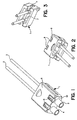
- Figur 1, 2 und 3 zeigen, aus jeweils unterschiedlicher Perspektive, eine Ausführungsform des Steckverbindergehäuses als Buchsenstecker,
- Figur 4, 5 und 6 zeigen, ebenfalls aus jeweils unterschiedlicher Perspektive, eine Ausführungsform des Steckverbindergehäuses als zum Buchsenstecker gemäß Figur 1, 2 und 3 komplementärer Stiftstecker.
- In Figur 1, 2 und 3 ist ein aus Kunststoff bestehendes Buchsengehäuse 1 gezeigt, in welchem die mit einer Ummantelung aus Kunststoff versehenen Lichtwellenleiter 2 und 3 fixiert sind. An das Buchsengehäuse 1 sind an seiner Stirnseite 10 zylindrische Buchsen 4 und 5 angeformt, während an der Stirnseite 11 des Stiftgehäuses 6 gemäß Figur 4, 5 und 6 eine komplementäre Stiftgeometrie ausgebildet ist. Im Buchsengehäuse 1 sind, ebenso wie im Stiftgehäuse 6, Ausnehmungen 7 vorhandenen, die zur Materialentnahme, d. h. zur Vermeidung von Masseanhäufungen im Gehäuse 1 bzw. 6 dienen. Diese Ausnehmungen 7, die je nach Anwendung stark variieren können, sind vor allem in den Figuren 2, 3, und 5 erkennbar.
- Weiter sind in den Figuren 1, 2, 4 und 5 Aussparungen 8 in der Außenwand 9 der Gehäuse 1 bzw. 6 erkennbar. Die Lichtwellenleiter 2 und 3 werden bei der Konfektionierung beispielsweise des Buchsengehäuses 1 in das einteilige Buchsengehäuse 1 so eingeführt, dass die Enden der Plastikfasern 2 und 3 im Wesentlichen plan an der dort offenen Stirnseite 10 (in der Mitte der zylindrischen Buchsen 4 bzw. 5) liegen.
- Zum Verschweißen kann beispielsweise Laserlicht mit einer Wellenlänge im so genannten nahen Infrarotbereich (800 bis 810 nm) eingesetzt werden. Für eine zugfeste Fixierung ist es ausreichend, für jeden Lichtwellenleiter 2 und 3 einen leicht ovalen, ca. drei bis vier Millimeter langen Schweißpunkt auf den Mantel des Lichtwellenleiters 2 bzw. 3 zu setzen. Der Laser ist so eingestellt, dass, bei einer gegebenen Transmission, eine Schweißung noch durch eine Wandstärke von beispielsweise zwei bis drei Millimetern hindurch gelingt. Diese Schweiß-Parameter werden nicht abhängig vom Anwendungs-Einzelfall jeweils neu eingestellt, sondern es wird die Tiefe der Aussparung 8 vorteilhaft so bemessen, dass eine definierte Wanddicke zur Schweißstelle hin von, in genannten Beispiel, zwei bis drei Millimetern verbleibt.
- Die Transmission durch das Buchsengehäuse 1 bzw. das Stiftgehäuse 6 hängt - abgesehen von der Wanddicke - vor allem vom Kunststoffmaterial und von etwaigen Additiven, wie Farbstoffen oder Füllstoffen, ab. Inzwischen sind Farbstoffe verfügbar, die im Wellenlängenbereich sichtbaren Lichts schwarz erscheinen, jedoch eine hohe Durchlässigkeit für Licht aus dem nahen Infrarot zeigen. Schwarze Steckverbindergehäuse sind erfindungsgemäß also ohne weiteres möglich.
- Die bisherigen Steckverbindergehäuse wurden insbesondere bei Anwendungen, die eine hohe Datenrate erfordern, beispielsweise im Kfz-, im EDV-Bereich oder in der Unterhaltungselektronik, mit einem äußeren Blechteil zur EMV-Abschirmung versehen. Diese konventionelle Ausgestaltung der Abschirmung ist - gegebenenfalls nach dem Schweißvorgang - auch bei dem erfindungsgemäßen Steckverbindergehäuse möglich. Das Steckverbindergehäuse kann jedoch vorteilhaft auch im so genannten 2-Komponenten-Spritzgießen hergestellt sein. Das Steckverbindergehäuse besteht dann einerseits aus einem laserverschweißbaren, für das verwendete Laserlicht transparentem Material und, andererseits, aus einem Material mit einer anderen technischen Eigenschaft, zum Beispiel EMV-Abschirmung.
- Eine weitere Möglichkeit besteht darin, das gesamte Steckverbindergehäuse aus einem einzigen, für das zum Schweißen verwendete Laserlicht transparentem Material spritzzugießen, die Außenwand 9 dann jedoch selektiv zu metallisieren.
- Eine vorteilhafte Variante besteht darin, das Steckverbindergehäuse aus einem für das zum Schweißen verwendete Laserlicht transparenten, für das von einer Sendediode emittierte Licht (zum Beispiel rot, 650 nm) aber undurchlässigen Material herzustellen. Dieses Steckverbindergehäuse ist laserverschweißbar, jedoch wird gleichzeitig optisches Übersprechen der Sender- bzw. Empfängerelemente verhindert.
-
- 1
- Buchsengehäuse
- 2
- Lichtwellenleiter
- 3
- Lichtwellenleiter
- 4
- Buchse
- 5
- Buchse
- 6
- Stiftgehäuse
- 7
- Ausnehmungen in 1 bzw. 6
- 8
- Aussparungen in 9
- 9
- Außenwand von 1 bzw. 6
- 10
- Stirnseite von 1
- 11
- Stirnseite von 6
Claims (7)
- Optische Steckverbindung mit einem Steckverbinder (1, 6), dessen Steckverbindergehäuse (1, 6) einen Lichtwellenleiter (2, 3) ohne eine diesen umgebende Ferrule aufnimmt, wobeidas Steckverbindergehäuse (1, 6) aus Kunststoff hergestellt ist und in dem mindestens ein Lichtwellenleiter (2, 3) ortsfest positioniert und mechanisch fixiert ist, dadurch gekennzeichnet, dassdas Steckverbindergehäuse (1, 6) unmittelbar an einen Mantel des Lichtwellenleiters (2, 3) geschweißt ist, wobei das Steckverbindergehäuse (1, 6) transparenter als der Mantel ausgebildet ist und mittels einer Laserschweißung im Durchstrahlverfahren an den Lichtwellenleiter (2, 3) befestigt ist.
- Optische Steckverbindung nach Anspruch 1, dadurch gekennzeichnet, dass die Laserschweißung zumindest bereichsweise im Berührungsbereich zwischen Steckverbindergehäuse (1, 6) und Lichtwellenleiter (2, 3) erfolgt.
- Optische Steckverbindung nach Anspruch 2, dadurch gekennzeichnet, dass in einer Außenwand (9) des Steckverbindergehäuses (1, 6) mindestens eine die Außenwand (9) bis in eine vorgegebene Tiefe öffnende Aussparung (8) vorgesehen ist, so dass ein die Laserschweißung herstellender Laserstrahl durch die dort mit definierter Wanddicke verbliebene Außenwand (9) hindurch Zugang zu dem dahinter liegenden Schweißbereich hat.
- Optische Steckverbindung nach einem der Ansprüche 1 bis 3, dadurch gekennzeichnet, dass das Steckverbindergehäuse (1, 6) für das zum Schweißen verwendete Laserlicht wenigstens teilweise transparent und für das von den Lichtwellenleiter-Komponenten verwendete Licht undurchlässig ist.
- Optische Steckverbindung nach einem der Ansprüche 1 bis 4, dadurch gekennzeichnet, dass das Steckverbindergehäuse (1, 6) mittels 2-Komponenten-Spritzgießen hergestellt ist, wobei als erste Spritzkomponente ein im Durchstrahlverfahren laserschweißbares Material und als zweite Spritzkomponente ein nicht-laserschweißbares Material vorgesehen ist.
- Optische Steckverbindung nach einem der Ansprüche 1 bis 5, dadurch gekennzeichnet, dass an der Außenwand (9) des Steckverbindergehäuses (1, 6) entweder eine selektive, auf Bereiche ohne dahinter liegenden Schweißbereich beschränkte Metallisierung, oder ein Schirmblech vorgesehen ist.
- Optische Steckverbindung nach Anspruch 5, dadurch gekennzeichnet, dass das nicht-laserschweißbare Material auf eine EMV-Abschirmung hin optimiert ist.
Priority Applications (1)
| Application Number | Priority Date | Filing Date | Title |
|---|---|---|---|
| EP03015062A EP1380867B1 (de) | 2002-07-13 | 2003-07-03 | Steckverbindergehäuse für Lichtwellenleiter |
Applications Claiming Priority (3)
| Application Number | Priority Date | Filing Date | Title |
|---|---|---|---|
| EP02015731 | 2002-07-13 | ||
| EP02015731 | 2002-07-13 | ||
| EP03015062A EP1380867B1 (de) | 2002-07-13 | 2003-07-03 | Steckverbindergehäuse für Lichtwellenleiter |
Publications (3)
| Publication Number | Publication Date |
|---|---|
| EP1380867A2 EP1380867A2 (de) | 2004-01-14 |
| EP1380867A3 EP1380867A3 (de) | 2004-11-17 |
| EP1380867B1 true EP1380867B1 (de) | 2007-09-12 |
Family
ID=29737936
Family Applications (1)
| Application Number | Title | Priority Date | Filing Date |
|---|---|---|---|
| EP03015062A Expired - Lifetime EP1380867B1 (de) | 2002-07-13 | 2003-07-03 | Steckverbindergehäuse für Lichtwellenleiter |
Country Status (1)
| Country | Link |
|---|---|
| EP (1) | EP1380867B1 (de) |
Families Citing this family (2)
| Publication number | Priority date | Publication date | Assignee | Title |
|---|---|---|---|---|
| DE102011003686A1 (de) * | 2011-02-07 | 2012-08-09 | Trumpf Laser- Und Systemtechnik Gmbh | Laserbearbeitungsvorrichtung |
| DE102011016709A1 (de) * | 2011-04-11 | 2012-10-11 | Tyco Electronics Amp Gmbh | Kupplungselement für Lichtwellenleiter, Steckverbinder und Herstellungsverfahren |
Family Cites Families (7)
| Publication number | Priority date | Publication date | Assignee | Title |
|---|---|---|---|---|
| US4859827A (en) * | 1988-10-17 | 1989-08-22 | American Telephone And Telegraph Company | Method for welding relatively small parts |
| DE19822990A1 (de) * | 1998-05-22 | 1999-11-25 | Amphenol Tuchel Elect | Steckverbinder |
| US6206582B1 (en) * | 1999-01-22 | 2001-03-27 | Stratos Lightwave, Inc. | EMI reduction for optical subassembly |
| DE19919428C2 (de) * | 1999-04-28 | 2001-12-06 | Tyco Electronics Logistics Ag | Kunststoff-Ferrule für einen Lichtwellenleiter und Verfahren zum Befestigen einer Ferrule an einem Lichtwellenleiter |
| AU4529600A (en) * | 1999-04-30 | 2000-11-17 | Powerlasers Ltd. | Method of clamping thermoplastic pieces and heat control for laser welding |
| CZ20023726A3 (cs) * | 2000-05-13 | 2003-05-14 | Tyco Electronics Amp Gmbh | Polohovací zařízení sloužící k přivaření světelného vlnovodu laserem k ochrannému kroužku ze syntetického materiálu |
| JP4443750B2 (ja) * | 2000-09-29 | 2010-03-31 | 古河電気工業株式会社 | 光ファイバの固定構造 |
-
2003
- 2003-07-03 EP EP03015062A patent/EP1380867B1/de not_active Expired - Lifetime
Also Published As
| Publication number | Publication date |
|---|---|
| EP1380867A3 (de) | 2004-11-17 |
| EP1380867A2 (de) | 2004-01-14 |
Similar Documents
| Publication | Publication Date | Title |
|---|---|---|
| EP2003477B1 (de) | Elektro-optische Hybrid-Steckverbindung zur Übertragung von hohen optischen Leistungen und elektrischen Signalen | |
| EP1180248B1 (de) | Verfahren zum befestigen einer ferrule an einem lichtwellenleiter | |
| EP0238977B1 (de) | Sende- und Empfangsmodul für ein bidirektionales Kommunikationsnetz, insbesondere ein Breitband-ISDN | |
| DE102007054747B4 (de) | Lichtleitkabel-Kontakt, Lichtleitkabel-Verbinder sowie konfektioniertes Lichtleitkabel | |
| EP2962142B1 (de) | Optisches modul für modular aufgebaute industriesteckverbinder | |
| DE69620130T2 (de) | Optisches Sender-Empfänger-Modul | |
| DE112007002109T5 (de) | Wellenleiter für Kunststoffschweißen unter Verwendung einer inkohärenten Infrarot-Lichtquelle | |
| CH697509B1 (de) | Laserschweisseinrichtung, bestehend aus einem Lichtleiter oder einem Lichtwellenleiter mit einem optischen Trichter. | |
| DE68914321T2 (de) | Lichtabschwächer und Verfahren zu seiner Herstellung. | |
| DE112008001167T5 (de) | Infrarot-Kunststoffschweißen unter Rückführung nicht absorbierten Infrarot-Laserlichts zur Erhöhung der Absorption von Infrarot-Laserlicht | |
| DE4341417C2 (de) | Lichtwellenleiter-Endabschlußvorrichtung | |
| DE4219901A1 (de) | Lichtwellenleiter-Abschlußhülse | |
| DE10033785C2 (de) | Vorrichtung zum Einkoppeln von Laserstrahlen in eine Lichtleitfaser | |
| DE10127331B4 (de) | Verfahren zum Verbinden mindestens einer optischen Faser mit einer GRIN-Linse und Filtermodul | |
| EP1380867A2 (de) | Steckverbindergehäuse für Lichtwellenleiter | |
| DE102008030187B4 (de) | Vorrichtung zur Übertragung von optischen Signalen zwischen relativ zueinander drehbaren Baugruppen (Drehübertrager) | |
| DE2748503A1 (de) | Optisches verbindungselement fuer lichtleitfasern | |
| EP2018583B1 (de) | Steckverbinder mit vorrichtung zur kompensation von längenausdehnungen eines lichtwellenleiters | |
| DE3407413C2 (de) | ||
| EP0522305B1 (de) | Verfahren zur Herstellung eines Verbindungselements für aus Kunststoff bestehende, lichtleitende Fasern | |
| DE19858474B4 (de) | Verfahren zum Herstellen von Stirnflächen an Lichtwellenleitern aus optischen Fasern aus Kunststoff (POF) und Vorrichtung zur Durchführung des Verfahrens | |
| DE2835582A1 (de) | Verbindungselement fuer lichtleiterkabel sowie vorrichtung und verfahren zu seiner anbringung | |
| DE10258481B4 (de) | Fiberoptisches Beleuchtungssystem und Verfahren zu dessen Herstellung | |
| DE19840439C2 (de) | Steckvorrichtung für einen Lichtwellenleiter und Verfahren zu deren Herstellung | |
| EP1022593A1 (de) | Verfahren zur Konfektionierung eines Lichtleiters |
Legal Events
| Date | Code | Title | Description |
|---|---|---|---|
| PUAI | Public reference made under article 153(3) epc to a published international application that has entered the european phase |
Free format text: ORIGINAL CODE: 0009012 |
|
| AK | Designated contracting states |
Kind code of ref document: A2 Designated state(s): AT BE BG CH CY CZ DE DK EE ES FI FR GB GR HU IE IT LI LU MC NL PT RO SE SI SK TR |
|
| AX | Request for extension of the european patent |
Extension state: AL LT LV MK |
|
| PUAL | Search report despatched |
Free format text: ORIGINAL CODE: 0009013 |
|
| AK | Designated contracting states |
Kind code of ref document: A3 Designated state(s): AT BE BG CH CY CZ DE DK EE ES FI FR GB GR HU IE IT LI LU MC NL PT RO SE SI SK TR |
|
| AX | Request for extension of the european patent |
Extension state: AL LT LV MK |
|
| RIC1 | Information provided on ipc code assigned before grant |
Ipc: 7B 23K 26/00 B Ipc: 7G 02B 6/36 B Ipc: 7G 02B 6/38 A |
|
| 17P | Request for examination filed |
Effective date: 20050509 |
|
| AKX | Designation fees paid |
Designated state(s): AT BE BG CH CY CZ DE DK EE ES FI FR GB GR HU IE IT LI LU MC NL PT RO SE SI SK TR |
|
| GRAP | Despatch of communication of intention to grant a patent |
Free format text: ORIGINAL CODE: EPIDOSNIGR1 |
|
| GRAS | Grant fee paid |
Free format text: ORIGINAL CODE: EPIDOSNIGR3 |
|
| GRAA | (expected) grant |
Free format text: ORIGINAL CODE: 0009210 |
|
| AK | Designated contracting states |
Kind code of ref document: B1 Designated state(s): AT BE BG CH CY CZ DE DK EE ES FI FR GB GR HU IE IT LI LU MC NL PT RO SE SI SK TR |
|
| REG | Reference to a national code |
Ref country code: GB Ref legal event code: FG4D Free format text: NOT ENGLISH |
|
| REG | Reference to a national code |
Ref country code: CH Ref legal event code: EP |
|
| REF | Corresponds to: |
Ref document number: 50308153 Country of ref document: DE Date of ref document: 20071025 Kind code of ref document: P |
|
| REG | Reference to a national code |
Ref country code: IE Ref legal event code: FG4D Free format text: LANGUAGE OF EP DOCUMENT: GERMAN |
|
| PG25 | Lapsed in a contracting state [announced via postgrant information from national office to epo] |
Ref country code: FI Free format text: LAPSE BECAUSE OF FAILURE TO SUBMIT A TRANSLATION OF THE DESCRIPTION OR TO PAY THE FEE WITHIN THE PRESCRIBED TIME-LIMIT Effective date: 20070912 |
|
| NLV1 | Nl: lapsed or annulled due to failure to fulfill the requirements of art. 29p and 29m of the patents act | ||
| GBV | Gb: ep patent (uk) treated as always having been void in accordance with gb section 77(7)/1977 [no translation filed] | ||
| PG25 | Lapsed in a contracting state [announced via postgrant information from national office to epo] |
Ref country code: GR Free format text: LAPSE BECAUSE OF FAILURE TO SUBMIT A TRANSLATION OF THE DESCRIPTION OR TO PAY THE FEE WITHIN THE PRESCRIBED TIME-LIMIT Effective date: 20071213 Ref country code: ES Free format text: LAPSE BECAUSE OF FAILURE TO SUBMIT A TRANSLATION OF THE DESCRIPTION OR TO PAY THE FEE WITHIN THE PRESCRIBED TIME-LIMIT Effective date: 20071223 Ref country code: NL Free format text: LAPSE BECAUSE OF FAILURE TO SUBMIT A TRANSLATION OF THE DESCRIPTION OR TO PAY THE FEE WITHIN THE PRESCRIBED TIME-LIMIT Effective date: 20070912 |
|
| REG | Reference to a national code |
Ref country code: IE Ref legal event code: FD4D |
|
| ET | Fr: translation filed | ||
| PG25 | Lapsed in a contracting state [announced via postgrant information from national office to epo] |
Ref country code: GB Free format text: LAPSE BECAUSE OF FAILURE TO SUBMIT A TRANSLATION OF THE DESCRIPTION OR TO PAY THE FEE WITHIN THE PRESCRIBED TIME-LIMIT Effective date: 20070912 Ref country code: CZ Free format text: LAPSE BECAUSE OF FAILURE TO SUBMIT A TRANSLATION OF THE DESCRIPTION OR TO PAY THE FEE WITHIN THE PRESCRIBED TIME-LIMIT Effective date: 20070912 Ref country code: PT Free format text: LAPSE BECAUSE OF FAILURE TO SUBMIT A TRANSLATION OF THE DESCRIPTION OR TO PAY THE FEE WITHIN THE PRESCRIBED TIME-LIMIT Effective date: 20080212 Ref country code: SK Free format text: LAPSE BECAUSE OF FAILURE TO SUBMIT A TRANSLATION OF THE DESCRIPTION OR TO PAY THE FEE WITHIN THE PRESCRIBED TIME-LIMIT Effective date: 20070912 |
|
| PG25 | Lapsed in a contracting state [announced via postgrant information from national office to epo] |
Ref country code: SE Free format text: LAPSE BECAUSE OF FAILURE TO SUBMIT A TRANSLATION OF THE DESCRIPTION OR TO PAY THE FEE WITHIN THE PRESCRIBED TIME-LIMIT Effective date: 20071212 Ref country code: RO Free format text: LAPSE BECAUSE OF FAILURE TO SUBMIT A TRANSLATION OF THE DESCRIPTION OR TO PAY THE FEE WITHIN THE PRESCRIBED TIME-LIMIT Effective date: 20070912 |
|
| PLBE | No opposition filed within time limit |
Free format text: ORIGINAL CODE: 0009261 |
|
| STAA | Information on the status of an ep patent application or granted ep patent |
Free format text: STATUS: NO OPPOSITION FILED WITHIN TIME LIMIT |
|
| PG25 | Lapsed in a contracting state [announced via postgrant information from national office to epo] |
Ref country code: DK Free format text: LAPSE BECAUSE OF FAILURE TO SUBMIT A TRANSLATION OF THE DESCRIPTION OR TO PAY THE FEE WITHIN THE PRESCRIBED TIME-LIMIT Effective date: 20070912 |
|
| 26N | No opposition filed |
Effective date: 20080613 |
|
| PG25 | Lapsed in a contracting state [announced via postgrant information from national office to epo] |
Ref country code: IE Free format text: LAPSE BECAUSE OF FAILURE TO SUBMIT A TRANSLATION OF THE DESCRIPTION OR TO PAY THE FEE WITHIN THE PRESCRIBED TIME-LIMIT Effective date: 20070912 |
|
| REG | Reference to a national code |
Ref country code: CH Ref legal event code: PL |
|
| PG25 | Lapsed in a contracting state [announced via postgrant information from national office to epo] |
Ref country code: MC Free format text: LAPSE BECAUSE OF NON-PAYMENT OF DUE FEES Effective date: 20080731 |
|
| PG25 | Lapsed in a contracting state [announced via postgrant information from national office to epo] |
Ref country code: EE Free format text: LAPSE BECAUSE OF FAILURE TO SUBMIT A TRANSLATION OF THE DESCRIPTION OR TO PAY THE FEE WITHIN THE PRESCRIBED TIME-LIMIT Effective date: 20070912 |
|
| PG25 | Lapsed in a contracting state [announced via postgrant information from national office to epo] |
Ref country code: CH Free format text: LAPSE BECAUSE OF NON-PAYMENT OF DUE FEES Effective date: 20080731 Ref country code: LI Free format text: LAPSE BECAUSE OF NON-PAYMENT OF DUE FEES Effective date: 20080731 Ref country code: SI Free format text: LAPSE BECAUSE OF FAILURE TO SUBMIT A TRANSLATION OF THE DESCRIPTION OR TO PAY THE FEE WITHIN THE PRESCRIBED TIME-LIMIT Effective date: 20070912 |
|
| PG25 | Lapsed in a contracting state [announced via postgrant information from national office to epo] |
Ref country code: CY Free format text: LAPSE BECAUSE OF FAILURE TO SUBMIT A TRANSLATION OF THE DESCRIPTION OR TO PAY THE FEE WITHIN THE PRESCRIBED TIME-LIMIT Effective date: 20070912 |
|
| PG25 | Lapsed in a contracting state [announced via postgrant information from national office to epo] |
Ref country code: BG Free format text: LAPSE BECAUSE OF FAILURE TO SUBMIT A TRANSLATION OF THE DESCRIPTION OR TO PAY THE FEE WITHIN THE PRESCRIBED TIME-LIMIT Effective date: 20071212 |
|
| PG25 | Lapsed in a contracting state [announced via postgrant information from national office to epo] |
Ref country code: AT Free format text: LAPSE BECAUSE OF NON-PAYMENT OF DUE FEES Effective date: 20080703 |
|
| PG25 | Lapsed in a contracting state [announced via postgrant information from national office to epo] |
Ref country code: LU Free format text: LAPSE BECAUSE OF NON-PAYMENT OF DUE FEES Effective date: 20080703 Ref country code: HU Free format text: LAPSE BECAUSE OF FAILURE TO SUBMIT A TRANSLATION OF THE DESCRIPTION OR TO PAY THE FEE WITHIN THE PRESCRIBED TIME-LIMIT Effective date: 20080313 Ref country code: BE Free format text: LAPSE BECAUSE OF NON-PAYMENT OF DUE FEES Effective date: 20080731 |
|
| PG25 | Lapsed in a contracting state [announced via postgrant information from national office to epo] |
Ref country code: TR Free format text: LAPSE BECAUSE OF FAILURE TO SUBMIT A TRANSLATION OF THE DESCRIPTION OR TO PAY THE FEE WITHIN THE PRESCRIBED TIME-LIMIT Effective date: 20070912 |
|
| REG | Reference to a national code |
Ref country code: FR Ref legal event code: PLFP Year of fee payment: 13 |
|
| REG | Reference to a national code |
Ref country code: DE Ref legal event code: R082 Ref document number: 50308153 Country of ref document: DE Representative=s name: WILHELM & BECK, DE Ref country code: DE Ref legal event code: R081 Ref document number: 50308153 Country of ref document: DE Owner name: TE CONNECTIVITY GERMANY GMBH, DE Free format text: FORMER OWNER: TYCO ELECTRONICS AMP GMBH, 64625 BENSHEIM, DE |
|
| REG | Reference to a national code |
Ref country code: FR Ref legal event code: CD Owner name: TE CONNECTIVITY GERMANY GMBH Effective date: 20151027 |
|
| REG | Reference to a national code |
Ref country code: FR Ref legal event code: PLFP Year of fee payment: 14 |
|
| REG | Reference to a national code |
Ref country code: FR Ref legal event code: PLFP Year of fee payment: 15 |
|
| REG | Reference to a national code |
Ref country code: FR Ref legal event code: PLFP Year of fee payment: 16 |
|
| PGFP | Annual fee paid to national office [announced via postgrant information from national office to epo] |
Ref country code: FR Payment date: 20180612 Year of fee payment: 16 |
|
| PGFP | Annual fee paid to national office [announced via postgrant information from national office to epo] |
Ref country code: IT Payment date: 20180713 Year of fee payment: 16 Ref country code: DE Payment date: 20180619 Year of fee payment: 16 |
|
| REG | Reference to a national code |
Ref country code: DE Ref legal event code: R119 Ref document number: 50308153 Country of ref document: DE |
|
| PG25 | Lapsed in a contracting state [announced via postgrant information from national office to epo] |
Ref country code: DE Free format text: LAPSE BECAUSE OF NON-PAYMENT OF DUE FEES Effective date: 20200201 |
|
| PG25 | Lapsed in a contracting state [announced via postgrant information from national office to epo] |
Ref country code: FR Free format text: LAPSE BECAUSE OF NON-PAYMENT OF DUE FEES Effective date: 20190731 |
|
| PG25 | Lapsed in a contracting state [announced via postgrant information from national office to epo] |
Ref country code: IT Free format text: LAPSE BECAUSE OF NON-PAYMENT OF DUE FEES Effective date: 20190703 |