EP1378913A1 - Spannungsverstärker und Speichersystem - Google Patents
Spannungsverstärker und Speichersystem Download PDFInfo
- Publication number
- EP1378913A1 EP1378913A1 EP03425442A EP03425442A EP1378913A1 EP 1378913 A1 EP1378913 A1 EP 1378913A1 EP 03425442 A EP03425442 A EP 03425442A EP 03425442 A EP03425442 A EP 03425442A EP 1378913 A1 EP1378913 A1 EP 1378913A1
- Authority
- EP
- European Patent Office
- Prior art keywords
- voltage
- terminal
- stand
- capacitor
- signal
- Prior art date
- Legal status (The legal status is an assumption and is not a legal conclusion. Google has not performed a legal analysis and makes no representation as to the accuracy of the status listed.)
- Granted
Links
Images


Classifications
-
- G—PHYSICS
- G11—INFORMATION STORAGE
- G11C—STATIC STORES
- G11C16/00—Erasable programmable read-only memories
- G11C16/02—Erasable programmable read-only memories electrically programmable
- G11C16/06—Auxiliary circuits, e.g. for writing into memory
- G11C16/10—Programming or data input circuits
- G11C16/12—Programming voltage switching circuits
-
- G—PHYSICS
- G11—INFORMATION STORAGE
- G11C—STATIC STORES
- G11C5/00—Details of stores covered by group G11C11/00
- G11C5/14—Power supply arrangements, e.g. power down, chip selection or deselection, layout of wirings or power grids, or multiple supply levels
- G11C5/145—Applications of charge pumps; Boosted voltage circuits; Clamp circuits therefor
-
- G—PHYSICS
- G11—INFORMATION STORAGE
- G11C—STATIC STORES
- G11C8/00—Arrangements for selecting an address in a digital store
- G11C8/08—Word line control circuits, e.g. drivers, boosters, pull-up circuits, pull-down circuits, precharging circuits, for word lines
-
- G—PHYSICS
- G11—INFORMATION STORAGE
- G11C—STATIC STORES
- G11C2207/00—Indexing scheme relating to arrangements for writing information into, or reading information out from, a digital store
- G11C2207/22—Control and timing of internal memory operations
- G11C2207/2227—Standby or low power modes
Definitions
- the following invention relates to a voltage booster device of the type used in non-volatile memories.
- the voltage booster devices commonly used include boosters based on the charge pump principle.
- a charge pump booster behaves as a voltage generator with non-null output resistance, for which the current that can be requested of it is inversely proportionate to the voltage that it must supply.
- this type of booster does not make it possible to supply voltage with the necessary precision and, therefore, an adjustment circuit of the booster output voltage is conveniently used.
- the voltage booster device With the aim of reducing consumption, when operations are not being performed on the non-volatile memory the voltage booster device is deactivated or rather, it is taken to a wait or stand-by status.
- the document EP-A-1113450 describes a voltage booster device including, in addition to booster and a regulator, also a stand-by booster device to operate on the stand-by input.
- a stand-by booster device At the stand-by input, an output node of the booster and an output node of the voltage regulator are connected to one another and with an output terminal of the stand-by voltage booster device.
- the stand-by booster device is used to supply to such nodes a voltage necessary to compensate the discharge due to junction leakage currents (inverse saturation currents) of the transistors connected to it. According to the abovementioned document, thanks to the action of this stand-by booster device it is possible, on exiting stand-by, to reach the reading voltage required quickly and accurately.
- the aim of the present invention is to provide a voltage booster device that presents superior performances than those of the conventional devices described above.
- the aim of the present invention is achieved by a voltage booster device as defined in the annexed claims 1 to 21.
- object of the present invention is a memory system including a voltage booster device as defined in the annexed claim 22.
- Figure 1 illustrates a non-volatile memory system 1 comprising a matrix or a memory array 2, a voltage booster device 3 including a reading voltage booster stage 4, a wait or stand-by voltage booster stage (STAND-BY) 5 and circuital means of discharge management 100.
- a voltage booster device 3 including a reading voltage booster stage 4, a wait or stand-by voltage booster stage (STAND-BY) 5 and circuital means of discharge management 100.
- STAND-BY wait or stand-by voltage booster stage
- the memory array 2 is, for example, of the low supply voltage (for example equal to 3V) multi-level Flash type and comprises a plurality of memory cells 6 organised in rows and columns.
- the memory cells 6 belonging to the same row have their gate terminals connected to a row or word line 7.
- a row decoder 8 for example, of the conventional type, selectively connects one of the memory array 2 word lines 7 to an output terminal 10 of the voltage booster device 3.
- the row decoder 8 has a parasitic capacity represented in figure 1 by a decodification capacitor 11 connected between said output terminal 10 and the ground.
- the reading voltage booster stage 4 is, for example, of a conventional type and comprises a reading positive charge pump booster 12 having an output terminal in order to make available a reading voltage VR connected by a first commutator 13 to a first node 15. Said reading voltage VR is suitably higher in module in relation to a supply voltage VDD of the memory system 1 and the booster 12.
- the first branch line 15 can be selectively (or rather reversibly) connected to a first terminal of a filter capacitor 16 with capacity C 16 having a second terminal connected to the earth.
- the filter capacitor 16 has a function of filtering undesired components from the voltage at the first node 15 due to transients that occur following the switching on or off of the booster 12.
- the first node 15 is connected by a conduction line 15' to a reading voltage regulator input 17 provided with an output terminal in order to supply a regulated reading voltage VRR.
- the reading voltage regulator output terminal 17 is selectively connectable to the output terminal 10 of the voltage booster device 3 by a second commutator 18.
- the memory system 1 comprises a control unit (C.U.) 20 in order to generate a wait or stand-by signal SB and a timing signal CK.
- the stand-by SB signal for example, being a signal destined to assume two logic levels.
- the reading voltage booster stage 4 is such as to supply the regulated reading voltage VRR with a value suited to the reading of the memory matrix 2 when it is selected.
- this reading voltage booster stage is destined to be put in a stand-by status, or rather to be deactivated, by the stand-by signal SB (for example, with a high logic level) and to be activated to function when the memory matrix 2 is selected (for example, the SB signal assumes the low logic level).
- SB stand-by signal
- the stand-by voltage booster stage 5 is created in the same way as described in the abovementioned patent application EP-A-1113450 with reference to the stage indicated with the number 5.
- the stand-by voltage booster stage 5 can be activated and deactivated to/from functioning on the basis of the stand-by signal SB.
- Such stand-by voltage booster stage 5 has the function of maintaining, during the stand-by status, the output terminal 10 (together with the node 15) charged to a desired voltage value in order to enable the swift reading in output of a stand-by status and at the same time limiting consumption to that strictly necessary.
- the stand-by voltage booster stage 5 makes it possible to compensate the reduction of the electric potential of the output terminal 10 and the first node 15 that occurs in the stand-by status and due to leakage currents, or rather to the inverse junction saturation current pn or np of MOSFET transistors used in the memory system.
- the stand-by voltage booster stage 5 For the charging to a desired voltage of the output terminal 10 such a stand-by voltage booster stage 5, makes available a charging signal STBYPMPOUT supplied to a second node 103.
- the stand-by voltage booster stage 5 comprises a voltage comparator, a phase generator, a positive charge pump booster and an optional auxiliary voltage regulator (not shown). A more detailed description of the stand-by voltage booster stage 5 is made in the document mentioned and is therefore not necessary in the present description.
- the discharge management circuit 100 comprises a detection and discharge stage DT-DSC having an input terminal connected to the first node 15.
- the discharge management circuit 100 is also provided with means of commutation including a first high voltage switch or commutator 101 destined to connect/disconnect the first node 15 to/from the second node 103 in turn connected to a second high voltage switch 102.
- the second high voltage switch 102 is such to connect/disconnect the second node 103, also connected to the output of the stand-by voltage booster stage 5, at the output terminal 10.
- the discharge management circuit 100 makes it possible, during memory stand-by 2, to discharge the first node 15 and, therefore, the filter capacitor 16 when the electrical potential of said first node 15 is higher in module than a desired value V-SB.
- the desired value V-SB is a value such as assures that on exiting stand-by the voltage present on the output terminal 10 is suitable for performing a specific operation such as, in particular, the reading of a memory cell (for example, the voltage at the output terminal 10 is of 6V).
- the discharge management circuit 100 makes it possible to discharge the first capacitor 16 in order to avoid perturbations of the output terminal 10 due to interactions between the first 16 and second 11 capacitor that can be checked when the first node 15 and the output terminal 10 are connected.
- the detection and discharge circuit DT-DSC makes it possible to generate a first piloting signal PMPCONHV_N of the first high voltage commutator 101 and a second piloting signal REGCONHV_N of the second high voltage commutator 102.
- Figure 2 schematically illustrates a preferred embodiment of the detection and discharge circuit, comprising a voltage divider 105 and a discharge device 106 (DISCHARGE).
- the voltage divider 104 includes, for example, a number N2 of diodes 107 connected in series between the first node 15 and the ground in order to divide the output voltage from the positive charge pump booster 12 thus generating an output voltage V-DIV to be supplied to a non-inverting terminal of the voltage comparator 105.
- the voltage comparator 105 supplied by a voltage VDD, is such to compare the voltage V -DIV withdrawn by the voltage divider 104 with a reference voltage VREF supplied to an inverting terminal and generate a discharge-command signal PMPDISCH in output. Moreover, the voltage comparator 105 is activated/deactivated by a logic activation signal PMPDISCHEN.
- the activation signal PMPDISCHEN makes active the voltage comparator 105 (for example, by assuming a high logic level), when entry into stand-by occurs and deactivates it, thus reducing supply consumption, when the discharge device 106 has performed its discharge function or, if such a discharge function has not occurred completely, when the memory system 1 exits stand-by.
- the discharge device 106 piloted by the command-discharge signal PMPDISCH, makes it possible to discharge to earth the voltage of the first node 15 until voltage is equal to the value V-SB.
- the discharge device is created by a MOSFET (Metal-Oxide-Semiconductor-Field-Effect-Transistor), in particular, at channel N, and represented in the same figure 2 by the discharge transistor 108.
- MOSFET Metal-Oxide-Semiconductor-Field-Effect-Transistor
- Such a transistor 108 presents the gate terminal connected to the output of the voltage comparator 105, in such a way as to be activated and deactivated according to the discharge-command signal PMPDISCH, and the remaining terminals connected to the first node 15 and to the earth.
- the discharge phase such a transistor 108 is crossed by Idisch discharge current.
- the discharge takes place when the command-discharge signal PMPDISCH assumes a high logical level. It should be observed that, advantageously, the discharge caused is sufficiently fast as to not maintain the voltage comparator 105 in function too long and, at the same time, it is sufficiently slow to consent an efficient control by the voltage comparator 105.
- the voltage divider 104 can be created by a cascade of N2 P-type MOS transistors connected to a diode.
- such a voltage divider 104 is substantially identical to the voltage divider used in the stand-by voltage booster stage 5 and described in the abovementioned state of the art document. In this way, mismatching problems between the detection at the first node 15 and that at the output terminal 10 performed by the stand-by voltage booster stage 5 are reduced.
- the detection and discharge circuit DT-DSC is also fitted with completed discharge signal LOWPMP generation stage 109 obtained starting from the command-discharge signal PMPDISCH.
- such a generation stage 109 can be created using a flip-flop, FF, for example a type d model, synchronised by the command-discharge signal PMPDISCH applied to a CP input and such as to enable the flip flop 109 in correspondence with the descent fronts.
- FF flip-flop
- PMPDISCH command-discharge signal
- the signal LOWPMP present on the output Q will assume the value VDD of the supply voltage applied at the input D each time a descent front of the command-discharge signal PMPDISCH is present.
- Flip-flop 109 reset occurs as a consequence to the exiting of stand-by status or rather, according to the example, when the stand-by signal SB assumes a low logic level.
- the detection and discharge circuit DT-DSC also comprises a voltage booster 110 (also indicated in figure 2 with ELEVATOR) destined to invert and raise the voltage of the completed discharge signal LOWPMP and the stand-by signal SB generating on corresponding outputs, the first piloting signal PMPCONHV_N of the first high voltage commutator 101 and the second piloting signal REGCONHV_N of the second high voltage commutator 102 respectively.
- a voltage booster 110 also indicated in figure 2 with ELEVATOR
- the detection and discharge circuit DT-DSC is also provided with a suitable logic network 111 (indicated in the figure with the caption LOG+DELAY) comprising, for example, an inverting element and, preferably also a delay element that assures a margin of safety in the times of the device 3.
- a suitable logic network 111 (indicated in the figure with the caption LOG+DELAY) comprising, for example, an inverting element and, preferably also a delay element that assures a margin of safety in the times of the device 3.
- the logic network 111 starting from the discharge completed signal LOWPMP is such to generate the activation signal PMPDISCHEN to send to the voltage comparator 105.
- control unit 20 assigns to the stand-by signal SB the high logic level.
- the first high voltage commutator 101 On entering the stand-by status, the first high voltage commutator 101 is kept open and the second high voltage commutator 102 is closed by the second piloting signal REGCONVH_N. In this way, during an initial phase, the output terminal 10 is connected to the stand-by voltage booster stage 5 whilst the first node 15, directly connected to the detection and discharge stage DT_DSC, is not connected with the stand-by voltage booster stage 5.
- the activation signal PMPDISCHEN is at a high logic level and such as to activate the operation of the voltage comparator 105.
- the voltage divider 104 withdraws the voltage present at the first node and sends the corresponding voltage V-DIV to the voltage comparator 105.
- the voltage comparator 105 If the voltage V-15 present at the first node 15 is higher than the preset value V-SB, and therefore the voltage V-DIV is higher than reference voltage VREF, the voltage comparator 105 generates the command-discharge signal PMPDISCH with a high logical level and sufficient to cause a discharge through the device 106.
- the level of the command-discharge signal PMPDISCH is such to take to conduction the transistor 108 which, by means of the Idisch current discharges towards earth part of the charge of the filter condenser 16.
- the command-discharge signal PMPDISCH reaches a logic level such as to interrupt the discharge of the first node 15.
- the command-discharge signal PMPDISCH is also sent to the flip-flop 109.
- the descent front of the command-discharge signal PMPDISCH applied to the flip-flop 109 causes the activation (high logic level) of the discharge completed signal LOWPMP.
- the network 111 takes the command-discharge activation signal PMPDISCHEN to a low logic level in order to deactivate the voltage comparator 105 from function.
- the deactivation of the voltage comparator 105 interrupts a further discharge of the node voltage 15 and, advantageously, prevents consumptions due to the voltage comparator itself.
- the booster stage 110 inverts and boosts in voltage the discharge completed signal LOWPMP in order that the signal PMPCONHV-N assumes an adequate voltage level to close the first high voltage switch 101 by connecting the first node 15 to the terminal 10 and, therefore, to the stand-by voltage booster stage 5.
- the stand-by voltage booster stage 5 will see to maintaining the voltage of the output terminal 10, connected to the first node 15 and to the two respective capacitors 11 and 16, at the value V-SB charging it with the voltage STBYPMPOUT supplied to the second node 103.
- the controlled discharge of the node 15 voltage and, therefore, of the filter capacitor 16, is particularly advantageous as is prevents the problems noted with conventional structures that provide, on entry to stand-by, an immediate connection, of the output node of the booster stage with the output terminal of the voltage regulator and, therefore, the connection of such common node with the stand-by voltage booster stage.
- structures having a similar function to that of the booster device described in the document EP-A-1113450 it has been noted that one can present a duration of the permanence in stand-by status such as to not permit that one reaches the exhaustion of a transient due to the coupling or sharing between the filter capacitor connected to the booster and the decodification capacitor connected to the voltage regulator. It should be noted how on entry to the stand-by status the filter capacitor 16 and the decodification capacitor 11 present voltages V-16 and V-11 respectively.
- Such a saturation status makes vain the control action exerted by the stand-by voltage booster stage 5 and, in some cases, can lead to incorrect cell reading.
- the voltage of the filter capacitor 16 is forced, on entering the stand-by status and before connecting the first node 15 to the output terminal 10, to assume the desired value V-SB without awaiting the exhaustion of the transient due to sharing with the decodification capacitor 11.
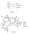
- Figure 4 illustrates a preferred embodiment of the voltage comparator 105.
- the voltage comparator is created in CMOS (Complementary Metal-Oxide-Semiconductor) technology and includes MOS transistors.
- CMOS Complementary Metal-Oxide-Semiconductor
- This voltage comparator 105 comprises a differential amplifier D-P including a pair of transistors (of type N) M1 and M2 and an active charge including a current mirror CM formed by two transistors (of type P) M3 and M4.
- transistors M1 and M2 of the differential amplifier D-P can be supplied the voltage V-DIV exiting from the voltage divider 104 and the reference voltage VREF respectively.
- the source terminals of the transistors M1 and M2 are both connected to the drain of a first activation/deactivation transistor (of type N) M6 destined to receive the activation signal of the voltage comparator PMPDISCHEN at its gate.
- the first activation/deactivation transistor is connected in cascade with a transistor M6 (of type N) connected to the earth and having the respective gate terminal destined to receive the reference voltage VREF that takes it to conduction.
- the source terminals of the transistors M3 and M4 forming the current mirror CM are connected to the supply voltage VDD. Between the terminal supplied by the voltage VDD and the common gate terminals of transistors M3 and M4 of the current mirror CM a second activation/deactivation transistor (of type P) M7 is interposed, to the gate of which the voltage comparator activation signal PMPDISCHEN is applied.
- the drain terminal of the transistor M1 of the differential amplifier D-P is connected to an output line L on which, when the voltage comparator is activated, a signal correlated to the difference in the output voltage of the voltage divider V-DIV and the reference voltage VREF is made available.
- a third activation/deactivation transistor (of type P) M8 supplied by the voltage VDD and such as to receive in entry the activation signal PMPDISCHEN is connected.
- the output line L is connected to an intermediate stage PP including a higher P-type transistor, M9, connected in cascade to a lower N-type transistor, M10, having a terminal connected to ground.
- the line L is connected to the gate of the upper transistor M9, and the lower transistor M10 receives at its gate the reference voltage VREF.
- a common node CN of the upper and lower transistors is connected at the input to a first inverter I1 in turn connected to a second inverter I2 on whose output a command-discharge signal PMPDISCH is made available.
- the third activation transistor M8 is activated to function in order to take the output line L to voltage VDD (high level) and deactivate the upper transistor M9.
- VDD high level
- the lower transistor M10 a voltage such that at the output of the second inverter 12 the command-discharge signal PMPDISCH assumes a low logic level, that does not consent the discharge to be made, is taken to the input of the first inverter I1.
- the voltage comparator 105 in an active state, when the voltage V-DIV in output from the voltage divider 104 is higher than the voltage VREF, on the output line L of the differential amplifier D-P a signal such as to deactivate the upper transistor M9 of the intermediate stage PP from functioning is present. In this way, a signal is taken to the input of the first inverter I1 such that on output from the second inverter 12, the command-discharge signal PMPDISCH will assume a high logic level, that makes it possible for discharge to be made.
- Figure 5 illustrates an example of an electronic circuit 114, in particular, in CMOS technology that can be used to create the functions performed by the high voltage 101 and 102 and for the generation of the second piloting signal REGCONHV_N.
- the circuit 114 comprises four first transistors (of type P) T1, T2, T3 and T4 connected in series to one another and interposed between the output terminal 10 of the voltage regulator 17 and the second node 103 to which the output line STBYPMPOUT of the stand-by voltage booster stage 5 is connected.
- first transistors T1, T2, T3, T4 perform the role of the second high voltage commutator 102 and are such as to be able to receive at the respective gate terminals the second piloting signal REGCONHV_N in order to be activated/deactivated to/from conduction on the basis of the level assumed by the second piloting signal itself.
- the output terminal 10 is connected to the second node 103 and therefore can receive the voltage generated by the stand-by voltage booster stage 5.
- the circuit 114 comprises second transistors T5 and T6 (of type P) connected in series with one another and interposed between the first node 15 and a second node 103' connected selectively to the second node 103 that receives the STBYPMPOUT signal.
- Such second transistors T5 and T6 perform the functions of the first high voltage commutator 101 and the respective gate terminals are such as to receive the first piloting signal PMPCONHV_N.
- the first node 15 is put into connection with the third node 103' and, if the first transistors T3 and T4 are activated, also with the second node 103.
- the circuit 114 in figure 5, also illustrates a booster stage 110' that starting from a signal SB_N obtained by denying the stand-by signal SB generates the second piloting signal REGCONHV_N.
- This voltage booster stage is in itself conventional and is therefore made clear to branch experts by figure 5.
- the booster stage 110' comprises an inverter including a P-type transistor Q1 and an N-type transistor Q2 destined to receive on the respective gate said signal SB_N and to supply on an output U1 an inverted logic signal that pilots an output N-type transistor Q3.
- the output transistor Q3 is connected to an output node 115 of the booster stage 110' destined to make available the second piloting signal REGCONHV_N.
- This node 115 is connected to the gate terminal of a P-type transistor Q5 in turn connected to a second node 103 by a P-type transistor Q6.
- the node 115 is also connected to a transistor Q7 piloted from the output of a transistor Q8 such as to receive the signal SB N at the gate terminal.
- the transistors Q2 and Q7 present a conventional latch connection.
- the inverter Q1-Q2 supplies on the output U1 a high logic level signal that activates to conduction the output transistor Q3 that connects the node 115 to earth.
- the signal REGCONHV_N assumes a voltage value substantially equal to the earth voltage.
- the node 115 is taken substantially to the voltage of the second node 103 by the transistor Q6 and transistor Q7, the latter activated to conduction by the low logic level signal exiting from transistor Q8. Therefore, the second high voltage signal REGCONHV_N, in other words with a voltage value substantially equal to that of the signal STBYPMPOUT is made available on the node 115.
- Figure 6 illustrates certain results of experimental measurements made with reference to a conventional type device such as that described by the abovementioned patent application EP-A-1113450.
- the B-VREG curve represents the trend in time of the voltage regulator's output terminal voltage during function in normal operating conditions such as, for example, the reading of the cell 2.
- the B-VREG curve is substantially arranged around a voltage value Vav equal to 6V, suitable for the reading of memory cells.
- the B-CE# curve represents the temporal trend of a chip enable signal CE# of a periodic type, with period of 1 ⁇ s, and duty-cycle (index of use) equal to 20% that selects (CE# low) or disables (CE# high) the memory matrix 2.
- the B-CE# curve represents a signal such as to not consent the exhaustion of the transient between the filter capacitor on output to the booster and the decodification capacitor in output to the voltage regulator.
- the B-VREG-SB curve shows the trend of the voltage regulator's output terminal voltage during stand-by cycles in agreement with the trend of the enable signal CE#.
- the voltage on the output terminal during stand-by in relation to the value Vav and, when exiting the stand-by status it is not able to return to the value Vav.
- the voltage at the regulator's output terminal reaches a saturation value which in the example in the drawing is equal to approximately 6.4 V.
- Figure 7 illustrates comparison simulations between the behaviour of a conventional device similar to that that produced the curve in figure 6 with a device created according to the invention.
- the B-SB curve shows the trend in time of a stand-by signal (voltage in Volt versus seconds) having the function of the SB signal previously described and having a periodic, high frequency behaviour and in other words particularly critical.
- the P-A curve illustrates the trend of the voltage regulator's output terminal voltage as a consequence of the variations of the B-SB curve for a conventional device.
- the INV curve illustrates the trend of the voltage of the output terminal 10 in correspondence with the signal shown with the B-SB curve in a memory system of a similar type to the system 1 described previously.
- the P-A curve reaches a peak value equal to approximately 6.4 V (see, for example, the peak P1 in figure 7).
- the PA curve drops to a value equal to approximately 6.18 V (see, for example, the downward peak of the stretch of the curve indicated with P2).
- This value of 6.18 V is too high in relation to the optimal reading value that, according to the example, is of 6 V and, therefore, it is the cause of an incorrect reading.
- the INV curve reaches a peak value equal to approximately 6.21 V (see, for example, peak P3) and, on exiting stand-by this value drops to less than 6V in other words, it reaches a value that assures a correct reading (see point P4).
- a static current Idc to supply the voltage regulator 17 or rather, a static current along the conduction line 15' at least is required.
- the positive charge pump booster 12 takes a certain period of time to reach regime the voltage present at the output terminal 10 can discharge, in other words diminish, dropping below the nominal reading value, thus hindering the correct function of the memory system.
- filter capacitor 16 is not designed to compensate this delay of the booster 12 and therefore does not make it possible to supply electric charge starting from which one can sustain the static current Idc.
- the positive charge pump booster 12 requires a current even greater that the static current Idc required by the voltage regulator 17 alone.
- a transitory current I WL is required.
- the transient current I WL is a function of the electric charge required to charge one or more word lines 7 addressed in consequence of the single accesses to the memory matrix or multiple accesses to the same.
- Each word line 7 constitutes a charge for the voltage regulator 17.
- I WL C WL • V GR / ⁇ T WL
- C w1 the capacity associated to the word-line
- VGR the reading gate voltage
- ⁇ T WL the time necessary to charge the word-line.
- the static current I dc and the transient current I WL are supplied by the positive charge pump booster 12, which makes it possible to maintain the filter capacitor 16 at a nominal voltage value V-GP.
- the filter capacitor 16 is charged to a stand-by voltage V-SB lower than a nominal value V-GP and moreover this capacitor is not charged instantly by the charge pump booster 12.
- n is the number of word-lines that can be addressed in the time ⁇ T DEL
- V FIN is the voltage at the first node 15 at the end of this undesired discharge.
- the time ⁇ T DEL can be equal to 500 ns in particularly critical cases such as, for example, cases in which the supply voltage VDD is 2.5 V and the temperature reaches 90°C.
- the memory system 1 shown in figure 1 can comprise additional means of voltage boosting.
- such additional means of voltage boosting can comprise an additional positive charge pump booster 112, F-RECH, of a type such as to consent a rapid reactivation on re-entry from stand-by and dimensioned in such a way as to supply the quantity of Q required and quantifiable by the equation (4) at the first node 15.
- F-RECH additional positive charge pump booster 112
- a rapid activation booster is a booster able to supply the electric charge Q in 500ns.
- Such a type of rapid activation booster is available in commerce.
- an enabling/disabling signal EN is applied that makes it possible to deactivate it after an interval of time equal to approximately the time ⁇ T DEL .
- Figure 8 illustrates an example of additional means of voltage boosting 113 that can be used in alternative to the additional charge pump booster 112.
- the additional means 113 comprises elements for supplying electric charge or, in short, "boosters" including piloting elements connected to compensation condensers.
- the means 113 include a piloting element B1, such as a conventional inverter, connected on output to a first boost capacitor CB-dc and to a second boost capacitor CB-WL1 both also connected to the first node 15.
- the said boost capacitors present an upper plate connected to the first node 15 and a lower plate connected to the output of the inverter B1 in order to be piloted.
- Such inverter B1 and, therefore, the first capacitor CB-dc are dimensioned in order to compensate the abovementioned static current Idc. Moreover, the inverter B1, fitted with the second capacitor CB-WL1, can also supply a first contribution to the transitory current I WL .
- the inverter B1 is such as to receive in input a corresponding command signal BST1#.
- the additional voltage boosting means 113 in figure 8 comprise further inverters B2-Bn having corresponding outputs connected to the respective boost capacitors CB2-WL2 - CBn-WLn connected to the first node 15 that supply contributions to the transient current I WL .
- the further inverters B2-Bn can receive respective input signals BST1# - BSTn#.
- the inverter B1 and the further inverters B2-Bn are supplied by a supply voltage VB equal, for example, to that supply VDD of the voltage booster device 3.
- the supply voltage VB can be generated by an additional regulation circuit supplied, for example, with the same voltage VDD or with a voltage generated on purpose.
- different supply voltages can be used for the supply of the inverters B1-Bn different supply voltages.
- the same figure 8 illustrates an example of the command signals BST1# - BSTn# times as a consequence of the stand-by signal SB and the addressing signals ADD of the memory array cells 2.
- the command signal BST1# assumes a logic level (for example, low) such as to pilot, by means of the inverter B1 the first capacitor CB-dc and the second capacitor CB-WL1.
- a logic level for example, low
- the filter capacitor 16 in such a way as to provide the charge Q required for the static current I dc and for the transitory current required for this first addressing, in other words, relative to the particular word-line addressed.
- the other inverters B2-Bn pilot the other capacitors CB-WL2 and CB-WLn so that they do not supply electric current.
- the command signal BST2# (which assumes a low logic level) is activated thus ensuring that the further inverter B2 pilots the capacitor CB-WL2 in such a way as to provide the necessary transitory current to the other addressing. Similar considerations can be made for the signal BSTn# and for the inverter Bn.
- the command signals BST1# - BSTn# after the time ⁇ T DEL , are given with times suitable to levels such as to allow that the positive charge pump booster 12, once it reaches regime, can charge the capacitors CB-dc and CB-WL1 - CB-WLn.
- the simulations were performed with reference to a situation of high temperature and low supply voltage that is therefore particularly critical.
- Figure 9a illustrates with the ATD curve the trend of an activation signal of access to the memory matrix (normally denominated Address Transition Detector) generated when a change of address and/or a descent of the CE# signal occurs.
- the memory matrix normally denominated Address Transition Detector
- the IN-REG1 and OU-REG1 curves illustrate the trend of the supply voltage (such as that supplied to the first node 15) of the voltage regulator and the trend of the output voltage of the voltage regulator 17 (such as that supplied to the output terminal 10) respectively.
- the IN-REG2 and OU-REG2 curves illustrate the supply voltage (such as that supplied to the first node 15) of the voltage regulator 17 and the trend of the output voltage of the voltage regulator 17 (such as that supplied to the output terminal 10)respectively.
Landscapes
- Engineering & Computer Science (AREA)
- Microelectronics & Electronic Packaging (AREA)
- Power Engineering (AREA)
- Dc-Dc Converters (AREA)
- Read Only Memory (AREA)
Applications Claiming Priority (2)
| Application Number | Priority Date | Filing Date | Title |
|---|---|---|---|
| ITMI20021486 | 2002-07-05 | ||
| IT2002MI001486A ITMI20021486A1 (it) | 2002-07-05 | 2002-07-05 | Dispositivo elevatore di tensione e sistema di memoria |
Publications (2)
| Publication Number | Publication Date |
|---|---|
| EP1378913A1 true EP1378913A1 (de) | 2004-01-07 |
| EP1378913B1 EP1378913B1 (de) | 2006-05-10 |
Family
ID=11450151
Family Applications (1)
| Application Number | Title | Priority Date | Filing Date |
|---|---|---|---|
| EP03425442A Expired - Fee Related EP1378913B1 (de) | 2002-07-05 | 2003-07-04 | Spannungsverstärker und Speichersystem |
Country Status (4)
| Country | Link |
|---|---|
| US (1) | US6836442B2 (de) |
| EP (1) | EP1378913B1 (de) |
| DE (1) | DE60305104D1 (de) |
| IT (1) | ITMI20021486A1 (de) |
Families Citing this family (3)
| Publication number | Priority date | Publication date | Assignee | Title |
|---|---|---|---|---|
| US20080012627A1 (en) * | 2006-07-13 | 2008-01-17 | Yosuke Kato | System and method for low voltage booster circuits |
| KR101169354B1 (ko) | 2011-08-17 | 2012-07-30 | 테세라, 인코포레이티드 | 반도체 패키징을 위한 전력 증폭 회로 |
| US11563373B2 (en) | 2020-11-19 | 2023-01-24 | Stmicroelectronics International N.V. | Circuit and method for controlled discharge of a high (positive or negative) voltage charge pump |
Citations (4)
| Publication number | Priority date | Publication date | Assignee | Title |
|---|---|---|---|---|
| JPH0779561A (ja) * | 1993-09-10 | 1995-03-20 | Sony Corp | 昇圧電源回路および昇圧回路 |
| US5936459A (en) * | 1996-02-27 | 1999-08-10 | Mitsubishi Denki Kabushiki Kaisha | Internal potential generating circuit and boosted potential generating unit using pumping operation |
| US6008690A (en) * | 1997-06-11 | 1999-12-28 | Nec Corporation | Booster circuit |
| EP1113450A1 (de) * | 1999-12-30 | 2001-07-04 | STMicroelectronics S.r.l. | Spannungserhöher für nichtflüchtige Speicher zum Betrieb im verbrauchsarmen Bereitschaftszustand |
Family Cites Families (4)
| Publication number | Priority date | Publication date | Assignee | Title |
|---|---|---|---|---|
| US4308594A (en) * | 1980-01-31 | 1981-12-29 | Mostek Corporation | MOS Memory cell |
| KR960024788U (ko) * | 1994-12-30 | 1996-07-22 | 디스크 플레이어의 드라이브 유닛 | |
| US5801997A (en) * | 1997-06-24 | 1998-09-01 | Etron Technology, Inc. | Ping-pong boost circuit |
| US6067336A (en) * | 1998-10-01 | 2000-05-23 | Winbond Electronics Corporation | Charge pump circuit |
-
2002
- 2002-07-05 IT IT2002MI001486A patent/ITMI20021486A1/it unknown
-
2003
- 2003-07-04 DE DE60305104T patent/DE60305104D1/de not_active Expired - Lifetime
- 2003-07-04 EP EP03425442A patent/EP1378913B1/de not_active Expired - Fee Related
- 2003-07-07 US US10/614,693 patent/US6836442B2/en not_active Expired - Lifetime
Patent Citations (4)
| Publication number | Priority date | Publication date | Assignee | Title |
|---|---|---|---|---|
| JPH0779561A (ja) * | 1993-09-10 | 1995-03-20 | Sony Corp | 昇圧電源回路および昇圧回路 |
| US5936459A (en) * | 1996-02-27 | 1999-08-10 | Mitsubishi Denki Kabushiki Kaisha | Internal potential generating circuit and boosted potential generating unit using pumping operation |
| US6008690A (en) * | 1997-06-11 | 1999-12-28 | Nec Corporation | Booster circuit |
| EP1113450A1 (de) * | 1999-12-30 | 2001-07-04 | STMicroelectronics S.r.l. | Spannungserhöher für nichtflüchtige Speicher zum Betrieb im verbrauchsarmen Bereitschaftszustand |
Non-Patent Citations (1)
| Title |
|---|
| PATENT ABSTRACTS OF JAPAN vol. 1995, no. 06 31 July 1995 (1995-07-31) * |
Also Published As
| Publication number | Publication date |
|---|---|
| DE60305104D1 (de) | 2006-06-14 |
| US20040136242A1 (en) | 2004-07-15 |
| ITMI20021486A1 (it) | 2004-01-05 |
| EP1378913B1 (de) | 2006-05-10 |
| ITMI20021486A0 (it) | 2002-07-05 |
| US6836442B2 (en) | 2004-12-28 |
Similar Documents
| Publication | Publication Date | Title |
|---|---|---|
| EP0716368B1 (de) | Ladungspumpe-Spannungsvervielfacherschaltung mit Regelungsrückkopplung und Verfahren dafür | |
| KR960003529B1 (ko) | 반도체 메모리 장치의 칩 초기화 신호 발생회로 | |
| KR101504587B1 (ko) | 음 전원전압 발생회로 및 이를 포함하는 반도체 집적회로 | |
| WO1997032310A1 (en) | A boosted word line driver circuit | |
| US11120877B2 (en) | Semiconductor storage device and program method | |
| US5942925A (en) | Power-on detection and enabling circuit with very fast detection of power-off | |
| WO2001024347A1 (en) | Method and apparatus for rapid initialization of charge pump circuits | |
| US5901055A (en) | Internal boosted voltage generator of semiconductor memory device | |
| US5278798A (en) | Semiconductor memory device | |
| US4952863A (en) | Voltage regulator with power boost system | |
| KR100309602B1 (ko) | 전위검출회로에서의전력소비를감소시키는반도체장치 | |
| US20130307504A1 (en) | Voltage generation circuit | |
| US20130235669A1 (en) | High voltage switch circuit | |
| US6229740B1 (en) | Voltage generation circuit having boost function and capable of preventing output voltage from exceeding prescribed value, and semiconductor memory device provided therewith | |
| JP2607733B2 (ja) | 半導体記憶装置の昇圧回路 | |
| US6225853B1 (en) | Booster circuit | |
| EP1378913B1 (de) | Spannungsverstärker und Speichersystem | |
| US7173479B2 (en) | Semiconductor integrated circuit device | |
| JP2001216793A (ja) | フラッシュメモリ素子のバイアスレベル生成回路 | |
| EP0805456B1 (de) | Vorspannungsschaltung für UPROM-Zellen mit niedriger Versorgungsspannung | |
| EP0915476B1 (de) | Verfahren und Schaltung zur Regulierung der Länge eines Adressenübergangssignals ATD | |
| JP2679381B2 (ja) | 半導体記憶集積回路 | |
| KR100432985B1 (ko) | 상승된출력전압을발생시키기위한회로 | |
| KR0154192B1 (ko) | 반도체 소자의 저전압 감지회로 | |
| JPH09312095A (ja) | 半導体集積回路 |
Legal Events
| Date | Code | Title | Description |
|---|---|---|---|
| PUAI | Public reference made under article 153(3) epc to a published international application that has entered the european phase |
Free format text: ORIGINAL CODE: 0009012 |
|
| AK | Designated contracting states |
Kind code of ref document: A1 Designated state(s): AT BE BG CH CY CZ DE DK EE ES FI FR GB GR HU IE IT LI LU MC NL PT RO SE SI SK TR |
|
| AX | Request for extension of the european patent |
Extension state: AL LT LV MK |
|
| 17P | Request for examination filed |
Effective date: 20040614 |
|
| 17Q | First examination report despatched |
Effective date: 20040713 |
|
| RAP1 | Party data changed (applicant data changed or rights of an application transferred) |
Owner name: STMICROELECTRONICS S.R.L. |
|
| AKX | Designation fees paid |
Designated state(s): DE FR GB IT |
|
| GRAP | Despatch of communication of intention to grant a patent |
Free format text: ORIGINAL CODE: EPIDOSNIGR1 |
|
| GRAS | Grant fee paid |
Free format text: ORIGINAL CODE: EPIDOSNIGR3 |
|
| GRAA | (expected) grant |
Free format text: ORIGINAL CODE: 0009210 |
|
| AK | Designated contracting states |
Kind code of ref document: B1 Designated state(s): DE FR GB IT |
|
| REG | Reference to a national code |
Ref country code: GB Ref legal event code: FG4D |
|
| REF | Corresponds to: |
Ref document number: 60305104 Country of ref document: DE Date of ref document: 20060614 Kind code of ref document: P |
|
| PG25 | Lapsed in a contracting state [announced via postgrant information from national office to epo] |
Ref country code: DE Free format text: LAPSE BECAUSE OF FAILURE TO SUBMIT A TRANSLATION OF THE DESCRIPTION OR TO PAY THE FEE WITHIN THE PRESCRIBED TIME-LIMIT Effective date: 20060811 |
|
| ET | Fr: translation filed | ||
| PLBE | No opposition filed within time limit |
Free format text: ORIGINAL CODE: 0009261 |
|
| STAA | Information on the status of an ep patent application or granted ep patent |
Free format text: STATUS: NO OPPOSITION FILED WITHIN TIME LIMIT |
|
| 26N | No opposition filed |
Effective date: 20070213 |
|
| PGFP | Annual fee paid to national office [announced via postgrant information from national office to epo] |
Ref country code: FR Payment date: 20080730 Year of fee payment: 6 Ref country code: IT Payment date: 20080719 Year of fee payment: 6 |
|
| PGFP | Annual fee paid to national office [announced via postgrant information from national office to epo] |
Ref country code: GB Payment date: 20080630 Year of fee payment: 6 |
|
| GBPC | Gb: european patent ceased through non-payment of renewal fee |
Effective date: 20090704 |
|
| REG | Reference to a national code |
Ref country code: FR Ref legal event code: ST Effective date: 20100331 |
|
| PG25 | Lapsed in a contracting state [announced via postgrant information from national office to epo] |
Ref country code: FR Free format text: LAPSE BECAUSE OF NON-PAYMENT OF DUE FEES Effective date: 20090731 |
|
| PG25 | Lapsed in a contracting state [announced via postgrant information from national office to epo] |
Ref country code: GB Free format text: LAPSE BECAUSE OF NON-PAYMENT OF DUE FEES Effective date: 20090704 |
|
| PG25 | Lapsed in a contracting state [announced via postgrant information from national office to epo] |
Ref country code: IT Free format text: LAPSE BECAUSE OF NON-PAYMENT OF DUE FEES Effective date: 20090704 |