EP1378733A1 - Infrared sensor - Google Patents
Infrared sensor Download PDFInfo
- Publication number
- EP1378733A1 EP1378733A1 EP01919861A EP01919861A EP1378733A1 EP 1378733 A1 EP1378733 A1 EP 1378733A1 EP 01919861 A EP01919861 A EP 01919861A EP 01919861 A EP01919861 A EP 01919861A EP 1378733 A1 EP1378733 A1 EP 1378733A1
- Authority
- EP
- European Patent Office
- Prior art keywords
- concavity
- film
- infrared sensor
- interconnection layer
- polysilicon
- Prior art date
- Legal status (The legal status is an assumption and is not a legal conclusion. Google has not performed a legal analysis and makes no representation as to the accuracy of the status listed.)
- Granted
Links
Images


Classifications
-
- G—PHYSICS
- G01—MEASURING; TESTING
- G01J—MEASUREMENT OF INTENSITY, VELOCITY, SPECTRAL CONTENT, POLARISATION, PHASE OR PULSE CHARACTERISTICS OF INFRARED, VISIBLE OR ULTRAVIOLET LIGHT; COLORIMETRY; RADIATION PYROMETRY
- G01J5/00—Radiation pyrometry, e.g. infrared or optical thermometry
- G01J5/10—Radiation pyrometry, e.g. infrared or optical thermometry using electric radiation detectors
-
- H—ELECTRICITY
- H10—SEMICONDUCTOR DEVICES; ELECTRIC SOLID-STATE DEVICES NOT OTHERWISE PROVIDED FOR
- H10F—INORGANIC SEMICONDUCTOR DEVICES SENSITIVE TO INFRARED RADIATION, LIGHT, ELECTROMAGNETIC RADIATION OF SHORTER WAVELENGTH OR CORPUSCULAR RADIATION
- H10F30/00—Individual radiation-sensitive semiconductor devices in which radiation controls the flow of current through the devices, e.g. photodetectors
- H10F30/20—Individual radiation-sensitive semiconductor devices in which radiation controls the flow of current through the devices, e.g. photodetectors the devices having potential barriers, e.g. phototransistors
- H10F30/21—Individual radiation-sensitive semiconductor devices in which radiation controls the flow of current through the devices, e.g. photodetectors the devices having potential barriers, e.g. phototransistors the devices being sensitive to infrared, visible or ultraviolet radiation
-
- G—PHYSICS
- G01—MEASURING; TESTING
- G01J—MEASUREMENT OF INTENSITY, VELOCITY, SPECTRAL CONTENT, POLARISATION, PHASE OR PULSE CHARACTERISTICS OF INFRARED, VISIBLE OR ULTRAVIOLET LIGHT; COLORIMETRY; RADIATION PYROMETRY
- G01J5/00—Radiation pyrometry, e.g. infrared or optical thermometry
- G01J5/10—Radiation pyrometry, e.g. infrared or optical thermometry using electric radiation detectors
- G01J5/12—Radiation pyrometry, e.g. infrared or optical thermometry using electric radiation detectors using thermoelectric elements, e.g. thermocouples
Definitions
- the present invention relates to an infrared sensor and, more particularly, to a thermopile infrared sensor.
- thermopile infrared sensors are shown in Figs. 7 and 8.
- Fig. 7 shows the thermopile patterns of an infrared sensor.
- An infrared sensor shown in Fig. 8 is disclosed in Japanese Patent No. 2663612.
- a thermocouple made of a p-type semiconductor 106 and an n-type semiconductor 111 is formed on a cantilever 103.
- These infrared sensors measure the intensity of infrared rays incident on them on the basis of an electromotive force generated by the temperature difference between a hot junction and a cold junction of a thermocouple due to the Seebeck effect.
- Highly sensitive infrared sensors are implemented by laying out a plurality of thermocouples.
- thermocouple layout region becomes large, and the thermocouple cannot be laid out at a high density.
- thermocouples since the thermocouples are formed on the cantilever 103, the mechanical strength of the cantilever 103 decreases.
- thermocouples since a infrared absorbing film 105 and the thermocouples are formed apart from each other, heat generated in the infrared absorbing film 105 is not efficiently transmitted to the thermocouples.
- Japanese Patent No. 2663612 describes, as a prior art, an infrared sensor having a thermocouple made of an aluminum interconnection and a p-type diffusion layer resistor and points out that when aluminum is used, the sensitivity degrades because the Seebeck effect is small, and the thermal resistivity decreases. This patent also points out that the sensitivity degrades because the cantilever warps due to the bimetal effect.
- thermopile made of a polysilicon film and an aluminum film is practical and sufficiently excellent.
- thermocouples each made of a polysilicon film and an aluminum film and efficiently transmit heat generated in a infrared absorbing film, and has a high mechanical strength.
- an infrared sensor of the present invention is characterized by comprising a support member including a support film made of an insulating material and a substrate that has a concavity and supports the support film, a polysilicon interconnection layer which has a predetermined conductivity type and ranges from above the concavity to above the substrate, an insulating film which is formed on the polysilicon interconnection layer and has a first junction hole formed above the concavity and a second junction hole formed above the substrate, an aluminum interconnection layer which is connected to the polysilicon interconnection layer through the first junction hole and connected to an adjacent polysilicon interconnection layer through the second junction hole, and an infrared absorption layer formed above the concavity to cover a portion above the first junction hole, wherein the aluminum interconnection layer connected to the corresponding polysilicon interconnection layer through the first junction hole is stacked via the insulating film as an overlying layer of the corresponding polysilicon interconnection layer above the concavity.
- thermocouple Since a thermocouple is formed by stacking a polysilicon interconnection layer and an aluminum interconnection layer, the layout region of the thermocouple is small, and the layout density can be increased. Since the multilayered structure of the polysilicon interconnection layer and aluminum interconnection layer ranges from above a concavity to above a substrate, the mechanical strength of the thin concavity can be increased. Since the infrared absorption layer is formed to cover first junction holes formed in the thermocouples, heat generated in the infrared absorption layer can be efficiently transmitted to the thermocouples.
- the infrared sensor of the present invention may be characterized in that the substrate is made of silicon, and the concavity is formed by etching. Since the concavity is formed by etching, the shape of the concavity can be accurately implemented.
- the infrared sensor of the present invention may be characterized in that the aluminum interconnection layer is formed to be narrower than the polysilicon interconnection layer at least above the concavity. Since the aluminum interconnection layer having a high thermal conductivity is formed to be narrow, it can trap heat. In addition, reflection of infrared rays by the aluminum interconnection layer above the concavity, where the infrared absorption layer is formed, can be reduced.
- the infrared sensor of the present invention may be characterized in that a plurality of multilayered structures each of which has the aluminum interconnection layer stacked on the polysilicon interconnection layer via the insulating film are formed, and the plurality of first junction holes are covered with the infrared absorption layer integrally formed. Since the plurality of multilayered structures function as a support structure integral with the infrared absorption layer, the mechanical strength of the thin concavity can be further increased.
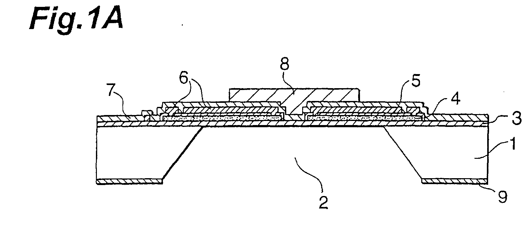
- FIG. 1A is a sectional view taken along A - A' in Fig. 1B.
- the support member of a diaphragm structure has a silicon substrate 1 having a concavity 2, and a support film 3 which supports the silicon substrate 1.
- a polysilicon film 4 in which an n- or p-type impurity is doped at 10 18 to 10 20 cm -3 and an aluminum film 6 via an SiO 2 film 5 serving as an insulating film are stacked on the support film 3.
- the polysilicon film 4 and aluminum film 6 are connected by an opening portion of the SiO 2 film 5 to form a thermocouple.
- the exposed surfaces of the support film 3 and thermocouples are coated with a passivation film 7 made of SiN.
- a infrared absorbing film 8 is formed on the passivation film 7 above the concavity 2.
- the passivation film 7 may be an insulating film such as an SiO 2 or polyimide film.
- a blackened resin is used in the infrared absorbing film 8.
- a resin epoxy, silicone, acrylic, urethane, or polyimide resin
- a black filler such as carbon filler or a black resist
- the long multi-layered structures each made of the polysilicon film 4 and aluminum film 6 range from above the silicon substrate 1 to above the concavity 2 so as to extend from four directions perpendicular to the four sides of the rectangular (square or oblong) concavity 2 toward the center of the concavity 2.
- the polysilicon film 4 and aluminum film 6 are stacked above the concavity 2.
- the width of the aluminum film 6 is smaller than that of the polysilicon film 4.
- Each polysilicon film 4 and aluminum film 6 which are stacked are connected at an opening portion of the SiO 2 film 5 in a region where the infrared absorbing film 8 is formed, thereby forming a hot junction 11.
- each polysilicon film 4 and aluminum film 6 which are adjacent to each other are connected at an opening portion of the SiO 2 film 5 above the silicon substrate 1, thereby forming a cold junction 12.
- These thermocouples are connected in series.
- An electromotive force generated by the Seebeck effect is extracted by extraction electrodes 10. In the regions where the extraction electrodes 10 are formed, the passivation film 7 is open.
- thermopile patterns, passivation film 7, and infrared absorbing film 8 are formed on a surface of the silicon substrate 1, where no concavity is formed, a mask 9 made of SiN or the like that is resistant against a silicon etchant is formed on a surface (lower surface) of a silicon substrate 1 on the opposite side to the surface with the support film 3.
- the mask 9 in a region where the concavity 2 should be formed is opened, and etching is performed while protecting the surface of the silicon substrate 1. Etching starts from the opening portion of the mask 9 on the lower surface. Etching stops at the support film 3 which is resistant against the etchant.
- the etchant for example, potassium hydroxide solution is used.
- a (100) plane is used as the silicon substrate 1, anisotropic etching can be performed.
- a diaphragm structure having the concavity 2 shown in Fig. 1(a) can be formed.
- the support film 9 may be a single SiN layer, a single SiO 2 layer, or a multi-layered film containing any one of SiN, SiO 2 , PSG, and BPSG, and its thickness is 0.5 to 5 ⁇ m.
- thermocouples can be laid out at a high density.
- thermopile pattern in which the polysilicon film 4 and aluminum film 6 are stacked via the SiO 2 film 5 has a higher mechanical support strength because of its three-layered structure. Since this structure is formed into a mesa shape ranging from above the concavity 2 to above the silicon substrate 1, the mechanical strength of the concavity 2 can be increased.
- the single lump of infrared absorbing film 8 made of a material having an adhesive force adheres the support film 3 and all the thermopile patterns above the concavity 2, the mechanical strength in a region with a small thickness at the concavity 2 can be further increased. Furthermore, since the infrared absorbing film 8 is formed to cover all the hot junctions 11 of the thermopile patterns, heat generated in the infrared absorbing film 8 due to absorption of infrared rays can be efficiently transmitted to the hot junctions 11.
- the aluminum film 6 may fail to transmit heat obtained at a hot junction to the silicon substrate 1 because of a high thermal conductivity and degrade the sensitivity of the infrared sensor.
- the thin and narrow aluminum film 6 is stacked on the polysilicon film 4 via the SiO 2 film 5 and therefore thermally insulated from the silicon substrate 1, the sensitivity of the infrared sensor does not degrade.
- the SiO 2 film 5 not only electrically insulates the polysilicon film 4 from the aluminum film 6 but also has a thermal insulating function for preventing heat transmission from the polysilicon film 4 to the aluminum film 6.
- the sensitivity of the infrared sensor may degrade. However, since the aluminum film 6 is formed narrow, reflection can be minimized. Since the reflected infrared rays are further absorbed by the infrared absorbing film 8, the sensitivity of the infrared sensor does not degrade.
- the first embodiment is not limited to this.
- the shape of the concavity 2 is not limited to a rectangular shape and may be a circular shape.
- the thermopile patterns can be formed in accordance with the shape.
- thermopile patterns of an infrared sensor according to the second embodiment are shown in Fig. 2.
- the infrared sensor of the second embodiment is obtained by widening the polysilicon film 4 of the infrared sensor of the first embodiment shown in Fig. 1B and tapering the distal end of the polysilicon film 4 above the concavity 2.
- thermoelectronic material When a semiconductor material such as polysilicon is used as a thermoelectronic material, the resistance of the thermopile increases because of the high resistivity, and accordingly, noise increases.
- the infrared sensor of the second embodiment since a polysilicon film 4 and an aluminum film 6 are stacked, the width of the polysilicon film 4 can be increased in each of thermocouples in number equal to or more than the prior art shown in Fig. 7. Hence, the resistance of the thermocouple can be reduced, and the S/N ratio can be increased by suppressing thermal noise.
- a design is also possible in which the number of thermocouples is increased (not shown) as compared to the prior art shown in Fig. 7 while keeping the resistance value of each thermocouple unchanged.
- the S/N ratio can be increased.
- the distal end of the polysilicon film 4 above a concavity 2 is tapered such that the distal end of the polysilicon film 4 can enter the center of the concavity 2, hot junctions 11 can concentrate on the center of the concavity 2. Accordingly, the degree of increase in temperature at the hot junctions becomes large, and the sensitivity increases.
- the area of the polysilicon film 4 above the concavity 2 increases, the mechanical strength in a region with a small thickness at the concavity 2 can be further increased.
- the width of the polysilicon film 4 of the infrared sensor of the first embodiment is increased, and the distal end of the polysilicon film 4 above the concavity 2 is tapered. Since the structures of the thermocouple and the like are the same as in the first embodiment, the infrared sensor can obtain the same effect as that of the first embodiment.
- the shape according to the second embodiment i.e., the tapered shape of the distal end of the polysilicon film 4 above the concavity 2 can be applied not only to this embodiment but also to other embodiments to obtain the same effect as in the second embodiment.
- thermopile patterns of an infrared sensor according to the third embodiment are shown in Figs. 3A and 3B.
- the infrared sensor of the third embodiment is obtained by changing the shape of the concavity 2 of the infrared sensor according to the first embodiment shown in Fig. 1A. More specifically, as shown in Fig. 3A that shows a section taken along B - B' in Fig. 3B, in the third embodiment, the lower side of a concavity 2 is closed by a silicon substrate 1, etching holes 13 are formed at four portions of a passivation film 7 on an upper surface, and the concavity 2 is formed under the support film 3, unlike the first embodiment in which the lower side of the concavity 2 is open.
- a method of forming the concavity 2 in the infrared sensor of the third embodiment will be described.
- a polysilicon sacrificial layer (not shown) having the same size as that of the concavity 2 is formed on the support film 3 side of a silicon substrate 1.
- thermopile patterns, and passivation film 7 are formed, the support film 3 and passivation film 7 are opened to form the etching holes 13, as shown in Fig. 3B.
- a mask 9 is formed on the lower surface of the silicon substrate 1, though the mask 9 is not opened, unlike the first embodiment.
- etching is performed by using a (100) plane as the silicon substrate 1.
- the etchant sinks from the etching holes 13 into the polysilicon sacrificial layer to entirely etch the polysilicon sacrificial layer.
- anisotropic etching of the silicon substrate 1 is started. With this process, a diaphragm structure having the concavity 2 shown in Fig. 3A can be formed. Note that etching is performed to a depth of 2 to 10 ⁇ m.
- the infrared sensor of the third embodiment only the shape of the concavity 2 is different from that of the first embodiment while the thermopile pattern is the same as in the first embodiment. Hence, the infrared sensor can obtain the same effect as that of the first embodiment.
- the infrared sensor of the third embodiment since the lower side is closed by the silicon substrate 1, die bonding to a support member such as a lead frame is easy, and the mechanical strength increases.
- the third embodiment is not limited to this.
- the shape of the concavity 2 is not limited to a rectangular shape and may be a circular shape.
- the thermopile patterns can be formed in accordance with the shape.
- the shape and positions of the etching holes 13 are not limited to those shown in Fig.
- the thickness of the polysilicon sacrificial layer is 0.3 to 1.5 ⁇ m.
- thermocouples are formed perpendicular to the four sides of the oblong concavity 2.
- thermocouples are formed to extend from two directions perpendicular to only two opposing sides of a rectangular concavity 2 toward the center of the concavity 2.
- the distance between the opposing thermopile patterns extending from the two directions to the center of the concavity 2 is 2 to 40 ⁇ m. When this distance is made as short as possible, the degree of increase in temperature at hot junctions becomes large, and the sensitivity can be increased.
- thermopile patterns of the infrared sensor are different from those of the first embodiment while the structures of the thermocouple and the like are the same as in the first embodiment.
- the infrared sensor can obtain the same effect as that of the first embodiment.
- the infrared sensors of the first to third embodiments are especially suitable for a case wherein the irradiation spot of infrared rays has a concentric circular shape
- the infrared sensor of the fourth embodiment is suitable for a case wherein the irradiation spot of infrared rays has a linear or elongated shape.
- the fourth embodiment is not limited to this.
- the shape and forming method of the concavity 2 may be the same as in the third embodiment.
- thermopile patterns of an infrared sensor according to the fifth embodiment is shown in Fig. 5.
- the infrared sensor of the fifth embodiment the infrared sensor of the third embodiment shown in Fig. 3B is used as one unit 20, and the units 20 are arranged in a one-dimensional array on a single silicon substrate 1.
- one of extraction electrodes 10 shown in Fig. 3B is connected as a common electrode of the units, and a common extraction electrode 15 is arranged.
- the difference in infrared irradiation intensity between positions can be measured.
- the infrared sensor of one unit has the same structure as in the third embodiment, the same effect as that of the third embodiment can be obtained.
- the fifth embodiment is not limited to this.
- one unit is arranged in a one-dimensional array.
- the units may be arranged in a two-dimensional array. With this arrangement, the difference in infrared irradiation intensity between two-dimensional positions can be measured.
- thermopile patterns of an infrared sensor according to the sixth embodiment are shown in Fig. 6.
- the infrared sensor of the fourth embodiment shown in Fig. 4B is used as one unit 30, and the units 30 are arranged in a one-dimensional array on a single silicon substrate 1.
- one of extraction electrodes 10 shown in Fig. 4B is connected as a common electrode of the units, and a common extraction electrode 15 is arranged.
- the difference in infrared irradiation intensity between positions can be measured.
- the infrared sensor of one unit has the same structure as in the fourth embodiment, the same effect as that of the fourth embodiment can be obtained.
- the sixth embodiment is not limited to this.
- one unit is arranged in a one-dimensional array.
- the units may be arranged in a two-dimensional array. With this arrangement, the difference in infrared irradiation intensity between two-dimensional positions can be measured.
- thermocouple is formed by stacking a polysilicon interconnection layer and an aluminum interconnection layer, the layout region of the thermocouple is small, and the layout density can be increased. Since the multilayered structure of the polysilicon interconnection layer and aluminum interconnection layer ranges from above a concavity to above a substrate, the mechanical strength of the thin concavity can be increased. Since a plurality of multilayered structures each including a polysilicon interconnection layer and an aluminum interconnection layer via an insulating film are formed, and the plurality of multilayered structures function as a support structure integral with an infrared absorption layer, the mechanical strength of the thin concavity can be further increased. Since the infrared absorption layer is formed to cover first junction hole formed in the thermocouples, heat generated in the infrared absorption layer can be efficiently transmitted to the thermocouples.
Landscapes
- Physics & Mathematics (AREA)
- General Physics & Mathematics (AREA)
- Spectroscopy & Molecular Physics (AREA)
- Photometry And Measurement Of Optical Pulse Characteristics (AREA)
- Radiation Pyrometers (AREA)
Abstract
Description
Claims (4)
- An infrared sensor characterized by comprising:wherein said aluminum interconnection layer connected to said corresponding polysilicon interconnection layer through the first junction hole is stacked via said insulating film as an overlying layer of said corresponding polysilicon interconnection layer above the concavity.a support member including a support film made of an insulating material and a substrate that has a concavity and supports the support film;a polysilicon interconnection layer which has a predetermined conductivity type and ranges from above the concavity to above the substrate;an insulating film which is formed on said polysilicon interconnection layer and has a first junction hole formed above the concavity and a second junction hole formed above the substrate;an aluminum interconnection layer which is connected to said polysilicon interconnection layer through the first junction hole and connected to an adjacent polysilicon interconnection layer through the second junction hole; andan infrared absorption layer formed above the concavity to cover a portion above the first junction hole,
- An infrared sensor according to claim 1, characterized in that the substrate is made of silicon, and the concavity is formed by etching.
- An infrared sensor according to claim 1 or 2, characterized in that said aluminum interconnection layer is formed to be narrower than said polysilicon interconnection layer at least above the concavity.
- An infrared sensor according to any one of claims 1 to 3, characterized in that a plurality of multilayered structures each of which has said aluminum interconnection layer stacked on said polysilicon interconnection layer via said insulating film are formed, and the plurality of first junction holes are covered with said infrared absorption layer integrally formed.
Applications Claiming Priority (1)
| Application Number | Priority Date | Filing Date | Title |
|---|---|---|---|
| PCT/JP2001/003077 WO2002084235A1 (en) | 2001-04-10 | 2001-04-10 | Infrared sensor |
Publications (3)
| Publication Number | Publication Date |
|---|---|
| EP1378733A1 true EP1378733A1 (en) | 2004-01-07 |
| EP1378733A4 EP1378733A4 (en) | 2007-03-21 |
| EP1378733B1 EP1378733B1 (en) | 2009-09-16 |
Family
ID=29727309
Family Applications (1)
| Application Number | Title | Priority Date | Filing Date |
|---|---|---|---|
| EP01919861A Expired - Lifetime EP1378733B1 (en) | 2001-04-10 | 2001-04-10 | Infrared sensor |
Country Status (8)
| Country | Link |
|---|---|
| US (1) | US7282712B2 (en) |
| EP (1) | EP1378733B1 (en) |
| JP (1) | JP4009046B2 (en) |
| KR (1) | KR100794067B1 (en) |
| CN (2) | CN100462697C (en) |
| DE (1) | DE60139958D1 (en) |
| TW (1) | TWI248513B (en) |
| WO (1) | WO2002084235A1 (en) |
Families Citing this family (57)
| Publication number | Priority date | Publication date | Assignee | Title |
|---|---|---|---|---|
| JP4009046B2 (en) * | 2001-04-10 | 2007-11-14 | 浜松ホトニクス株式会社 | Infrared sensor |
| DE10144343A1 (en) * | 2001-09-10 | 2003-03-27 | Perkinelmer Optoelectronics | Sensor for contactless measurement of a temperature |
| DE10144873A1 (en) * | 2001-09-12 | 2003-03-27 | Bosch Gmbh Robert | Micromechanical heat conductivity sensor used for analyzing gas mixtures containing hydrogen and/or helium has a thermally insulating membrane covered on one or both of its sides by a porous covering plate which permits gas diffusion |
| JP4496751B2 (en) * | 2003-10-09 | 2010-07-07 | 日本電気株式会社 | Thermal infrared solid-state imaging device and manufacturing method thereof |
| JP2005241457A (en) * | 2004-02-26 | 2005-09-08 | Hamamatsu Photonics Kk | Infrared sensor and manufacturing method thereof |
| JP2005283435A (en) * | 2004-03-30 | 2005-10-13 | Japan Aviation Electronics Industry Ltd | Infrared sensor |
| DE102004028032B4 (en) * | 2004-06-09 | 2008-04-17 | Perkinelmer Optoelectronics Gmbh & Co.Kg | sensor element |
| DE102004030418A1 (en) * | 2004-06-24 | 2006-01-19 | Robert Bosch Gmbh | Microstructured infrared sensor and a method for its production |
| JP2006071601A (en) * | 2004-09-06 | 2006-03-16 | Denso Corp | Infrared sensor, infrared gas detector, and infrared light source |
| JP5102436B2 (en) * | 2005-01-21 | 2012-12-19 | 日本セラミック株式会社 | Thermopile array manufacturing method |
| US7785002B2 (en) * | 2006-12-05 | 2010-08-31 | Delphi Technologies, Inc. | P-N junction based thermal detector |
| DE102007038726B4 (en) * | 2007-08-16 | 2009-07-09 | Universität Bremen | Thin-film thermocouple assembly, thermoelectric sensor, thermal generator, and method of making the thin-film thermocouple assembly |
| JP2009174917A (en) * | 2008-01-22 | 2009-08-06 | Oki Semiconductor Co Ltd | Infrared detecting element and method for manufacturing infrared detecting element |
| DE102008006245A1 (en) * | 2008-01-25 | 2009-07-30 | Nirlus Engineering Ag | Method for the noninvasive, optical determination of the temperature of a medium |
| US8262236B2 (en) | 2008-06-17 | 2012-09-11 | The Invention Science Fund I, Llc | Systems and methods for transmitting information associated with change of a projection surface |
| US8641203B2 (en) | 2008-06-17 | 2014-02-04 | The Invention Science Fund I, Llc | Methods and systems for receiving and transmitting signals between server and projector apparatuses |
| US8384005B2 (en) | 2008-06-17 | 2013-02-26 | The Invention Science Fund I, Llc | Systems and methods for selectively projecting information in response to at least one specified motion associated with pressure applied to at least one projection surface |
| US8820939B2 (en) | 2008-06-17 | 2014-09-02 | The Invention Science Fund I, Llc | Projection associated methods and systems |
| US20090309826A1 (en) | 2008-06-17 | 2009-12-17 | Searete Llc, A Limited Liability Corporation Of The State Of Delaware | Systems and devices |
| US8944608B2 (en) | 2008-06-17 | 2015-02-03 | The Invention Science Fund I, Llc | Systems and methods associated with projecting in response to conformation |
| US8608321B2 (en) | 2008-06-17 | 2013-12-17 | The Invention Science Fund I, Llc | Systems and methods for projecting in response to conformation |
| US8267526B2 (en) | 2008-06-17 | 2012-09-18 | The Invention Science Fund I, Llc | Methods associated with receiving and transmitting information related to projection |
| US8602564B2 (en) | 2008-06-17 | 2013-12-10 | The Invention Science Fund I, Llc | Methods and systems for projecting in response to position |
| US8308304B2 (en) | 2008-06-17 | 2012-11-13 | The Invention Science Fund I, Llc | Systems associated with receiving and transmitting information related to projection |
| US8723787B2 (en) | 2008-06-17 | 2014-05-13 | The Invention Science Fund I, Llc | Methods and systems related to an image capture projection surface |
| US8733952B2 (en) | 2008-06-17 | 2014-05-27 | The Invention Science Fund I, Llc | Methods and systems for coordinated use of two or more user responsive projectors |
| US8936367B2 (en) | 2008-06-17 | 2015-01-20 | The Invention Science Fund I, Llc | Systems and methods associated with projecting in response to conformation |
| US8430515B2 (en) | 2008-06-17 | 2013-04-30 | The Invention Science Fund I, Llc | Systems and methods for projecting |
| KR101008260B1 (en) * | 2008-06-27 | 2011-01-13 | (주)엔아이디에스 | Infrared sensor and its manufacturing method |
| DE102008041131B4 (en) * | 2008-08-08 | 2020-07-30 | Robert Bosch Gmbh | Thermopile sensor for the detection of infrared radiation |
| CN102197291A (en) * | 2008-09-25 | 2011-09-21 | 松下电工株式会社 | Infrared sensor |
| US8304851B2 (en) | 2010-03-30 | 2012-11-06 | Texas Instruments Incorporated | Semiconductor thermocouple and sensor |
| JP2013524541A (en) * | 2010-04-14 | 2013-06-17 | エクセリタス カナダ,インコーポレイテッド | Laminated thermopile |
| WO2011136203A1 (en) | 2010-04-26 | 2011-11-03 | 株式会社エッチ.エム.イー. | Temperature sensor device and radiation thermometer using same, method for producing temperature sensor device, multilayered thin film thermopile using photoresist film and radiation thermometer using same, and method for producing multilayered thin film thermopile |
| JP5558189B2 (en) * | 2010-04-26 | 2014-07-23 | 浜松ホトニクス株式会社 | Infrared sensor and manufacturing method thereof |
| US8441093B2 (en) * | 2011-04-15 | 2013-05-14 | Excelitas Technologies Singapore Pte. Ltd. | Shared membrane thermopile sensor array |
| TWI452272B (en) * | 2011-05-24 | 2014-09-11 | Univ Nat Kaohsiung Applied Sci | Thermopile sensing element |
| GB201112430D0 (en) * | 2011-07-20 | 2011-08-31 | Melexis Tessenderlo Nv | IR sensor design |
| CN102322961B (en) * | 2011-07-27 | 2017-02-22 | 中国科学院上海微系统与信息技术研究所 | Micromachine thermopile infrared sensor with high duty cycle and manufacture method thereof |
| US9784577B2 (en) * | 2012-03-16 | 2017-10-10 | Lg Innotek Co., Ltd. | Measuring distance from object by using size of pattern projected onto object |
| US9219185B2 (en) | 2013-12-19 | 2015-12-22 | Excelitas Technologies Singapore Pte. Ltd | CMOS integrated method for the fabrication of thermopile pixel with umbrella absorber on semiconductor substrate |
| US9373772B2 (en) | 2014-01-15 | 2016-06-21 | Excelitas Technologies Singapore Pte. Ltd. | CMOS integrated method for the release of thermopile pixel on a substrate by using anisotropic and isotropic etching |
| US9324760B2 (en) * | 2014-01-21 | 2016-04-26 | Excelitas Technologies Singapore Pte. Ltd | CMOS integrated method for fabrication of thermopile pixel on semiconductor substrate with buried insulation regions |
| JP6467172B2 (en) * | 2014-09-16 | 2019-02-06 | ヤマハファインテック株式会社 | Contact combustion type gas sensor |
| TWI569427B (en) * | 2014-10-22 | 2017-02-01 | 精材科技股份有限公司 | Semiconductor package and its manufacturing method |
| CN104501983B (en) * | 2015-01-08 | 2017-03-22 | 上海新微技术研发中心有限公司 | A pleated film temperature sensor and its manufacturing method |
| JP6467254B2 (en) * | 2015-03-16 | 2019-02-06 | ヤマハファインテック株式会社 | Infrared sensor |
| US10203252B2 (en) | 2016-12-29 | 2019-02-12 | Industrial Technology Research Institute | Microelectromechanical apparatus having a measuring range selector |
| CA3213747A1 (en) | 2018-10-12 | 2020-04-16 | Amphenol Thermometrics, Inc. | Ndir sensor, sampling method and system for breath analysis |
| US11480479B2 (en) * | 2019-02-04 | 2022-10-25 | The Board Of Trustees Of The University Of Illinois | Microscale thermocouple probe for intracellular temperature measurements |
| WO2020195466A1 (en) * | 2019-03-27 | 2020-10-01 | パナソニックIpマネジメント株式会社 | Infrared sensor and infrared sensor device equipped with same |
| JP7428186B2 (en) * | 2019-07-05 | 2024-02-06 | 住友電気工業株式会社 | light sensor |
| JP7258800B2 (en) * | 2020-03-02 | 2023-04-17 | Mmiセミコンダクター株式会社 | Thermopile type sensor |
| RU2752728C1 (en) * | 2021-01-18 | 2021-07-30 | Федеральное государственное казенное учреждение "12 Центральный научно-исследовательский институт" Министерства обороны Российской Федерации | Device for measuring energy parameters of light radiation |
| EP4339568A4 (en) * | 2021-05-11 | 2024-10-09 | Panasonic Intellectual Property Management Co., Ltd. | INFRARED SENSOR AND METHOD FOR MANUFACTURING THE INFRARED SENSOR |
| JP7818270B2 (en) * | 2022-03-24 | 2026-02-20 | 国立研究開発法人産業技術総合研究所 | Heat flow sensor utilizing the anomalous Nernst effect and its manufacturing method |
| JP2024056365A (en) * | 2022-10-11 | 2024-04-23 | 住友電気工業株式会社 | Optical Sensor |
Family Cites Families (16)
| Publication number | Priority date | Publication date | Assignee | Title |
|---|---|---|---|---|
| JP2663612B2 (en) | 1989-02-09 | 1997-10-15 | 日産自動車株式会社 | Infrared sensor |
| JPH0377031A (en) * | 1989-08-18 | 1991-04-02 | Anritsu Corp | Radiation wave detecting element |
| JPH0760120B2 (en) | 1989-09-30 | 1995-06-28 | アンリツ株式会社 | Optical power sensor |
| US5059543A (en) * | 1990-09-21 | 1991-10-22 | The Board Of Regents Acting For And On Behalf Of The University Of Michigan | Method of manufacturing thermopile infrared detector |
| US5100479A (en) * | 1990-09-21 | 1992-03-31 | The Board Of Regents Acting For And On Behalf Of The University Of Michigan | Thermopile infrared detector with semiconductor supporting rim |
| KR100205384B1 (en) | 1997-03-14 | 1999-07-01 | 구자홍 | Infrared sensor and method of temperature compensation |
| DE19710946A1 (en) * | 1997-03-15 | 1998-09-24 | Braun Ag | Thermopile sensor and radiation thermometer with a thermopile sensor |
| KR100239494B1 (en) * | 1998-02-28 | 2000-01-15 | 구자홍 | Thermopile sensor and method for fabricating the same |
| JPH11258055A (en) | 1998-03-12 | 1999-09-24 | Omron Corp | Thermopile type temperature sensor |
| US6348650B1 (en) * | 1999-03-24 | 2002-02-19 | Ishizuka Electronics Corporation | Thermopile infrared sensor and process for producing the same |
| JP3399399B2 (en) * | 1999-04-14 | 2003-04-21 | 株式会社村田製作所 | Infrared sensor and method of manufacturing the same |
| DE19932308C2 (en) * | 1999-07-10 | 2001-10-25 | Bosch Gmbh Robert | Sensor, especially thermal sensor |
| US6300554B1 (en) * | 1999-09-09 | 2001-10-09 | Metrodyne Microsystem Corp. | Method of fabricating thermoelectric sensor and thermoelectric sensor device |
| JP3388207B2 (en) * | 1999-09-10 | 2003-03-17 | 全磊微機電股▲ふん▼有限公司 | Thermoelectric sensor device and method of manufacturing the same |
| DE10033589A1 (en) * | 2000-07-11 | 2002-01-31 | Bosch Gmbh Robert | Microstructured thermal sensor |
| JP4009046B2 (en) * | 2001-04-10 | 2007-11-14 | 浜松ホトニクス株式会社 | Infrared sensor |
-
2000
- 2000-01-18 JP JP2000009420A patent/JP4009046B2/en not_active Expired - Fee Related
-
2001
- 2001-04-09 TW TW090108589A patent/TWI248513B/en not_active IP Right Cessation
- 2001-04-10 CN CNB200510117316XA patent/CN100462697C/en not_active Expired - Fee Related
- 2001-04-10 EP EP01919861A patent/EP1378733B1/en not_active Expired - Lifetime
- 2001-04-10 CN CNB018221939A patent/CN1236292C/en not_active Expired - Lifetime
- 2001-04-10 WO PCT/JP2001/003077 patent/WO2002084235A1/en not_active Ceased
- 2001-04-10 DE DE60139958T patent/DE60139958D1/en not_active Expired - Lifetime
- 2001-04-10 KR KR1020037010054A patent/KR100794067B1/en not_active Expired - Fee Related
-
2003
- 2003-05-21 US US10/442,109 patent/US7282712B2/en not_active Expired - Fee Related
Also Published As
| Publication number | Publication date |
|---|---|
| KR20030091979A (en) | 2003-12-03 |
| CN1488070A (en) | 2004-04-07 |
| WO2002084235A1 (en) | 2002-10-24 |
| JP2001201397A (en) | 2001-07-27 |
| CN1758035A (en) | 2006-04-12 |
| CN1236292C (en) | 2006-01-11 |
| KR100794067B1 (en) | 2008-01-10 |
| US20030205670A1 (en) | 2003-11-06 |
| EP1378733A4 (en) | 2007-03-21 |
| EP1378733B1 (en) | 2009-09-16 |
| US7282712B2 (en) | 2007-10-16 |
| TWI248513B (en) | 2006-02-01 |
| DE60139958D1 (en) | 2009-10-29 |
| CN100462697C (en) | 2009-02-18 |
| JP4009046B2 (en) | 2007-11-14 |
Similar Documents
| Publication | Publication Date | Title |
|---|---|---|
| EP1378733B1 (en) | Infrared sensor | |
| CN100473962C (en) | Infrared array detection device | |
| US7638769B2 (en) | Solid-state image sensing device, method for manufacturing the same, and imaging system | |
| KR101624762B1 (en) | Optical sensor | |
| JPH02205729A (en) | Infrared-ray sensor | |
| JP2003166876A (en) | Thermal infrared detecting element, method of manufacturing the same, and thermal infrared detecting element array | |
| JP3186415B2 (en) | Manufacturing method of infrared detecting element | |
| JP5079211B2 (en) | Infrared detector and manufacturing method thereof | |
| JP3132197B2 (en) | Thermal infrared sensor | |
| JPH11211558A (en) | Sensors and sensor arrays | |
| JP2811709B2 (en) | Infrared sensor | |
| CN113428833A (en) | MEMS thermopile infrared sensor and preparation method thereof | |
| JP2884679B2 (en) | Thermopile type infrared sensor | |
| JP2000111396A (en) | Infrared detecting element and method of manufacturing the same | |
| JPH11191644A (en) | Infrared detector | |
| JPH046424A (en) | Infrared sensor | |
| JP3435997B2 (en) | Infrared detector | |
| JP3275593B2 (en) | Infrared detecting element and method of manufacturing the same | |
| JPH04132271A (en) | Infrared sensor | |
| JPH03276773A (en) | infrared sensor | |
| JPH0982680A (en) | Method for manufacturing semiconductor device |
Legal Events
| Date | Code | Title | Description |
|---|---|---|---|
| PUAI | Public reference made under article 153(3) epc to a published international application that has entered the european phase |
Free format text: ORIGINAL CODE: 0009012 |
|
| 17P | Request for examination filed |
Effective date: 20030625 |
|
| AK | Designated contracting states |
Kind code of ref document: A1 Designated state(s): AT BE CH CY DE DK ES FI FR GB GR IE IT LI LU MC NL PT SE TR |
|
| AX | Request for extension of the european patent |
Extension state: AL LT LV MK RO SI |
|
| A4 | Supplementary search report drawn up and despatched |
Effective date: 20070215 |
|
| 17Q | First examination report despatched |
Effective date: 20070222 |
|
| GRAP | Despatch of communication of intention to grant a patent |
Free format text: ORIGINAL CODE: EPIDOSNIGR1 |
|
| GRAS | Grant fee paid |
Free format text: ORIGINAL CODE: EPIDOSNIGR3 |
|
| GRAA | (expected) grant |
Free format text: ORIGINAL CODE: 0009210 |
|
| AK | Designated contracting states |
Kind code of ref document: B1 Designated state(s): DE FR GB |
|
| REG | Reference to a national code |
Ref country code: GB Ref legal event code: FG4D |
|
| REF | Corresponds to: |
Ref document number: 60139958 Country of ref document: DE Date of ref document: 20091029 Kind code of ref document: P |
|
| PLBE | No opposition filed within time limit |
Free format text: ORIGINAL CODE: 0009261 |
|
| STAA | Information on the status of an ep patent application or granted ep patent |
Free format text: STATUS: NO OPPOSITION FILED WITHIN TIME LIMIT |
|
| 26N | No opposition filed |
Effective date: 20100617 |
|
| PGFP | Annual fee paid to national office [announced via postgrant information from national office to epo] |
Ref country code: GB Payment date: 20140409 Year of fee payment: 14 |
|
| PGFP | Annual fee paid to national office [announced via postgrant information from national office to epo] |
Ref country code: FR Payment date: 20140409 Year of fee payment: 14 Ref country code: DE Payment date: 20140430 Year of fee payment: 14 |
|
| REG | Reference to a national code |
Ref country code: DE Ref legal event code: R119 Ref document number: 60139958 Country of ref document: DE |
|
| GBPC | Gb: european patent ceased through non-payment of renewal fee |
Effective date: 20150410 |
|
| PG25 | Lapsed in a contracting state [announced via postgrant information from national office to epo] |
Ref country code: GB Free format text: LAPSE BECAUSE OF NON-PAYMENT OF DUE FEES Effective date: 20150410 Ref country code: DE Free format text: LAPSE BECAUSE OF NON-PAYMENT OF DUE FEES Effective date: 20151103 |
|
| REG | Reference to a national code |
Ref country code: FR Ref legal event code: ST Effective date: 20151231 |
|
| PG25 | Lapsed in a contracting state [announced via postgrant information from national office to epo] |
Ref country code: FR Free format text: LAPSE BECAUSE OF NON-PAYMENT OF DUE FEES Effective date: 20150430 |