EP1376699A1 - Production method for simox substrate and simox substrate - Google Patents
Production method for simox substrate and simox substrate Download PDFInfo
- Publication number
- EP1376699A1 EP1376699A1 EP02707233A EP02707233A EP1376699A1 EP 1376699 A1 EP1376699 A1 EP 1376699A1 EP 02707233 A EP02707233 A EP 02707233A EP 02707233 A EP02707233 A EP 02707233A EP 1376699 A1 EP1376699 A1 EP 1376699A1
- Authority
- EP
- European Patent Office
- Prior art keywords
- ion implantation
- substrate
- applying
- heat treatment
- oxide layer
- Prior art date
- Legal status (The legal status is an assumption and is not a legal conclusion. Google has not performed a legal analysis and makes no representation as to the accuracy of the status listed.)
- Granted
Links
Images




Classifications
-
- H—ELECTRICITY
- H10—SEMICONDUCTOR DEVICES; ELECTRIC SOLID-STATE DEVICES NOT OTHERWISE PROVIDED FOR
- H10D—INORGANIC ELECTRIC SEMICONDUCTOR DEVICES
- H10D86/00—Integrated devices formed in or on insulating or conducting substrates, e.g. formed in silicon-on-insulator [SOI] substrates or on stainless steel or glass substrates
-
- H—ELECTRICITY
- H10—SEMICONDUCTOR DEVICES; ELECTRIC SOLID-STATE DEVICES NOT OTHERWISE PROVIDED FOR
- H10P—GENERIC PROCESSES OR APPARATUS FOR THE MANUFACTURE OR TREATMENT OF DEVICES COVERED BY CLASS H10
- H10P90/00—Preparation of wafers not covered by a single main group of this subclass, e.g. wafer reinforcement
- H10P90/19—Preparing inhomogeneous wafers
- H10P90/1904—Preparing vertically inhomogeneous wafers
- H10P90/1906—Preparing SOI wafers
- H10P90/1908—Preparing SOI wafers using silicon implanted buried insulating layers, e.g. oxide layers [SIMOX]
-
- H—ELECTRICITY
- H10—SEMICONDUCTOR DEVICES; ELECTRIC SOLID-STATE DEVICES NOT OTHERWISE PROVIDED FOR
- H10W—GENERIC PACKAGES, INTERCONNECTIONS, CONNECTORS OR OTHER CONSTRUCTIONAL DETAILS OF DEVICES COVERED BY CLASS H10
- H10W10/00—Isolation regions in semiconductor bodies between components of integrated devices
- H10W10/10—Isolation regions comprising dielectric materials
- H10W10/181—Semiconductor-on-insulator [SOI] isolation regions, e.g. buried oxide regions of SOI wafers
Definitions
- the present invention relates to an SOI substrate having a buried oxide layer near a surface of a silicon substrate and a single crystal silicon surface layer (hereinafter called an SOI layer, meaning a silicon-on-insulator layer) formed thereon.
- an SOI layer meaning a silicon-on-insulator layer
- a Separation by Implanted OXygen (SIMOX) wafer and a bonded wafer are known as typical examples of an SOI substrate which has a single crystal silicon layer formed on an insulating material such as silicon dioxide.
- the SIMOX wafer is an SOI substrate obtained by: introducing oxygen ions inside a single crystal silicon substrate through the ion implantation of oxygen ions; having the oxygen ions react with silicon atoms through a subsequent annealing process; and thus forming a Buried OXide layer (hereinafter called a BOX layer).
- the bonded wafer is an SOI substrate obtained by: bonding two single crystal silicon wafers, with an oxide layer in between; and then turning one of the two wafers into a thin film.
- a Metal-Oxide-Semiconductor Field Effect Transistor (MOSFET) formed in the SOI layer of such an SOI substrate has high radiation resistance and high latch-up resistance, shows high reliability, suppresses a short channel effect which tends to occur as a device size becomes smaller, and enables an operation with low power consumption, as well. Besides, because the operating region of a device is isolated from the substrate itself in terms of dielectric capacitance, signal transmission speed is enhanced, and thus high-speed operation of the device is realized. For those reasons, the SOI substrate has been the most promising canditate of a high performance semiconductor substrate for MOS-LSIs of the next generation.
- the SIMOX wafer has an advantage in its excellent uniformity of the thickness of the SOI layer.
- An SOI layer 0.1 ⁇ m or less in thickness, in particular, is often used for forming a MOS-LSI for fully depletion type operation.
- the uniformity of the thickness of the SOI layer constitutes an important quality aspect for producing devices of uniform performance at a high yield.
- the SIMOX wafer having an SOI layer excellent in uniformity of the thickness has been the most promising canditate of the substrates for MOSFETs of the next generation.
- a MOS-LSI formed on an SOI substrate is capable of realizing the excellent properties described above, such as the enhanced radiation resistance and latch-up resistance, the operation with low power consumption, the ultra-high-speed operation, etc., thanks to the fact that the device active area is dielectrically isolated from the substrate itself by laying the BOX layer which is an insulator between them.
- the BOX layer is required to have as perfect an insulating property as possible. More concretely, it is required that the leak defects in the BOX layer (hereinafter called pinhole defects) are as small as possible and the dielectric breakdown property is as close to that of a thermally-grown oxide layer as possible.
- oxygen ions are implanted by applying, usually, a fixed amount of accelerating energy, typically, an accelerating voltage of 200 kV or so. It is widely known that, in the SIMOX structure formed after a high temperature heat treatment, a continuous, uniform and high quality BOX layer can be obtained only when the implantation dosing amount of the oxygen ions is 1.5 x 10 18 cm -2 or more, or within a limited range from 2.5 to 4.5 x 10 17 cm -2 (refer to S. Nakashima and K. Izumi, the Journal of Materials Research, Vol. 8, p.523 (1993), for example).
- the SIMOX wafer produced by implanting the oxygen ion amount specified above is conventionally called: a high dose SIMOX substrate when produced by implanting the oxygen ion amount in the former range; or a low dose SIMOX substrate when produced by implanting the oxygen ion amount in the latter range.
- the high dose SIMOX substrate and the low dose SIMOX substrate have respective characteristics, and they are used for different applications according to the characteristics.
- the dosing amount of oxygen ion implantation is comparatively small, therefore the threading dislocation density of the SOI layer is decreased, and the low dose SIMOX substrate is expected to be a technology capable of realizing low-cost production.
- the low dose SIMOX substrate however, has problems such as the relatively large density of pinhole defects in the BOX layer, the high probability of dielectric breakdown property of the BOX layer becoming insufficient and so forth, because the BOX layer is thin.
- the BOX quality of the low dose SIMOX substrate when it is attempted to increase the thickness of the BOX layer by simply increasing the oxygen ion implantation amount, although the pinhole defects decrease, granular substances consisted of silicon (hereinafter called silicon islands) are generated in quantities inside the BOX layer and, as a result, the breakdown electric field of the BOX layer is lowered.
- silicon islands granular substances consisted of silicon (hereinafter called silicon islands) are generated in quantities inside the BOX layer and, as a result, the breakdown electric field of the BOX layer is lowered.
- the oxygen ion implantation dosing amount is decreased, in contrast, though the silicon islands decrease and the breakdown electric field of the BOX layer is improved, the density of the pinhole defects increases as the oxygen ion implantation dosing amount decreases. It has therefore been very difficult to simultaneously improve the whole quality of the BOX layer in the low dose SIMOX substrate produced according to a conventional technology.
- ITOX technology internal thermal oxidation process
- a thermally-grown oxide layer grows on the substrate surface through an oxidation treatment at a high temperature, and, at the same time, some amount of thermally-grown oxide layer at the upper interface of the BOX layer, and thus it becomes possible to make the BOX layer thicker. Further, it has been reported that the pinhole defects are decreased as a result, and the breakdown electric field is improved at the same time.
- the surface oxide layer it is necessary for the surface oxide layer to grow by not less than 10 times the increase in the thickness of the BOX layer. For this reason, to secure a prescribed thickness of the SOI layer in the SIMOX structure finally obtained, it is necessary to restrict the amount of oxidation of the substrate surface. As a consequence, there has been a natural limit in the increment of the BOX layer thickness.
- the SOI layer finally obtained tends to be thin.
- the proposed technology is, therefore, not suitable for increasing the thickness of the BOX layer while maintaining the thickness of the SOI layer.
- the object of the present invention is to provide a technology capable of increasing the thickness of the buried oxide layer of the SIMOX substrate without the above difficulties.
- the object of the present invention is to provide a high quality SOI substrate for a high performance LSI by making it possible to increase the thickness of the BOX layer of a SIMOX substrate produced by employing the oxygen ion implantation amount in the low dose range, keeping good quality of the BOX layer, and a method of producing the SOI substrate.
- the present inventors newly discovered that it is possible to increase the thickness of the BOX layer, while maintaining the thickness and crystallinity of the SOI layer and suppressing the formation of the silicon islands in the BOX layer, if, after a BOX layer is once formed through a high temperature heat treatment, oxygen ions are implanted again in a position deeper than the BOX layer thus formed and then a heat treatment at a high temperature is applied once again.
- the present invention therefore, relates to a method of producing an SOI substrate which solves the above problems and, further, to the SOI substrate produced by applying the technologies of the method, and it is realized by the following means.
- a method of producing a SIMOX substrate wherein a BOX layer and an SOI layer are formed by applying the implantation of oxygen ions into a silicon substrate and a heat treatment at a high temperature thereafter characterized by: forming a BOX layer through applying a high temperature heat treatment after an oxygen ion implantation; and then, repeatedly, applying oxygen ion implantation so that the peak position of the distribution of implanted oxygen is located at a portion lower than the interface between the BOX layer, already formed, and the substrate thereunder, and a heat treatment at a high temperature thereafter.
- a method of producing a SIMOX substrate according to the above characterized in that the dosing amount of an additional oxygen ion implantation does not exceed the total dosing amount of the oxygen ions implanted earlier.
- a method of producing a SIMOX substrate according to the above characterized in that the accelerating energy applied to the oxygen ion implantation is different from that applied to an additional oxygen ion implantation.
- a method of producing a SIMOX substrate according to the above characterized by partially removing the surface of the SOI layer already formed before the additional oxygen ion implantation.
- a method of producing a SIMOX substrate according to the above characterized in that the method of removing the surface of the SOI layer is etching using a reactive substance.
- a method of producing a SIMOX substrate according to the above characterized in that the method of removing the surface of the SOI layer is the removal of an oxide layer after forming it by oxidizing the surface of the substrate.
- the number of repetitions of the oxygen ion implantation and the high temperature heat treatment is two.
- any of the methods of producing a SIMOX substrate according to the above it is desirable to form an oxide layer on the surface of the silicon substrate prior to the oxygen ion implantation and to remove the oxide layer after the oxygen ion implantation or the high temperature heat treatment.
- the oxygen ion implantation is conducted under a condition of an accelerating energy of 150 to 250 keV and a dosing amount of 2 to 6 x 10 17 cm -2 , that an additional oxygen ion implantation is conducted under a condition of an accelerating energy of 150 to 250 keV and a dosing amount of 0.1 to 6 x 10 17 cm- 2 , and that the total depth of the removal of the silicon surface is 20 to 300 nm.
- the present invention is, further, a SIMOX substrate produced by applying any of the methods according to the above, characterized in that the thickness of the SOI layer of the SIMOX substrate is 10 to 400 nm and the thickness of the BOX layer thereof is 60 to 250 nm.
- a BOX layer similar to that of a conventional low dose SIMOX substrate is once formed through an oxygen ion implantation and a high temperature heat treatment. For this reason, when the oxygen implanted at an additional oxygen ion implantation precipitates during the subsequent high temperature heat treatment, the precipitation takes place stably, because the BOX layer already formed exists and the precipitating oxygen is absorbed in the BOX layer. As a result, it is possible to obtain a single BOX layer stably.
- the first half of the processes to produce a SIMOX substrate according to an embodiment of the present invention employs the production processes of the SIMOX substrate according to a conventional technology shown in Fig. 1.
- an oxygen implanted zone 2' is formed by charging a single crystal silicon substrate 1 into an ion implantation apparatus and implanting oxygen ions up to a prescribed dosing amount in the surface of the substrate, while heating the substrate so as to maintain its crystallinity. Then, the substrate is discharged from the ion implantation apparatus and, 2) a SIMOX structure having an SOI layer 3' and a BOX layer 4' is formed by applying a high temperature heat treatment in a heat treatment furnace.
- an oxygen ion implanted zone 2 is formed by applying oxygen ion implantation under such an accelerating voltage that the peak of the distribution of the implanted oxygen ions is located at the lower portion of the already formed BOX layer 4'.
- the substrate is discharged from the ion implantation apparatus and, then, 4) a SIMOX structure having an SOI layer 3 and a BOX layer 4 is formed by applying a high temperature heat treatment in a heat treatment furnace.
- the oxygen ion implantation and the high temperature heat treatment described above are called the second oxygen ion implantation and the second high temperature heat treatment, respectively, in the explanations of this description.
- the oxygen ions implanted at the second oxygen ion implantation aggregate onto the already formed BOX layer 4' from the lower side during the subsequent second high temperature heat treatment.
- the precipitation of the oxygen ions proceeds during the second high temperature heat treatment so that the oxygen ions implanted at the second oxygen ion implantation aggregate in priority to the BOX layer 4' already formed, without precipitating them independently.
- the BOX layer 4 is made thicker, maintaining good uniformity of the thickness of the SOI layer.
- the damage inflicted on the material wherein ions are implanted by the implanted ions becomes larger as the ions lose their energy and decelerate in the material wherein ions are implanted.
- the degree of the damage inflicted on the material wherein ions are implanted by the implanted ions therefore, becomes large at the vicinity immediately above the position where the ions halt.
- the SOI layer 3' is made thinner by removing a part of its surface.
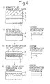
- the substrate is charged into the ion implantation apparatus again and 4) oxygen ion implantation is carried out by applying such an accelerating voltage that the peak of the distribution of implanted oxygen ions is located at the lower portion of the already formed BOX layer 4' as shown in Fig. 2.
- the substrate is discharged from the ion implantation apparatus and, then, a SIMOX structure having an SOI layer 3 and a BOX layer 4 is formed by applying a high temperature heat treatment in a heat treatment furnace.
- a thermally-grown oxide layer 5 is formed on the surface of the SOI layer 3', and then 4) the oxide layer is removed.
- a solvent to selectively dissolve the oxide layer or the like may be used for the removal.
- a SIMOX structure having an SOI layer 3 and a BOX layer 4 is formed by applying 5) an ion implantation in the same manner as in Fig. 2 and 6) a heat treatment.
- the first to third embodiments of the present invention shown in Figs. 2 to 4, respectively, are examples wherein the oxygen ion implantation is repeated twice in total, but the partial removal of the SOI layer and the subsequent oxygen ion implantation and high temperature heat treatment may be repeated as long as the SOI layer does not disappear.
- an accelerating voltage of 150 to 250 kV and a dosing amount of 2 to 6 x 10 17 cm -2 are applied to the oxygen ion implantation, as explained earlier, it is desirable that the total removal depth of the surface of the SOI layer or the surface of the silicon single crystal is 20 nm or more in order to obtain the effects of the present invention, and 300 nm or less in order to prevent the SOI layer from disappearing.
- the quality of the BOX layer is also improved with respect to the pinhole defects, the breakdown electric field and so forth, as the thickness of the BOX layer increases.
- the extent of the quality improvement becomes greater as the total of the dosing amounts at the second and subsequent oxygen ion implantation processes increases and, to obtain tangible improvement effects with respect to these quality aspects of the BOX layer, it is desirable that the total of the dosing amounts at the second and subsequent oxygen ion implantation processes is at least 0.1 x 10 17 cm -2 or more, more preferably, 0.5 x 10 17 cm -2 or more.
- any apparatus is acceptable as long as it is capable of accelerating oxygen ions by applying a voltage and thus implanting them into a silicon wafer through the surface, and there are no specific restrictions as to its type, ion implanting method, etc.
- the conditions in the low dose range are already shown.
- the conditions of the first oxygen ion implantation are not necessarily limited to those of the low dose range, and the conditions of the so-called middle dose or high dose range where the dosing amount is larger than those shown above may be applied.
- the BOX layer quality such as its thickness, pinhole defects, breakdown electric field, and so forth, however, greater effects are expected when the present invention is applied to the cases where the conditions of the low dose range are used and much improvement in the quality is required.
- the temperature of the substrate at least during the first oxygen ion implantation is 500 to 600°C or so.
- a high temperature heat treatment furnace can be named as a desirable apparatus for the purpose.
- a lamp anneal furnace can also be applied, as long as it satisfies required performances in terms of treatment temperature, time, etc.
- the conditions of a heat treatment furnace other than the treatment temperature and time, such as charging temperature, heating rate, cooling rate, and so forth are not limited specifically, and the heating or cooling may be conducted in two or more steps.
- a high temperature heat treatment it is desirable, for removing the damage caused by the ion implantation and obtaining a high quality SOI structure, to conduct the heat treatment at a temperature of 1,300°C or higher but below the melting point of silicon.
- the heat treatment temperature is not limited to the above temperature range.
- a non-oxidizing atmosphere using an inert gas or an atmosphere containing a small amount of oxygen added to the non-oxidizing atmosphere is desirable as the atmosphere of the heat treatment for removing the damage.
- an oxidizing atmosphere is also acceptable.
- Argon, nitrogen, and the like are used, typically, as the inert gas.
- a high temperature oxidizing treatment may be applied subsequent to the high temperature heat treatment.
- oxygen ions were implanted in the surface of p-type (100) silicon substrates at an accelerating voltage of 180 kV and up to an implantation amount of 4 x 10 17 cm -2 , according to the processes shown in Fig. 1.
- the temperature of the substrates during the ion implantation was set at 600°C for the purpose of maintaining their crystallinity.
- the substrates were discharged from the ion implantation apparatus and subjected to a heat treatment at a temperature of 1,300°C or higher for 6 h. in a heat treatment furnace to form the SIMOX structure.
- the heat treatment was conducted in an atmosphere of argon mixed with 1% of or less of oxygen.
- the structure of the substrate discharged from the furnace was evaluated by spectroscopic-ellipsometry and, as a result, the SOI layer measured roughly 340 nm in thickness, and the BOX layer was 85 nm thick.
- the substrate was charged into the ion implantation apparatus once again and subjected to another oxygen ion implantation process at an accelerating voltage of 210 kV and up to an implantation amount of 2 x 10 17 cm -2 .
- the temperature of the substrate during the ion implantation was set, like in the first implantation, at 600°C.
- the substrate was discharged from the ion implantation apparatus and subjected to a heat treatment process at a temperature of 1,300°C or higher for 6 h. in an atmosphere of argon mixed with 1% of or less of oxygen in the heat treatment furnace.
- the substrate discharged from the furnace was evaluated, as described earlier, by spectroscopic-ellipsometry. As a result, the SOI layer measured roughly 280 nm in thickness, and the BOX layer 130 nm.
- the surface of an SOI layer was etched with a mixed solution of hydrofluoric acid and nitrous acid up to a depth of about 120 nm to obtain an SOI layer roughly 200 nm in thickness.
- the substrate was charged into the ion implantation apparatus once again and subjected to an oxygen ion implantation process at an accelerating voltage of 190 kV and up to an implantation amount of 2 x 10 17 cm -2 .
- the temperature of the substrate during the ion implantation was set, as in the first implantation, at 600°C.
- the substrate was discharged from the ion implantation apparatus and subjected to a heat treatment at a temperature of 1,300°C or higher for 6 h. in an atmosphere of argon mixed with 1% of or less of oxygen in the heat treatment furnace.
- the substrate discharged from the furnace was evaluated, as described earlier, by spectroscopic-ellipsometry.
- the SOI layer measured roughly 160 nm in thickness, and the BOX layer 130 nm.
- a thermally-grown oxide layer roughly 270 nm in thickness was formed on a surface of an SOI layer at a temperature of 1,000°C or higher and, then, the oxide layer was removed using a solution of hydrofluoric acid.
- a part of the SOI layer about 220 nm in thickness remained on the substrate.
- the ion implantation and heat treatment were conducted subsequently under the same conditions as in the second example.
- the SOI layer and BOX layer finally obtained were about 160 nm and 130 nm in thickness, respectively.
- the quality of the BOX layers of the samples thus obtained was evaluated and compared.
- samples of the above three examples also evaluated were a sample of a conventional example produced through the processes shown in Fig. 1 and a sample of a comparative example produced through the processes shown in Fig. 1 such that the oxygen ion implantation amount was 6 x 10 17 cm -2 , which was the same amount as the total implantation amount of the examples according to the present invention.
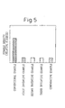
- the pinhole defects in the BOX layer were evaluated by the copper plating method, wherein: each of the samples was arranged so that only the top surface of the substrate touched an electrolyte containing copper ions and the bottom surface of the substrate touched a cathode, and an anode was placed in the electrolyte; then, copper plated portions were made to form on the top surface of the substrate immediately above the portions where pinholes existed in the BOX layer, by applying to the anode and cathode a low voltage of about 10 V which would not destroy the BOX layer; and the density of the pinholes in the BOX layers was evaluated by counting the number of the copper plated portions. Fig.
- FIG. 5 shows the pinhole density in each of the samples of the conventional example, the first to third examples of the present invention and the comparative example. It was made clear that, in the samples of the first to third examples and the comparative example, the pinhole density was reduced to about one fifth that of the sample of the conventional example, and that the number of pinholes decreased as the total amount of the oxygen implantation increased.
- the breakdown electric field of the BOX layer of each sample was evaluated, wherein: the SOI layer of each sample was divided into sections 1 mm 2 each by lithography and etching and an Al electrode was formed on the top surface of each of the sections by vacuum deposition; an Au film was formed on the bottom surface of each sample substrate as the other electrode by vacuum deposition; and the breakdown electric field of the BOX layer was evaluated by applying a voltage to the Al electrodes and the Au electrode on the bottom surface of each substrate, thus imposing an electric field on the BOX layer, and measuring the current flowing at the time.
- the electric field strength was calculated by dividing the voltage imposed on both electrodes by the thickness of the BOX layer.
- Fig. 6 shows the breakdown electric field of the BOX layer in each of the samples of the conventional example, the first to third examples and the comparative example. It is clear in the figure that, in the samples of the first to third examples, the breakdown electric field of the BOX layer is higher than that in the conventional example. It was found out, on the other hand, that, in the sample of the comparative example produced with the same dosing amount as in the first to third examples, the dielectric breakdown characteristic of the BOX layer was inferior to that of the sample of the conventional example. This is presumably because the number of the silicon islands in the BOX layer was increased by simply increasing the dosing amount of the oxygen ions and, as a result, the breakdown electric field decreased, contrary to expectation.
- Fig. 7 shows the density of defects evaluated in terms of etch pit in the SOI layer of each sample. It is clear from the figure that, in the samples of the first to third examples, the defect density is kept at the same level as in the conventional example, despite the fact that they underwent additional ion implantation. The figure also shows that, in the sample of the comparative example, to which the same amount of oxygen ions as in the samples of the first to third examples was implanted in one step, in contrast, the defect density of the SOI layer is higher by more than 10%, which indicates that the damage increases as the amount of the implanted ions increases.
- the present invention makes it possible, in the production of a SIMOX substrate, to obtain a high quality BOX layer whose thickness is heavier than that of a SIMOX substrate produced by a conventional method, by applying to a SIMOX substrate produced by a conventional method additional oxygen implantation so that the peak position of the distribution of implanted oxygen is located at the portion lower than the interface between the BOX layer already formed and the substrate thereunder and, then, a high temperature heat treatment.
Landscapes
- Element Separation (AREA)
Abstract
Description
Claims (13)
- A method of producing a SIMOX substrate wherein a buried oxide layer and a surface silicon layer are formed by applying the implantation of oxygen ions in a silicon substrate and a high temperature heat treatment thereafter, characterized by: forming the buried oxide layer through applying a high temperature heat treatment after an oxygen ion implantation; then applying an additional oxygen ion implantation so that the peak position of the distribution of implanted oxygen is located at a portion lower than the interface between the buried oxide layer, already formed, and the substrate thereunder; and then applying another high temperature heat treatment.
- A method of producing a SIMOX substrate wherein a buried oxide layer and a surface silicon layer are formed by applying the implantation of oxygen ions in a silicon substrate and a high temperature heat treatment thereafter, characterized by: forming the buried oxide layer through applying a high temperature heat treatment after an oxygen ion implantation; then applying an additional oxygen ion implantation so that the dosing amount of the additional oxygen ion implantation does not exceed the total dosing amount of the oxygen ions implanted earlier and that the peak position of the distribution of implanted oxygen is located at a portion lower than the interface between the buried oxide layer, already formed, and the substrate thereunder; and then applying another high temperature heat treatment.
- A method of producing a SIMOX substrate wherein a buried oxide layer and a surface silicon layer are formed by applying the implantation of oxygen ions in a silicon substrate and a high temperature heat treatment thereafter, characterized by: forming the buried oxide layer through applying a high temperature heat treatment after an oxygen ion implantation; then applying an additional oxygen ion implantation so that the accelerating energy formerly applied to the oxygen ion implantation is different from that applied to the additional oxygen ion implantation and that the peak position of the distribution of implanted oxygen is located at a portion lower than the interface between the buried oxide layer, already formed, and the substrate thereunder; and then applying another high temperature heat treatment.
- A method of producing a SIMOX substrate wherein a buried oxide layer and a surface silicon layer are formed by applying the implantation of oxygen ions in a silicon substrate and a high temperature heat treatment thereafter, characterized by: forming the buried oxide layer through applying a high temperature heat treatment after an oxygen ion implantation; then applying an additional oxygen ion implantation so that the dosing amount of the additional oxygen ion implantation does not exceed the total dosing amount of the oxygen ions implanted earlier, that the accelerating energy formerly applied to the oxygen ion implantation is different from that applied to the additional oxygen ion implantation and that the peak position of the distribution of implanted oxygen is located at a portion lower than the interface between the buried oxide layer, already formed, and the substrate thereunder; and then applying another high temperature heat treatment.
- A method of producing a SIMOX substrate wherein a buried oxide layer and a surface silicon layer are formed by applying the implantation of oxygen ions in a silicon substrate and a high temperature heat treatment thereafter, characterized by: forming the buried oxide layer through applying a high temperature heat treatment after an oxygen ion implantation; then partially removing the surface of the surface silicon layer already formed; then applying an additional oxygen ion implantation so that the peak position of the distribution of implanted oxygen is located at a portion lower than the interface between the buried oxide layer, already formed, and the substrate thereunder; and then applying another high temperature heat treatment.
- A method of producing a SIMOX substrate wherein a buried oxide layer and a surface silicon layer are formed by applying the implantation of oxygen ions in a silicon substrate and a high temperature heat treatment thereafter, characterized by: forming the buried oxide layer through applying a high temperature heat treatment after an oxygen ion implantation; then partially removing the surface of the surface silicon layer already formed; then applying an additional oxygen ion implantation so that the dosing amount of the additional oxygen ion implantation does not exceed the total dosing amount of the oxygen ions implanted earlier and that the peak position of the distribution of implanted oxygen is located at a portion lower than the interface between the buried oxide layer, already formed, and the substrate thereunder; and then applying another high temperature heat treatment.
- A method of producing a SIMOX substrate wherein a buried oxide layer and a surface silicon layer are formed by applying the implantation of oxygen ions in a silicon substrate and a high temperature heat treatment thereafter, characterized by: forming the buried oxide layer through applying a high temperature heat treatment after an oxygen ion implantation; then partially removing the surface of the surface silicon layer already formed; then applying an additional oxygen ion implantation so that the accelerating energy formerly applied to the oxygen ion implantation is different from that applied to the additional oxygen ion implantation and that the peak position of the distribution of implanted oxygen is located at a portion lower than the interface between the buried oxide layer, already formed, and the substrate thereunder; and then applying another high temperature heat treatment.
- A method of producing a SIMOX substrate wherein a buried oxide layer and a surface silicon layer are formed by applying the implantation of oxygen ions in a silicon substrate and a high temperature heat treatment thereafter, characterized by: forming the buried oxide layer through applying a high temperature heat treatment after an oxygen ion implantation; then partially removing the surface of the surface silicon layer already formed; then applying an additional oxygen ion implantation so that the dosing amount of the additional oxygen ion implantation does not exceed the total dosing amount of the oxygen ions implanted earlier, that the accelerating energy formerly applied to the oxygen ion implantation is different from that applied to the additional oxygen ion implantation and that the peak position of the distribution of implanted oxygen is located at a portion lower than the interface between the buried oxide layer, already formed, and the substrate thereunder; and then applying another high temperature heat treatment.
- A method of producing a SIMOX substrate according to claim 5, characterized in that the method of removing the surface of the surface silicon layer is any one of etching using a reactive substance, the removal of an oxide layer after forming it by oxidizing the silicon at the surface of the substrate, and surface polishing.
- A method of producing a SIMOX substrate according to claim 6, characterized in that the method of removing the surface of the surface silicon layer is any one of etching using a reactive substance, the removal of an oxide layer after forming it by oxidizing the silicon at the surface of the substrate, and surface polishing.
- A method of producing a SIMOX substrate according to claim 7, characterized in that the method of removing the surface of the surface silicon layer is any one of etching using a reactive substance, the removal of an oxide layer after forming it by oxidizing the silicon at the surface of the substrate, and surface polishing.
- A method of producing a SIMOX substrate according to claim 8, characterized in that the method of removing the surface of the surface silicon layer is any one of etching using a reactive substance, the removal of an oxide layer after forming it by oxidizing the silicon at the surface of the substrate, and surface polishing.
- A SIMOX substrate produced by the production method according to any one of claims 1 to 12, characterized in that the thickness of the surface silicon layer of the SIMOX substrate is 10 to 400 nm, and the thickness of the buried oxide layer thereof is 60 to 250 nm.
Applications Claiming Priority (3)
| Application Number | Priority Date | Filing Date | Title |
|---|---|---|---|
| JP2001093227A JP2002289552A (en) | 2001-03-28 | 2001-03-28 | SIMOX substrate manufacturing method and SIMOX substrate |
| JP2001093227 | 2001-03-28 | ||
| PCT/JP2002/003127 WO2002080276A1 (en) | 2001-03-28 | 2002-03-28 | Production method for simox substrate and simox substrate |
Publications (3)
| Publication Number | Publication Date |
|---|---|
| EP1376699A1 true EP1376699A1 (en) | 2004-01-02 |
| EP1376699A4 EP1376699A4 (en) | 2009-04-08 |
| EP1376699B1 EP1376699B1 (en) | 2012-03-21 |
Family
ID=18947588
Family Applications (1)
| Application Number | Title | Priority Date | Filing Date |
|---|---|---|---|
| EP02707233A Expired - Lifetime EP1376699B1 (en) | 2001-03-28 | 2002-03-28 | Production method for simox substrate and simox substrate |
Country Status (6)
| Country | Link |
|---|---|
| US (1) | US7067402B2 (en) |
| EP (1) | EP1376699B1 (en) |
| JP (1) | JP2002289552A (en) |
| KR (1) | KR100664000B1 (en) |
| TW (1) | TW540105B (en) |
| WO (1) | WO2002080276A1 (en) |
Families Citing this family (22)
| Publication number | Priority date | Publication date | Assignee | Title |
|---|---|---|---|---|
| JP2004119943A (en) * | 2002-09-30 | 2004-04-15 | Renesas Technology Corp | Semiconductor wafer and method of manufacturing the same |
| CN100472001C (en) * | 2003-02-25 | 2009-03-25 | 株式会社上睦可 | Silicon wafer, SOI substrate, silicon single crystal growth method, silicon wafer manufacturing method and SOI substrate manufacturing method |
| JP4790211B2 (en) * | 2003-06-13 | 2011-10-12 | シルトロニック・ジャパン株式会社 | SOI substrate, semiconductor substrate and manufacturing method thereof |
| US8450806B2 (en) | 2004-03-31 | 2013-05-28 | International Business Machines Corporation | Method for fabricating strained silicon-on-insulator structures and strained silicon-on insulator structures formed thereby |
| US20060105559A1 (en) * | 2004-11-15 | 2006-05-18 | International Business Machines Corporation | Ultrathin buried insulators in Si or Si-containing material |
| JP2007005563A (en) * | 2005-06-23 | 2007-01-11 | Sumco Corp | SIMOX wafer manufacturing method |
| US7880204B2 (en) * | 2006-10-02 | 2011-02-01 | Massachusetts Institute Of Technology | System and method for providing a high frequency response silicon photodetector |
| US8110890B2 (en) | 2007-06-05 | 2012-02-07 | Taiwan Semiconductor Manufacturing Company, Ltd. | Method of fabricating semiconductor device isolation structure |
| US8022487B2 (en) * | 2008-04-29 | 2011-09-20 | Intel Corporation | Increasing body dopant uniformity in multi-gate transistor devices |
| JP2010027959A (en) * | 2008-07-23 | 2010-02-04 | Sumco Corp | Method for manufacturing high-resistance simox wafer |
| JP2010118382A (en) * | 2008-11-11 | 2010-05-27 | Sumco Corp | Method of reducing crystal defect of simox wafer |
| JP2010062503A (en) * | 2008-09-08 | 2010-03-18 | Sumco Corp | Method for reducing crystal defect of simox wafer and simox wafer |
| US8030183B2 (en) * | 2008-09-08 | 2011-10-04 | Sumco Corporation | Method for reducing crystal defect of SIMOX wafer and SIMOX wafer |
| JP2010135538A (en) * | 2008-12-04 | 2010-06-17 | Sumco Corp | Method of manufacturing bonded wafer |
| US20100193879A1 (en) * | 2009-02-05 | 2010-08-05 | Ming-Han Liao | Isolation Region Implant and Structure |
| US8168507B2 (en) | 2009-08-21 | 2012-05-01 | International Business Machines Corporation | Structure and method of forming enhanced array device isolation for implanted plate EDRAM |
| JPWO2011118205A1 (en) * | 2010-03-26 | 2013-07-04 | 株式会社Sumco | Manufacturing method of SOI wafer |
| CN102244029A (en) * | 2011-06-28 | 2011-11-16 | 上海宏力半导体制造有限公司 | Manufacturing process of silicon-on-insulator substrate and manufacturing process of silicon-on-insulator device |
| CN102244080A (en) * | 2011-06-28 | 2011-11-16 | 上海宏力半导体制造有限公司 | Silicon-on-insulator (SOI) substrate structure and device |
| CN102522362B (en) * | 2011-12-14 | 2015-06-24 | 中国科学院微电子研究所 | A Method for Improving the Anti-irradiation Performance of SOI Structure |
| CN106783725B (en) * | 2016-12-27 | 2019-09-17 | 上海新傲科技股份有限公司 | The preparation method of substrate with insulating buried layer |
| US11721554B2 (en) * | 2019-03-18 | 2023-08-08 | Intel Corporation | Stress compensation for wafer to wafer bonding |
Family Cites Families (19)
| Publication number | Priority date | Publication date | Assignee | Title |
|---|---|---|---|---|
| US4786608A (en) * | 1986-12-30 | 1988-11-22 | Harris Corp. | Technique for forming electric field shielding layer in oxygen-implanted silicon substrate |
| FR2616590B1 (en) | 1987-06-15 | 1990-03-02 | Commissariat Energie Atomique | METHOD FOR MANUFACTURING AN INSULATOR LAYER BURIED IN A SEMICONDUCTOR SUBSTRATE BY ION IMPLANTATION AND SEMICONDUCTOR STRUCTURE COMPRISING THIS LAYER |
| JPH01117444A (en) | 1987-10-29 | 1989-05-10 | Nec Corp | Supervision control system |
| JP2838444B2 (en) * | 1991-02-05 | 1998-12-16 | 三菱電機株式会社 | Method of forming buried insulating film in silicon substrate |
| JP3291510B2 (en) | 1992-03-31 | 2002-06-10 | シャープ株式会社 | Semiconductor device |
| JPH05291543A (en) | 1992-04-15 | 1993-11-05 | Fujitsu Ltd | Manufacture of semiconductor device |
| JP3139904B2 (en) * | 1993-12-28 | 2001-03-05 | 新日本製鐵株式会社 | Method and apparatus for manufacturing semiconductor substrate |
| JP3036619B2 (en) | 1994-03-23 | 2000-04-24 | コマツ電子金属株式会社 | SOI substrate manufacturing method and SOI substrate |
| JPH07335847A (en) * | 1994-06-14 | 1995-12-22 | Nippon Steel Corp | Method for manufacturing silicon substrate having buried oxide film |
| US6043166A (en) * | 1996-12-03 | 2000-03-28 | International Business Machines Corporation | Silicon-on-insulator substrates using low dose implantation |
| US6069054A (en) * | 1997-12-23 | 2000-05-30 | Integrated Device Technology, Inc. | Method for forming isolation regions subsequent to gate formation and structure thereof |
| JP3762144B2 (en) * | 1998-06-18 | 2006-04-05 | キヤノン株式会社 | Method for manufacturing SOI substrate |
| JP2000082679A (en) * | 1998-07-08 | 2000-03-21 | Canon Inc | Semiconductor substrate and manufacturing method thereof |
| JP3211233B2 (en) | 1998-08-31 | 2001-09-25 | 日本電気株式会社 | SOI substrate and manufacturing method thereof |
| US6180487B1 (en) * | 1999-10-25 | 2001-01-30 | Advanced Micro Devices, Inc. | Selective thinning of barrier oxide through masked SIMOX implant |
| US6461933B2 (en) * | 2000-12-30 | 2002-10-08 | Texas Instruments Incorporated | SPIMOX/SIMOX combination with ITOX option |
| JP2002231651A (en) * | 2001-02-02 | 2002-08-16 | Nippon Steel Corp | SIMOX substrate and method of manufacturing the same |
| US6541356B2 (en) * | 2001-05-21 | 2003-04-01 | International Business Machines Corporation | Ultimate SIMOX |
| US6737332B1 (en) * | 2002-03-28 | 2004-05-18 | Advanced Micro Devices, Inc. | Semiconductor device formed over a multiple thickness buried oxide layer, and methods of making same |
-
2001
- 2001-03-28 JP JP2001093227A patent/JP2002289552A/en active Pending
-
2002
- 2002-03-28 KR KR1020037012632A patent/KR100664000B1/en not_active Expired - Fee Related
- 2002-03-28 WO PCT/JP2002/003127 patent/WO2002080276A1/en not_active Ceased
- 2002-03-28 US US10/473,692 patent/US7067402B2/en not_active Expired - Lifetime
- 2002-03-28 EP EP02707233A patent/EP1376699B1/en not_active Expired - Lifetime
- 2002-03-28 TW TW091106213A patent/TW540105B/en not_active IP Right Cessation
Also Published As
| Publication number | Publication date |
|---|---|
| KR20030089706A (en) | 2003-11-22 |
| JP2002289552A (en) | 2002-10-04 |
| TW540105B (en) | 2003-07-01 |
| US7067402B2 (en) | 2006-06-27 |
| EP1376699A4 (en) | 2009-04-08 |
| KR100664000B1 (en) | 2007-01-03 |
| US20040171228A1 (en) | 2004-09-02 |
| EP1376699B1 (en) | 2012-03-21 |
| WO2002080276A1 (en) | 2002-10-10 |
Similar Documents
| Publication | Publication Date | Title |
|---|---|---|
| EP1376699B1 (en) | Production method for simox substrate and simox substrate | |
| US5436175A (en) | Shallow SIMOX processing method using molecular ion implantation | |
| KR100779341B1 (en) | Process for producing high resistance silicon wafer, and process for producing epitaxial wafer and soi wafer | |
| KR20040015282A (en) | Film or layer made of semi-conductive material and method for producing said film or layer | |
| KR100947815B1 (en) | Manufacturing Method of SOI Wafer and SOI Wafer | |
| WO1999039380A1 (en) | Soi substrate and method for manufacturing the same | |
| KR100765860B1 (en) | Simox substrate and method for production thereof | |
| KR100260574B1 (en) | Manufacturing method of soi substrate | |
| JP3556407B2 (en) | Method for manufacturing semiconductor device | |
| JP2003289051A (en) | SIMOX substrate and method of manufacturing the same | |
| US20020098664A1 (en) | Method of producing SOI materials | |
| US8338277B2 (en) | Method for manufacturing SOI substrate | |
| KR100580998B1 (en) | SOI wafer manufacturing method | |
| JP3996732B2 (en) | SIMOX substrate and manufacturing method thereof | |
| JPS62132344A (en) | Manufacture of silicon substrate for integrated circuit | |
| JP2002231651A (en) | SIMOX substrate and method of manufacturing the same | |
| JP2001257329A (en) | SIMOX substrate and method of manufacturing the same | |
| US20130012008A1 (en) | Method of producing soi wafer | |
| JPH05299349A (en) | Method for manufacturing SOI substrate | |
| JP2002289819A (en) | SIMOX substrate | |
| JP2000068489A (en) | SOI substrate and method of manufacturing the same | |
| JP2008159868A (en) | Method for manufacturing simox substrate | |
| JP2025030418A (en) | SOI WAFER AND ITS MANUFACTURING METHOD | |
| JPH1079356A (en) | Manufacture of semiconductor substrate | |
| JPH11220019A (en) | SOI substrate and manufacturing method thereof |
Legal Events
| Date | Code | Title | Description |
|---|---|---|---|
| PUAI | Public reference made under article 153(3) epc to a published international application that has entered the european phase |
Free format text: ORIGINAL CODE: 0009012 |
|
| 17P | Request for examination filed |
Effective date: 20031008 |
|
| AK | Designated contracting states |
Kind code of ref document: A1 Designated state(s): AT BE CH CY DE DK ES FI FR GB GR IE IT LI LU MC NL PT SE TR |
|
| A4 | Supplementary search report drawn up and despatched |
Effective date: 20090309 |
|
| 17Q | First examination report despatched |
Effective date: 20090730 |
|
| GRAP | Despatch of communication of intention to grant a patent |
Free format text: ORIGINAL CODE: EPIDOSNIGR1 |
|
| GRAS | Grant fee paid |
Free format text: ORIGINAL CODE: EPIDOSNIGR3 |
|
| RAP1 | Party data changed (applicant data changed or rights of an application transferred) |
Owner name: NIPPON STEEL CORPORATION |
|
| GRAA | (expected) grant |
Free format text: ORIGINAL CODE: 0009210 |
|
| AK | Designated contracting states |
Kind code of ref document: B1 Designated state(s): DE FR IT |
|
| REG | Reference to a national code |
Ref country code: DE Ref legal event code: R096 Ref document number: 60242443 Country of ref document: DE Effective date: 20120524 |
|
| RAP2 | Party data changed (patent owner data changed or rights of a patent transferred) |
Owner name: NIPPON STEEL & SUMITOMO METAL CORPORATION |
|
| PLBE | No opposition filed within time limit |
Free format text: ORIGINAL CODE: 0009261 |
|
| STAA | Information on the status of an ep patent application or granted ep patent |
Free format text: STATUS: NO OPPOSITION FILED WITHIN TIME LIMIT |
|
| 26N | No opposition filed |
Effective date: 20130102 |
|
| REG | Reference to a national code |
Ref country code: DE Ref legal event code: R082 Ref document number: 60242443 Country of ref document: DE Representative=s name: VOSSIUS & PARTNER, DE Effective date: 20130227 Ref country code: DE Ref legal event code: R081 Ref document number: 60242443 Country of ref document: DE Owner name: NIPPON STEEL & SUMITOMO METAL CORPORATION, JP Free format text: FORMER OWNER: NIPPON STEEL CORP., TOKIO/TOKYO, JP Effective date: 20120330 Ref country code: DE Ref legal event code: R097 Ref document number: 60242443 Country of ref document: DE Effective date: 20130102 Ref country code: DE Ref legal event code: R081 Ref document number: 60242443 Country of ref document: DE Owner name: NIPPON STEEL & SUMITOMO METAL CORPORATION, JP Free format text: FORMER OWNER: NIPPON STEEL CORPORATION, TOKIO/TOKYO, JP Effective date: 20130227 Ref country code: DE Ref legal event code: R082 Ref document number: 60242443 Country of ref document: DE Representative=s name: VOSSIUS & PARTNER PATENTANWAELTE RECHTSANWAELT, DE Effective date: 20130227 |
|
| REG | Reference to a national code |
Ref country code: FR Ref legal event code: PLFP Year of fee payment: 15 |
|
| REG | Reference to a national code |
Ref country code: FR Ref legal event code: PLFP Year of fee payment: 16 |
|
| REG | Reference to a national code |
Ref country code: FR Ref legal event code: PLFP Year of fee payment: 17 |
|
| PGFP | Annual fee paid to national office [announced via postgrant information from national office to epo] |
Ref country code: IT Payment date: 20190326 Year of fee payment: 18 Ref country code: DE Payment date: 20190312 Year of fee payment: 18 |
|
| PGFP | Annual fee paid to national office [announced via postgrant information from national office to epo] |
Ref country code: FR Payment date: 20190213 Year of fee payment: 18 |
|
| REG | Reference to a national code |
Ref country code: DE Ref legal event code: R082 Ref document number: 60242443 Country of ref document: DE Representative=s name: VOSSIUS & PARTNER PATENTANWAELTE RECHTSANWAELT, DE Ref country code: DE Ref legal event code: R081 Ref document number: 60242443 Country of ref document: DE Owner name: NIPPON STEEL CORPORATION, JP Free format text: FORMER OWNER: NIPPON STEEL & SUMITOMO METAL CORPORATION, TOKYO, JP |
|
| REG | Reference to a national code |
Ref country code: DE Ref legal event code: R119 Ref document number: 60242443 Country of ref document: DE |
|
| PG25 | Lapsed in a contracting state [announced via postgrant information from national office to epo] |
Ref country code: FR Free format text: LAPSE BECAUSE OF NON-PAYMENT OF DUE FEES Effective date: 20200331 Ref country code: DE Free format text: LAPSE BECAUSE OF NON-PAYMENT OF DUE FEES Effective date: 20201001 |
|
| PG25 | Lapsed in a contracting state [announced via postgrant information from national office to epo] |
Ref country code: IT Free format text: LAPSE BECAUSE OF NON-PAYMENT OF DUE FEES Effective date: 20200328 |