EP1376668A1 - Microwave plasma process device, plasma ignition method, plasma forming method, and plasma process method - Google Patents
Microwave plasma process device, plasma ignition method, plasma forming method, and plasma process method Download PDFInfo
- Publication number
- EP1376668A1 EP1376668A1 EP02707230A EP02707230A EP1376668A1 EP 1376668 A1 EP1376668 A1 EP 1376668A1 EP 02707230 A EP02707230 A EP 02707230A EP 02707230 A EP02707230 A EP 02707230A EP 1376668 A1 EP1376668 A1 EP 1376668A1
- Authority
- EP
- European Patent Office
- Prior art keywords
- plasma
- microwave
- space
- processing
- gas
- Prior art date
- Legal status (The legal status is an assumption and is not a legal conclusion. Google has not performed a legal analysis and makes no representation as to the accuracy of the status listed.)
- Granted
Links
Images



Classifications
-
- H—ELECTRICITY
- H01—ELECTRIC ELEMENTS
- H01J—ELECTRIC DISCHARGE TUBES OR DISCHARGE LAMPS
- H01J37/00—Discharge tubes with provision for introducing objects or material to be exposed to the discharge, e.g. for the purpose of examination or processing thereof
- H01J37/32—Gas-filled discharge tubes
- H01J37/32009—Arrangements for generation of plasma specially adapted for examination or treatment of objects, e.g. plasma sources
- H01J37/32192—Microwave generated discharge
-
- H—ELECTRICITY
- H05—ELECTRIC TECHNIQUES NOT OTHERWISE PROVIDED FOR
- H05H—PLASMA TECHNIQUE; PRODUCTION OF ACCELERATED ELECTRICALLY-CHARGED PARTICLES OR OF NEUTRONS; PRODUCTION OR ACCELERATION OF NEUTRAL MOLECULAR OR ATOMIC BEAMS
- H05H1/00—Generating plasma; Handling plasma
- H05H1/24—Generating plasma
- H05H1/46—Generating plasma using applied electromagnetic fields, e.g. high frequency or microwave energy
-
- C—CHEMISTRY; METALLURGY
- C23—COATING METALLIC MATERIAL; COATING MATERIAL WITH METALLIC MATERIAL; CHEMICAL SURFACE TREATMENT; DIFFUSION TREATMENT OF METALLIC MATERIAL; COATING BY VACUUM EVAPORATION, BY SPUTTERING, BY ION IMPLANTATION OR BY CHEMICAL VAPOUR DEPOSITION, IN GENERAL; INHIBITING CORROSION OF METALLIC MATERIAL OR INCRUSTATION IN GENERAL
- C23C—COATING METALLIC MATERIAL; COATING MATERIAL WITH METALLIC MATERIAL; SURFACE TREATMENT OF METALLIC MATERIAL BY DIFFUSION INTO THE SURFACE, BY CHEMICAL CONVERSION OR SUBSTITUTION; COATING BY VACUUM EVAPORATION, BY SPUTTERING, BY ION IMPLANTATION OR BY CHEMICAL VAPOUR DEPOSITION, IN GENERAL
- C23C16/00—Chemical coating by decomposition of gaseous compounds, without leaving reaction products of surface material in the coating, i.e. chemical vapour deposition [CVD] processes
- C23C16/44—Chemical coating by decomposition of gaseous compounds, without leaving reaction products of surface material in the coating, i.e. chemical vapour deposition [CVD] processes characterised by the method of coating
- C23C16/50—Chemical coating by decomposition of gaseous compounds, without leaving reaction products of surface material in the coating, i.e. chemical vapour deposition [CVD] processes characterised by the method of coating using electric discharges
- C23C16/517—Chemical coating by decomposition of gaseous compounds, without leaving reaction products of surface material in the coating, i.e. chemical vapour deposition [CVD] processes characterised by the method of coating using electric discharges using a combination of discharges covered by two or more of groups C23C16/503 - C23C16/515
-
- H—ELECTRICITY
- H01—ELECTRIC ELEMENTS
- H01J—ELECTRIC DISCHARGE TUBES OR DISCHARGE LAMPS
- H01J37/00—Discharge tubes with provision for introducing objects or material to be exposed to the discharge, e.g. for the purpose of examination or processing thereof
- H01J37/32—Gas-filled discharge tubes
- H01J37/32009—Arrangements for generation of plasma specially adapted for examination or treatment of objects, e.g. plasma sources
-
- H—ELECTRICITY
- H01—ELECTRIC ELEMENTS
- H01J—ELECTRIC DISCHARGE TUBES OR DISCHARGE LAMPS
- H01J37/00—Discharge tubes with provision for introducing objects or material to be exposed to the discharge, e.g. for the purpose of examination or processing thereof
- H01J37/32—Gas-filled discharge tubes
- H01J37/32009—Arrangements for generation of plasma specially adapted for examination or treatment of objects, e.g. plasma sources
- H01J37/32321—Discharge generated by other radiation
- H01J37/32339—Discharge generated by other radiation using electromagnetic radiation
Definitions
- the present invention generally relates to a plasma processing apparatus, and particularly, to a plasma processing apparatus that performs plasma processing using plasma excited by a microwave.
- the microwave plasma processing apparatus is attracting attention.
- the plasma potential is relatively low in the microwave plasma processing apparatus, enabling generation of plasma having a low electron temperature and low ion energy.
- the microwave plasma processing apparatus it is possible to prevent metal contamination and ion irradiation damage to a substrate subjected to plasma processing.
- a plasma excitation space can be separated from the plasma processing space, it is possible to carry out plasma processing independent of materials of the substrate and patterns formed on the substrate.
- a gas for exciting plasma (referred to "plasma excitation gas”) is fed into a chamber first, and then the microwave is introduced to the plasma excitation gas to start the generation of plasma (plasma ignition). Because of the high frequency of the microwave, the electrical field of the microwave changes before electrons of the plasma excitation gas are sufficiently accelerated, making plasma ignition difficult. Additionally, in recent plasma processing, a pressure of the plasma excitation gas as low as, for example, 67 Pa (about 0.5 Torr) is sometimes required. Because of the low pressure, the density of the plasma excitation gas is low, further making plasma ignition difficult.
- plasma excitation gas a gas for exciting plasma
- the microwave is emitted from a microwave antenna, and there is no electrical field applied to the substrate to be processed, therefore, free electron emission or other phenomena causing plasma ignition do not occur, making plasma ignition more difficult.
- the pressure inside the processing chamber is set high at the time of plasma ignition, for example, the pressure is set to 133 Pa (about 1 Torr) so as to induce plasma ignition easily; after the ignition, the pressure is lowered to, for example, 7 Pa (about 50 mTorr).
- this plasma ignition an additional control procedure not relevant to the object plasma processing has to be gone through to increase the pressure inside the processing chamber for plasma ignition and to lower the pressure after the plasma ignition, and this lengthens the preparation time before plasma processing starts, and lowers throughput.
- a general object of the present invention is to provide a novel and useful microwave plasma processing apparatus, a plasma ignition method, a plasma forming method, and a plasma processing method able to solve one or more problems of the related art.
- a more specific object of the present invention is to provide a microwave plasma processing apparatus, a plasma ignition method, a plasma forming method, and a plasma processing method enabling fast and easy plasma ignition at a pressure for plasma processing.
- a microwave plasma processing apparatus that generates plasma by a microwave and carries out plasma processing, comprising a plasma ignition facilitating unit configured to facilitate plasma ignition by the microwave.
- a method of inducing plasma ignition by a microwave comprising the steps of: evacuating a processing chamber to a predetermined vacuum; supplying a plasma excitation gas to the processing chamber; emitting at least one of vacuum ultraviolet rays, X-rays, a laser beam, an electron beam, and light from an excimer lamp to the plasma excitation gas inside the processing chamber; and introducing the microwave to the plasma excitation gas in the processing chamber to induce plasma ignition.
- a method of forming plasma by radiating a microwave from a microwave antenna comprising the steps of: evacuating a processing chamber to a predetermined vacuum; supplying a plasma excitation gas to the processing chamber; emitting vacuum ultraviolet rays to the plasma excitation gas inside the processing chamber through a transmission window mounted on the processing chamber; focusing, by the transmission window, the vacuum ultraviolet rays to a predetermined position; ionizing at least a part of the plasma excitation gas; and radiating the microwave into the processing chamber to induce plasma ignition.
- a plasma processing method for processing a substrate using plasma formed by radiating a microwave from a microwave antenna comprising the steps of: evacuating a processing chamber to a predetermined vacuum; supplying a plasma excitation gas to the processing chamber; emitting vacuum ultraviolet rays to the plasma excitation gas inside the processing chamber through a transmission window mounted on the processing chamber; focusing, by the transmission window, the vacuum ultraviolet rays to a predetermined position; ionizing at least part of the plasma excitation gas; radiating the microwave into the processing chamber to induce plasma ignition; and feeding a process gas for processing the substrate into the processing chamber after the plasma ignition.
- a plasma ignition facilitating unit is provided to facilitate plasma ignition induced by a microwave, it is possible to induce plasma ignition easily and quickly with only the microwave, even under conditions not favorable to plasma ignition.
- the plasma ignition facilitating unit may have a configuration in which vacuum ultraviolet rays, X-rays, a laser beam, an electron beam, or light from an excimer lamp is emitted to a plasma excitation space to induce plasma ignition easily.
- vacuum ultraviolet rays emitted from a deuterium lamp for example, vacuum ultraviolet rays at a wavelength of 135 nm, to penetrate a transmission window and irradiate the plasma excitation space in the processing chamber.
- the plasma excitation gas in the plasma excitation space is ionized by the vacuum ultraviolet rays to serve as seeds for generating plasma.
- a microwave it is possible to generate plasma easily.
- FIG. 1 is a schematic view showing a configuration of a microwave plasma processing apparatus according to an embodiment of the present invention.
- the microwave plasma processing apparatus 10 includes a processing chamber 12, a slot antenna (microwave antenna) 14 above the processing chamber 12, a dielectric separation wall 16 below the slot antenna 14, a plasma excitation gas shower plate 18 below the dielectric separation wall 16 for feeding a plasma excitation gas, a process gas shower plate 20 below the plasma excitation gas shower plate 18 for feeding a process gas, a stand 22 below the process gas shower plate 20, and a magnetron 24 for generating a microwave.
- a slot antenna microwave antenna
- the microwave generated by the magnetron 24, for example, at 2.45 GHz, is directed to the slot antenna 14 through a wave guide (not illustrated).
- the microwave directed to the slot antenna 14 passes through the dielectric separation wall 16 and the plasma excitation gas shower plate 18, and is directed to a plasma excitation space 26.
- a plasma excitation gas for example, any noble gas of Argon (Ar), Krypton (Kr), and Xenon (Xe), comes out from the plasma excitation gas shower plate 18 and enters the plasma excitation space 26, where the plasma excitation gas is excited by the microwave and plasma is generated.
- a process gas is supplied to the processing space 28.
- a semiconductor wafer W such as a silicon wafer, is located to be subjected to plasma processing in the process gas and the plasma.
- the resulting gas of the plasma processing is exhausted by a not illustrated pump through an exhaust port 12a provided at the bottom of the processing chamber 12.
- microwave ignition is induced by the introduced microwave in the plasma excitation space 26.
- a plasma ignition facilitating unit is provided to assist or facilitate plasma ignition induced by the microwave.
- the plasma ignition facilitating unit of the present embodiment includes a deuterium lamp 30 mounted on a side wall of the processing chamber 12 that defines the plasma excitation space 26 and a transmission window 32.
- the deuterium lamp 30 emits vacuum ultraviolet rays at a wavelength of 135 nm.
- the vacuum ultraviolet rays pass through the transmission window 32 and are directed to the plasma excitation space 26, where the vacuum ultraviolet rays induce ionization of the plasma excitation gas, and thereby facilitate microwave plasma ignition.
- the transmission window 32 be made from CaF 2 , MgF 2 , LiF and so on so that the vacuum ultraviolet rays at short wavelengths are not absorbed.
- the vacuum ultraviolet rays have a very good ionization efficiency at a pressure around a range from 1.34 Pa (about 0.01 Torr) to 13.4 Pa (about 0.1 Torr), it is preferable to use the vacuum ultraviolet rays in the plasma ignition facilitating unit in the present embodiment.
- the vacuum ultraviolet rays emitted from the deuterium lamp 30 have short wavelengths and thus high energy, they can efficiently ionize the plasma excitation gas constituted by a noble gas.
- Krypton (Kr) gas can be used as the plasma excitation gas.
- the energy necessary to remove an electron from a Krypton atom is 13.8 eV.
- the energy of a photon of the vacuum ultraviolet rays at a wavelength of 135 nm is 9 eV. Therefore, the Krypton atom receives 18 eV if two such photons are absorbed, making it possible to remove an electron from the Krypton atom.
- the transmission window 32 be made into a convex lens to focus the vacuum ultraviolet rays to a specified position in the plasma excitation space 26.
- the focusing position (P) of the vacuum ultraviolet rays is one of the positions where the electric field of the microwave is strongest, for example, at nodes of a stationary wave of the microwave or middle points between two nodes (namely, antinodes of the stationary wave) in the plasma excitation space 26.
- the process gas shower plate 20 is made of conductive materials, and the microwave is reflected by the plasma excitation gas shower plate 18 and the process gas shower plate 20, thereby, the stationary wave of the microwave is to generated between the plasma excitation gas shower plate 18 and the process gas shower plate 20. Therefore, in the present embodiment, a convex lens is selected to be used as the transmission window 32 so that its focal point is located at an antinode of the stationary wave. Namely, the distance L from the plasma excitation gas shower plate 18 to the focal point equals to one-fourth of the wave length ⁇ of the microwave ( ⁇ /4).
- the distance L mentioned above is not limited to one-fourth of the wave length ⁇ of the microwave, but it may be other distances corresponding to other positions of the antinodes of the stationary wave, for example, 3 ⁇ /4, 5 ⁇ /4, or n ⁇ /4 (where n is an integer).
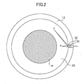
- FIG. 2 is a plan view of the plasma excitation space 26 when the semiconductor wafer W is viewed from the top perpendicularly, showing the focusing position of the transmission window 32.
- the position (P) where the vacuum ultraviolet rays are focused namely, the position of the focusing point of the transmission window 32 (a convex lens)
- the position of the plasma ignition is out of the right cylindrical region with the semiconductor wafer W as a base.
- the plasma ignition takes place above but close to the semiconductor wafer W, it may result in adverse influence on the semiconductor wafer W because the semiconductor wafer W ends up being on the path for propagating the plasma excitation gas.
- the position of the plasma ignition be out of the right cylindrical region with the semiconductor wafer W as a base.
- the process gas shower plate 20 is not illustrated.
- FIG. 3 is a flowchart showing the plasma processing carried out by the microwave plasma processing apparatus 10 of the present embodiment.
- the processing chamber 12 is evacuated to a predetermined vacuum (step 1).
- a plasma excitation gas is supplied to the plasma excitation space 26 (step 2).
- the deuterium lamp 30 emits vacuum ultraviolet rays, and the vacuum ultraviolet rays pass through the transmission window 32 and are directed to the plasma excitation space 26 (step 3).
- the vacuum ultraviolet rays remove electrons from atoms of the plasma excitation gas, and in this state, a microwave is introduced to the plasma excitation space 26 from the slot antenna 14 to induce plasma ignition (step 4).
- plasma ignition is induced, plasma is generated continuously from then on. The thus generated plasma passes through the openings in the process gas shower plate 20, and enters the processing space 28.
- plasma processing is carried out on the semiconductor wafer W (step 5).
- At least one of O 2 , NH 3 , N 2 , and H 2 may be used as the process gas and supplied to the processing space 28 from the process gas shower plate 20.
- fluorocarbon or halogen gas may be used as the process gas and supplied to the processing space 28 from the process gas shower plate 20.
- the process gas is supplied from the process gas shower plate 20 to the processing space 28, which is separated from the plasma excitation space 26, and flows from the wafer W toward the exhaust port 12a provided at the bottom of the processing chamber 12. That is, the process gas cannot enter into the plasma excitation space 26. Therefore, at the time of plasma ignition, the process gas does not exist in the plasma excitation space 26, and this prevents problems caused by dissociation of the process gas at the time of plasma ignition.
- the deuterium lamp 30 and the transmission window 32 are mounted on the side wall of the processing chamber 12, but they can also be mounted at different positions.
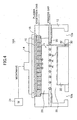
- FIG. 4 is a schematic view showing a configuration of a modification to the microwave plasma processing apparatus shown in FIG. 1.
- the deuterium lamp 30 and the transmission window 32 are mounted on the bottom of the processing chamber 12.
- the walls defining the plasma excitation space 26 are smooth, it is possible to prevent abnormal microwave discharge caused by a discontinuity of the walls defining the plasma excitation space 26.
- FIG. 5 is a schematic view showing a configuration of another modification to the microwave plasma processing apparatus shown in FIG. 1.
- the deuterium lamp 30 is mounted on the outer side of the processing chamber 12, and the space between the deuterium lamp 30 and the transmission window 32 (the space that the vacuum ultraviolet rays pass through) is maintained to be in a vacuum, because otherwise the 135 nm vacuum ultraviolet rays emitted from the deuterium lamp 30 are absorbed in the air.
- the space between the deuterium lamp 30 and the transmission window 32 may be filled with a helium gas.
- the deuterium lamp 30 may have a reflector to condense the vacuum ultraviolet rays emitted from the deuterium lamp 30 in various directions. In this case, it is not necessary to make the transmission window 32 a convex lens; for example, a planar transmission window 32 is sufficient.
- the plasma ignition facilitating unit is configured to emit the vacuum ultraviolet rays, but the present invention is not limited to this.
- the present invention is applicable to any other configuration provided that ionization of the plasma excitation gas is enabled.
- the vacuum ultraviolet rays instead of the vacuum ultraviolet rays, X-rays, a laser beam, an electron beam, or light from an excimer lamp may be used to ionize the plasma excitation gas.
- a plasma ignition facilitating unit is provided to facilitate plasma ignition induced by a microwave, it is possible to induce plasma ignition easily and quickly with the microwave only, even under conditions not favorable to plasma ignition.
- the plasma ignition facilitating unit may have a configuration in which the vacuum ultraviolet rays from a deuterium lamp penetrate a transmission window and irradiate a plasma excitation space in a processing chamber; thereby, it is possible to facilitate plasma ignition with a simple configuration.
Landscapes
- Chemical & Material Sciences (AREA)
- Physics & Mathematics (AREA)
- Engineering & Computer Science (AREA)
- Plasma & Fusion (AREA)
- Analytical Chemistry (AREA)
- Electromagnetism (AREA)
- Toxicology (AREA)
- Health & Medical Sciences (AREA)
- General Chemical & Material Sciences (AREA)
- Chemical Kinetics & Catalysis (AREA)
- Materials Engineering (AREA)
- Mechanical Engineering (AREA)
- Metallurgy (AREA)
- Organic Chemistry (AREA)
- Spectroscopy & Molecular Physics (AREA)
- Drying Of Semiconductors (AREA)
- Plasma Technology (AREA)
- Physical Or Chemical Processes And Apparatus (AREA)
- Chemical Vapour Deposition (AREA)
Abstract
Description
Claims (23)
- A microwave plasma processing apparatus that generates plasma by a microwave and carries out plasma processing, comprising:a plasma ignition facilitating unit configured to facilitate plasma ignition by the microwave.
- The microwave plasma processing apparatus according to claim 1, wherein the microwave used for generation of the plasma is directed into a processing chamber from a microwave antenna through a microwave transmission window that is a part of the processing chamber.
- The microwave plasma processing apparatus according to claim 1, wherein the plasma ignition facilitating unit emits at least one of vacuum ultraviolet rays, X-rays, a laser beam, an electron beam, and light from an excimer lamp to a plasma excitation space to induce the plasma ignition.
- The microwave plasma processing apparatus according to claim 3, wherein the plasma ignition facilitating unit comprises:a deuterium lamp that emits the vacuum ultraviolet rays; anda transmission window that directs the vacuum ultraviolet rays passing therethrough to the plasma excitation space.
- The microwave plasma processing apparatus according to claim 4, wherein a space between the deuterium lamp and the transmission window is maintained to be at a vacuum.
- The microwave plasma processing apparatus according to claim 4, wherein a space between the deuterium lamp and the transmission window is filled with a helium gas.
- The microwave plasma processing apparatus according to claim 4, wherein the deuterium lamp and the transmission window are mounted on side walls of a processing chamber defining the plasma excitation space.
- The microwave plasma processing apparatus according to claim 4, wherein the deuterium lamp and the transmission window are mounted on a bottom of a processing chamber defining the plasma excitation space.
- The microwave plasma processing apparatus according to claim 4, wherein the transmission window includes a convex lens having a focal point at a predetermined position in the plasma excitation space.
- The microwave plasma processing apparatus according to claim 9, wherein the predetermined position is out of a space right above a substrate to be processed.
- The microwave plasma processing apparatus according to claim 9, wherein at the predetermined position, an electric field of the microwave radiated inside the processing chamber is a maximum.
- The microwave plasma processing apparatus according to claim 9, wherein a distance from the predetermined position to a surface of a plasma excitation gas shower plate for feeding the plasma excitation gas into the plasma excitation space is a multiple of λ/4, where λ is the wave length of the microwave.
- The microwave plasma processing apparatus according to claim 4, wherein the transmission window is formed from one of CaF2, MgF2, and LiF.
- The microwave plasma processing apparatus according to claim 3, wherein the plasma excitation space is separated from a processing space by a process gas shower plate, and a process gas is supplied from the process gas shower plate to the processing space thereby preventing the process gas from entering into the plasma excitation space.
- A method of inducing plasma ignition by a microwave, comprising the steps of:evacuating a processing chamber to a predetermined vacuum;supplying a plasma excitation gas to the processing chamber;emitting at least one of vacuum ultraviolet rays, X-rays, a laser beam, an electron beam, and light from an excimer lamp to the plasma excitation gas inside the processing chamber; andintroducing the microwave to the plasma excitation gas in the processing chamber to induce plasma ignition.
- A method of forming plasma by radiating a microwave from a microwave antenna, comprising the steps of:evacuating a processing chamber to a predetermined vacuum;supplying a plasma excitation gas to the processing chamber;emitting vacuum ultraviolet rays to the plasma excitation gas inside the processing chamber through a transmission window mounted on the processing chamber;focusing, by the transmission window, the vacuum ultraviolet rays to a predetermined position;ionizing at least a part of the plasma excitation gas;radiating the microwave into the processing chamber to induce plasma ignition.
- A plasma processing method for processing a substrate using plasma formed by radiating a microwave from a microwave antenna, comprising the steps of:evacuating a processing chamber to a predetermined vacuum;supplying a plasma excitation gas to the evacuated processing chamber;emitting vacuum ultraviolet rays to the plasma excitation gas inside the processing chamber through a transmission window mounted on'the processing chamber;focusing, by the transmission window, the vacuum ultraviolet rays to a predetermined position;ionizing at least a part of the plasma excitation gas;radiating the microwave into the processing chamber to induce plasma ignition; andfeeding a process gas for processing the substrate into the processing chamber after the plasma ignition.
- The plasma processing method according to claim 17, wherein the plasma excitation gas comprises a noble gas including one of Argon (Ar), Krypton (Kr), and Xenon (Xe) .
- The plasma processing method according to claim 17, wherein the process gas includes at least one of O2, NH3, N2, and H2.
- The plasma processing method according to claim 19, wherein the substrate is a silicon wafer, and the process gas is fed into the processing space to form at least one of a silicon dioxide film, a silicon nitride film, and a silicon nitride oxide film on the silicon wafer.
- The plasma processing method according to claim 17, wherein the process gas includes at least one of a fluorocarbon gas and a halogen gas.
- The plasma processing method according to claim 21, wherein the process gas is fed into the processing space to etch the substrate.
- The plasma processing method according to claim 17, wherein the plasma excitation gas is supplied to a plasma excitation space separated from a processing space in which the substrate is located, and the process gas is supplied to the processing space thereby preventing the process gas from entering into the plasma excitation space at the time of plasma ignition.
Applications Claiming Priority (3)
| Application Number | Priority Date | Filing Date | Title |
|---|---|---|---|
| JP2001094277A JP4799748B2 (en) | 2001-03-28 | 2001-03-28 | Microwave plasma process apparatus, plasma ignition method, plasma formation method, and plasma process method |
| JP2001094277 | 2001-03-28 | ||
| PCT/JP2002/003113 WO2002080254A1 (en) | 2001-03-28 | 2002-03-28 | Microwave plasma process device, plasma ignition method, plasma forming method, and plasma process method |
Publications (3)
| Publication Number | Publication Date |
|---|---|
| EP1376668A1 true EP1376668A1 (en) | 2004-01-02 |
| EP1376668A4 EP1376668A4 (en) | 2006-02-15 |
| EP1376668B1 EP1376668B1 (en) | 2007-08-22 |
Family
ID=18948501
Family Applications (1)
| Application Number | Title | Priority Date | Filing Date |
|---|---|---|---|
| EP02707230A Expired - Lifetime EP1376668B1 (en) | 2001-03-28 | 2002-03-28 | Microwave plasma process device, plasma ignition method, plasma forming method, and plasma process method |
Country Status (7)
| Country | Link |
|---|---|
| US (1) | US7141756B2 (en) |
| EP (1) | EP1376668B1 (en) |
| JP (1) | JP4799748B2 (en) |
| KR (1) | KR100573210B1 (en) |
| CN (2) | CN1945800A (en) |
| DE (1) | DE60221975T2 (en) |
| WO (1) | WO2002080254A1 (en) |
Cited By (1)
| Publication number | Priority date | Publication date | Assignee | Title |
|---|---|---|---|---|
| WO2021030342A1 (en) | 2019-08-12 | 2021-02-18 | Mattson Technology, Inc. | Enhanced ignition in inductively coupled plasmas for workpiece processing |
Families Citing this family (32)
| Publication number | Priority date | Publication date | Assignee | Title |
|---|---|---|---|---|
| JP4544447B2 (en) | 2002-11-29 | 2010-09-15 | パナソニック株式会社 | Plasma doping method |
| JP2005175028A (en) * | 2003-12-09 | 2005-06-30 | Canon Inc | Plasma processing method and plasma processing apparatus |
| KR100550342B1 (en) * | 2004-02-24 | 2006-02-08 | 삼성전자주식회사 | A semiconductor substrate processing apparatus comprising a gas spreading method and a shower head and a shower head |
| KR100614648B1 (en) * | 2004-07-15 | 2006-08-23 | 삼성전자주식회사 | Substrate Processing Apparatus Used for Manufacturing Semiconductor Devices |
| US7381291B2 (en) * | 2004-07-29 | 2008-06-03 | Asm Japan K.K. | Dual-chamber plasma processing apparatus |
| WO2006033164A1 (en) * | 2004-09-24 | 2006-03-30 | Tadahiro Ohmi | Organic el light emitting element, manufacturing method thereof and display apparatus |
| JP2006186245A (en) * | 2004-12-28 | 2006-07-13 | Tokyo Electron Ltd | Method of nitriding tunnel oxide film, method of manufacturing nonvolatile memory element, nonvolatile memory element, computer program, and recording medium |
| JP4620537B2 (en) * | 2005-07-21 | 2011-01-26 | 東京エレクトロン株式会社 | Plasma processing apparatus and plasma processing apparatus control method |
| US7579287B2 (en) | 2005-08-12 | 2009-08-25 | Canon Kabushiki Kaisha | Surface treatment method, manufacturing method of semiconductor device, and manufacturing method of capacitive element |
| JP4708998B2 (en) | 2005-12-22 | 2011-06-22 | キヤノン株式会社 | Patterning method, electro-optical device manufacturing method, color filter manufacturing method, luminous body manufacturing method, and thin film transistor manufacturing method |
| KR100864111B1 (en) * | 2006-05-22 | 2008-10-16 | 최대규 | Inductively coupled plasma reactor |
| JP5069427B2 (en) * | 2006-06-13 | 2012-11-07 | 北陸成型工業株式会社 | Shower plate, and plasma processing apparatus, plasma processing method and electronic device manufacturing method using the same |
| JP5651843B2 (en) * | 2007-09-10 | 2015-01-14 | イマジニアリング株式会社 | Measuring method and measuring device |
| KR100963848B1 (en) * | 2007-12-14 | 2010-07-09 | 다이나믹솔라디자인 주식회사 | Capacitively Coupled Plasma Reactor with Multi-Laser Scanning Line |
| KR100979187B1 (en) * | 2007-12-14 | 2010-08-31 | 다이나믹솔라디자인 주식회사 | Dual Plasma Reactor for Dual Substrate Processing with Multi Laser Scanning Lines |
| KR101434145B1 (en) * | 2007-12-27 | 2014-08-26 | 주식회사 뉴파워 프라즈마 | Inductively Coupled Plasma Reactor with Multiple Laser Scanning Lines |
| EP2284869B9 (en) * | 2008-05-26 | 2015-10-21 | Mitsubishi Electric Corporation | Thin film formation device and semiconductor film manufacturing method |
| US20090309623A1 (en) * | 2008-06-11 | 2009-12-17 | Amethyst Research, Inc. | Method for Assessment of Material Defects |
| KR101023645B1 (en) * | 2008-09-02 | 2011-03-22 | 에이피시스템 주식회사 | Apparatus for Light Induced Chemical Vapor Deposition |
| US20100096569A1 (en) * | 2008-10-21 | 2010-04-22 | Applied Materials, Inc. | Ultraviolet-transmitting microwave reflector comprising a micromesh screen |
| KR101096458B1 (en) * | 2009-12-03 | 2011-12-20 | 비아이 이엠티 주식회사 | Process gas separation supply type atmospheric plasma device |
| US9435031B2 (en) | 2014-01-07 | 2016-09-06 | International Business Machines Corporation | Microwave plasma and ultraviolet assisted deposition apparatus and method for material deposition using the same |
| CN103982917B (en) * | 2014-05-04 | 2015-11-25 | 清华大学 | Utilize the controlled multipoint ignition device that electromagnetic wave plasma realizes |
| CN104675597B (en) * | 2015-02-05 | 2016-05-25 | 吉林大学 | Reflection pin formula vehicle-carried microwave reformer plasma ignition device |
| US10244613B2 (en) | 2015-10-04 | 2019-03-26 | Kla-Tencor Corporation | System and method for electrodeless plasma ignition in laser-sustained plasma light source |
| CN109905955B (en) * | 2019-03-13 | 2023-12-22 | 中国科学院微电子研究所 | Atomic plasma formation device and its application |
| EP3908087B1 (en) * | 2019-05-09 | 2024-11-27 | SPP Technologies Co., Ltd. | Plasma ignition method and plasma generation device |
| US11262664B2 (en) | 2019-11-19 | 2022-03-01 | Kla Corporation | System and method for protecting optics from vacuum ultraviolet light |
| US20230207274A1 (en) * | 2020-06-02 | 2023-06-29 | Lam Research Corporation | Photoelectron assisted plasma ignition |
| DE102022000797A1 (en) | 2021-03-10 | 2022-09-15 | Mathias Herrmann | Ignition concept and combustion concept for engines and rockets; the most effective or directed excitation and ignition possible by means of adapted electromagnetic radiation or electromagnetic waves (e.g. radio waves, microwaves, magnetic waves) and catalytic absorbers to increase the energetic efficiency and thrust |
| US20240162011A1 (en) * | 2022-11-15 | 2024-05-16 | Applied Materials, Inc. | Addition of external ultraviolet light for improved plasma strike consistency |
| CN121416388B (en) * | 2025-12-30 | 2026-04-21 | 季华实验室 | Remote plasma source system based on 172nm ultraviolet light-assisted ignition |
Family Cites Families (21)
| Publication number | Priority date | Publication date | Assignee | Title |
|---|---|---|---|---|
| JPS6245122A (en) * | 1985-08-23 | 1987-02-27 | Hitachi Ltd | Treater |
| JPH0782280B2 (en) * | 1986-10-09 | 1995-09-06 | 株式会社リコー | Fixing temperature controller |
| JPH0810635B2 (en) * | 1986-12-19 | 1996-01-31 | 富士通株式会社 | Plasma processing device |
| US4933602A (en) * | 1987-03-11 | 1990-06-12 | Hitachi, Ltd. | Apparatus for generating light by utilizing microwave |
| JPH0831417B2 (en) * | 1988-12-02 | 1996-03-27 | 工業技術院長 | Plasma processing deposition equipment |
| JP3258439B2 (en) * | 1993-04-14 | 2002-02-18 | 株式会社半導体エネルギー研究所 | Gas phase reactor |
| JPH06342768A (en) * | 1993-06-02 | 1994-12-13 | Anelva Corp | Ecr surface treating apparatus and desicharge starting method thereof |
| US5468296A (en) * | 1993-12-17 | 1995-11-21 | Lsi Logic Corporation | Apparatus for igniting low pressure inductively coupled plasma |
| JPH07283140A (en) * | 1994-04-05 | 1995-10-27 | Nippon Telegr & Teleph Corp <Ntt> | Active atom supply control method |
| JP3360097B2 (en) * | 1994-07-06 | 2002-12-24 | 株式会社ニコン | Vacuum ultraviolet optical device |
| DE19532435C2 (en) * | 1995-09-02 | 2001-07-19 | Ver Foerderung Inst Kunststoff | Device and method for generating a plasma |
| JP3150056B2 (en) | 1995-10-19 | 2001-03-26 | 東京エレクトロン株式会社 | Plasma processing equipment |
| JP3897380B2 (en) * | 1996-09-06 | 2007-03-22 | 俊夫 後藤 | Processing method and apparatus |
| US6150628A (en) * | 1997-06-26 | 2000-11-21 | Applied Science And Technology, Inc. | Toroidal low-field reactive gas source |
| JP3432722B2 (en) * | 1997-09-30 | 2003-08-04 | 東京エレクトロン株式会社 | Plasma film forming method and plasma processing apparatus |
| TW385623B (en) * | 1997-10-20 | 2000-03-21 | Sumitomo Metal Ind | Apparatus and method for microwave plasma process |
| JP3161394B2 (en) * | 1997-12-03 | 2001-04-25 | 日本電気株式会社 | Plasma CVD equipment |
| JP4127435B2 (en) * | 1998-10-16 | 2008-07-30 | 後藤 俊夫 | Atomic radical measurement method and apparatus |
| US6263830B1 (en) * | 1999-04-12 | 2001-07-24 | Matrix Integrated Systems, Inc. | Microwave choke for remote plasma generator |
| US20030051990A1 (en) * | 2001-08-15 | 2003-03-20 | Crt Holdings, Inc. | System, method, and apparatus for an intense ultraviolet radiation source |
| US6897615B2 (en) * | 2001-11-01 | 2005-05-24 | Axcelis Technologies, Inc. | Plasma process and apparatus |
-
2001
- 2001-03-28 JP JP2001094277A patent/JP4799748B2/en not_active Expired - Fee Related
-
2002
- 2002-03-28 CN CNA2006100871845A patent/CN1945800A/en active Pending
- 2002-03-28 US US10/473,062 patent/US7141756B2/en not_active Expired - Fee Related
- 2002-03-28 DE DE60221975T patent/DE60221975T2/en not_active Expired - Lifetime
- 2002-03-28 EP EP02707230A patent/EP1376668B1/en not_active Expired - Lifetime
- 2002-03-28 KR KR1020037012475A patent/KR100573210B1/en not_active Expired - Fee Related
- 2002-03-28 WO PCT/JP2002/003113 patent/WO2002080254A1/en not_active Ceased
- 2002-03-28 CN CNB028074890A patent/CN1311531C/en not_active Expired - Fee Related
Cited By (2)
| Publication number | Priority date | Publication date | Assignee | Title |
|---|---|---|---|---|
| WO2021030342A1 (en) | 2019-08-12 | 2021-02-18 | Mattson Technology, Inc. | Enhanced ignition in inductively coupled plasmas for workpiece processing |
| EP4000088A4 (en) * | 2019-08-12 | 2022-09-28 | Mattson Technology, Inc. | ENHANCED IGNITION IN INDUCTION COUPLED PLASMAS FOR WORKPIECE PROCESSING |
Also Published As
| Publication number | Publication date |
|---|---|
| EP1376668B1 (en) | 2007-08-22 |
| US7141756B2 (en) | 2006-11-28 |
| JP2002299241A (en) | 2002-10-11 |
| DE60221975D1 (en) | 2007-10-04 |
| CN1502121A (en) | 2004-06-02 |
| US20040118834A1 (en) | 2004-06-24 |
| EP1376668A4 (en) | 2006-02-15 |
| JP4799748B2 (en) | 2011-10-26 |
| KR20030088117A (en) | 2003-11-17 |
| CN1311531C (en) | 2007-04-18 |
| KR100573210B1 (en) | 2006-04-24 |
| WO2002080254A1 (en) | 2002-10-10 |
| CN1945800A (en) | 2007-04-11 |
| DE60221975T2 (en) | 2008-05-15 |
Similar Documents
| Publication | Publication Date | Title |
|---|---|---|
| US7141756B2 (en) | Microwave plasma processing apparatus, plasma ignition method, plasma forming method, and plasma processing method | |
| US12347677B2 (en) | Enhanced ignition in inductively coupled plasmas for workpiece processing | |
| US6761796B2 (en) | Method and apparatus for micro-jet enabled, low-energy ion generation transport in plasma processing | |
| JP5385875B2 (en) | Plasma processing apparatus and optical monitor apparatus | |
| JP3642809B2 (en) | Low pressure inductively coupled plasma ignition device | |
| EP0919068A1 (en) | Method and apparatus for starting difficult to start electrodeless lamps | |
| US6965117B2 (en) | Extreme UV light source and semiconductor exposure device | |
| KR20000063075A (en) | Method for reducing topography dependent charging effects in a plasma enhanced semiconductor wafer processing system | |
| JP4204689B2 (en) | Laser oscillation apparatus, exposure apparatus, and device manufacturing method | |
| JP2000252565A (en) | Laser oscillation apparatus, exposure apparatus, and device manufacturing method | |
| JPH09145675A (en) | Neutral radical measuring method and neutral radical measuring device | |
| JPH06342768A (en) | Ecr surface treating apparatus and desicharge starting method thereof |
Legal Events
| Date | Code | Title | Description |
|---|---|---|---|
| PUAI | Public reference made under article 153(3) epc to a published international application that has entered the european phase |
Free format text: ORIGINAL CODE: 0009012 |
|
| 17P | Request for examination filed |
Effective date: 20030926 |
|
| AK | Designated contracting states |
Kind code of ref document: A1 Designated state(s): AT BE CH CY DE DK ES FI FR GB GR IE IT LI LU MC NL PT SE TR |
|
| AX | Request for extension of the european patent |
Extension state: AL LT LV MK RO SI |
|
| A4 | Supplementary search report drawn up and despatched |
Effective date: 20060102 |
|
| 17Q | First examination report despatched |
Effective date: 20060227 |
|
| GRAP | Despatch of communication of intention to grant a patent |
Free format text: ORIGINAL CODE: EPIDOSNIGR1 |
|
| GRAS | Grant fee paid |
Free format text: ORIGINAL CODE: EPIDOSNIGR3 |
|
| GRAA | (expected) grant |
Free format text: ORIGINAL CODE: 0009210 |
|
| AK | Designated contracting states |
Kind code of ref document: B1 Designated state(s): DE FR IT |
|
| RBV | Designated contracting states (corrected) |
Designated state(s): DE FR IT |
|
| RIN1 | Information on inventor provided before grant (corrected) |
Inventor name: SUGAWA, SHIGETOSHIDEPT. OF ELECTRONIC ENGIN. GRADU Inventor name: OHMI, TADAHIRO Inventor name: GOTO, TETSUYADEPT. OF ELECTRONIC ENGIN. GRADUATE Inventor name: HIRAYAMA, MASAKIDEPT. OF ELECTRONIC ENGIN. GRADUAT |
|
| REF | Corresponds to: |
Ref document number: 60221975 Country of ref document: DE Date of ref document: 20071004 Kind code of ref document: P |
|
| ET | Fr: translation filed | ||
| PLBE | No opposition filed within time limit |
Free format text: ORIGINAL CODE: 0009261 |
|
| STAA | Information on the status of an ep patent application or granted ep patent |
Free format text: STATUS: NO OPPOSITION FILED WITHIN TIME LIMIT |
|
| 26N | No opposition filed |
Effective date: 20080526 |
|
| PGFP | Annual fee paid to national office [announced via postgrant information from national office to epo] |
Ref country code: FR Payment date: 20120319 Year of fee payment: 11 |
|
| PGFP | Annual fee paid to national office [announced via postgrant information from national office to epo] |
Ref country code: IT Payment date: 20120321 Year of fee payment: 11 |
|
| PGFP | Annual fee paid to national office [announced via postgrant information from national office to epo] |
Ref country code: DE Payment date: 20120411 Year of fee payment: 11 |
|
| REG | Reference to a national code |
Ref country code: FR Ref legal event code: ST Effective date: 20131129 |
|
| REG | Reference to a national code |
Ref country code: DE Ref legal event code: R119 Ref document number: 60221975 Country of ref document: DE Effective date: 20131001 |
|
| PG25 | Lapsed in a contracting state [announced via postgrant information from national office to epo] |
Ref country code: DE Free format text: LAPSE BECAUSE OF NON-PAYMENT OF DUE FEES Effective date: 20131001 Ref country code: FR Free format text: LAPSE BECAUSE OF NON-PAYMENT OF DUE FEES Effective date: 20130402 |
|
| PG25 | Lapsed in a contracting state [announced via postgrant information from national office to epo] |
Ref country code: IT Free format text: LAPSE BECAUSE OF NON-PAYMENT OF DUE FEES Effective date: 20130328 |