EP1376191A1 - Système d' actionnement d' un miroir deformable - Google Patents
Système d' actionnement d' un miroir deformable Download PDFInfo
- Publication number
- EP1376191A1 EP1376191A1 EP03013979A EP03013979A EP1376191A1 EP 1376191 A1 EP1376191 A1 EP 1376191A1 EP 03013979 A EP03013979 A EP 03013979A EP 03013979 A EP03013979 A EP 03013979A EP 1376191 A1 EP1376191 A1 EP 1376191A1
- Authority
- EP
- European Patent Office
- Prior art keywords
- optical system
- recited
- adaptive optical
- clamp
- actuator
- Prior art date
- Legal status (The legal status is an assumption and is not a legal conclusion. Google has not performed a legal analysis and makes no representation as to the accuracy of the status listed.)
- Withdrawn
Links
Images


Classifications
-
- G—PHYSICS
- G03—PHOTOGRAPHY; CINEMATOGRAPHY; ANALOGOUS TECHNIQUES USING WAVES OTHER THAN OPTICAL WAVES; ELECTROGRAPHY; HOLOGRAPHY
- G03F—PHOTOMECHANICAL PRODUCTION OF TEXTURED OR PATTERNED SURFACES, e.g. FOR PRINTING, FOR PROCESSING OF SEMICONDUCTOR DEVICES; MATERIALS THEREFOR; ORIGINALS THEREFOR; APPARATUS SPECIALLY ADAPTED THEREFOR
- G03F7/00—Photomechanical, e.g. photolithographic, production of textured or patterned surfaces, e.g. printing surfaces; Materials therefor, e.g. comprising photoresists; Apparatus specially adapted therefor
- G03F7/70—Microphotolithographic exposure; Apparatus therefor
- G03F7/70216—Mask projection systems
- G03F7/70233—Optical aspects of catoptric systems, i.e. comprising only reflective elements, e.g. extreme ultraviolet [EUV] projection systems
-
- G—PHYSICS
- G02—OPTICS
- G02B—OPTICAL ELEMENTS, SYSTEMS OR APPARATUS
- G02B26/00—Optical devices or arrangements for the control of light using movable or deformable optical elements
- G02B26/08—Optical devices or arrangements for the control of light using movable or deformable optical elements for controlling the direction of light
- G02B26/0816—Optical devices or arrangements for the control of light using movable or deformable optical elements for controlling the direction of light by means of one or more reflecting elements
- G02B26/0825—Optical devices or arrangements for the control of light using movable or deformable optical elements for controlling the direction of light by means of one or more reflecting elements the reflecting element being a flexible sheet or membrane, e.g. for varying the focus
-
- G—PHYSICS
- G03—PHOTOGRAPHY; CINEMATOGRAPHY; ANALOGOUS TECHNIQUES USING WAVES OTHER THAN OPTICAL WAVES; ELECTROGRAPHY; HOLOGRAPHY
- G03F—PHOTOMECHANICAL PRODUCTION OF TEXTURED OR PATTERNED SURFACES, e.g. FOR PRINTING, FOR PROCESSING OF SEMICONDUCTOR DEVICES; MATERIALS THEREFOR; ORIGINALS THEREFOR; APPARATUS SPECIALLY ADAPTED THEREFOR
- G03F7/00—Photomechanical, e.g. photolithographic, production of textured or patterned surfaces, e.g. printing surfaces; Materials therefor, e.g. comprising photoresists; Apparatus specially adapted therefor
- G03F7/70—Microphotolithographic exposure; Apparatus therefor
- G03F7/70216—Mask projection systems
- G03F7/70258—Projection system adjustments, e.g. adjustments during exposure or alignment during assembly of projection system
- G03F7/70266—Adaptive optics, e.g. deformable optical elements for wavefront control, e.g. for aberration adjustment or correction
-
- G—PHYSICS
- G03—PHOTOGRAPHY; CINEMATOGRAPHY; ANALOGOUS TECHNIQUES USING WAVES OTHER THAN OPTICAL WAVES; ELECTROGRAPHY; HOLOGRAPHY
- G03F—PHOTOMECHANICAL PRODUCTION OF TEXTURED OR PATTERNED SURFACES, e.g. FOR PRINTING, FOR PROCESSING OF SEMICONDUCTOR DEVICES; MATERIALS THEREFOR; ORIGINALS THEREFOR; APPARATUS SPECIALLY ADAPTED THEREFOR
- G03F7/00—Photomechanical, e.g. photolithographic, production of textured or patterned surfaces, e.g. printing surfaces; Materials therefor, e.g. comprising photoresists; Apparatus specially adapted therefor
- G03F7/70—Microphotolithographic exposure; Apparatus therefor
- G03F7/70216—Mask projection systems
- G03F7/70275—Multiple projection paths, e.g. array of projection systems, microlens projection systems or tandem projection systems
Definitions
- the present invention generally relates to high precision imaging using a reflective optical element and, more particularly, to high precision lithography exposure systems and methods using one or more adaptive, reflective optical elements to minimize aberrations and measurement and control therefor.
- At least one lithographic exposure process is invariably required for establishing the location and basic dimensions of respective electrical or electronic elements in semiconductor integrated circuits in which the number of such elements on a single chip can extend into the tens if not hundreds of millions.
- the respective electrical or electronic elements can be very small, and placement in close proximity, sometimes referred to as high integration density, is highly desirable in order to reduce signal propagation time and susceptibility to noise as well as to achieve other advantages such as increased functionality and, in some cases, manufacturing economy.
- These circumstances provide strong incentives to develop smaller minimum feature size regimes which must be established through lithographic exposures of a resist. Therefore, feature resolution and fidelity of the exposure image must be held within a very closely defined budget which is a small fraction of the minimum feature size.
- the resolution of any optical system is a function of the wavelength of the radiation used for the exposure, although some arrangements such as phase-shift masks have helped to extend exposure resolution below the wavelength of the exposure radiation. Nevertheless, resolution of extremely small features requires correspondingly short wavelengths of radiation. Accordingly, use of X-rays for lithographic exposure by exposing a mask in close proximity to the wafer is known but not widely used due to the requirement for fabrication of an exposure mask ac the same minimum feature size as the final desired pattern. Optical and electron beam projection systems can, however, achieve such image pattern size reduction in the exposure pattern relative to feature sizes in a reticle which establishes the pattern to be exposed.
- EUV wavelengths are generally considered to be in the range of about 12 to 14 nanometers and more specifically within a range of less than one nanometer in a band centered on 13 nanometers.
- most imaging materials which are transparent in the visible spectrum and which are suitable for lenses are substantially opaque to the imaging radiation. Therefore, optical systems have been developed and are known which have only reflective elements. To achieve the necessary resolution and uniformity of performance over the illuminated field, the optical aberrations associated with the properties of the reflective elements must be strictly controlled. The maintenance of high manufacturing yield in the above-discussed exemplary environment thus requires not only high stability of the optical system but frequent measurement and adjustment to assure an adequately high level of optical performance of the system.
- Active optics sometimes referred to as adaptive optics, are known but have not been widely used to date in lithographic applications. Active optics involve the ability to change the overall or local shape of optical elements to alter the optical properties of the element.
- some general suggestions for provision of mechanical arrangements for achieving localized or generalized deformations of reflecting optical elements to achieve different optical effects such as compensating for atmospheric turbulence are provided.
- the present invention provides an optical system operable at EUV wavelengths employing stable mechanical control of one or more adaptive optical elements for optimization of optical performance and minimization of aberrations.
- the invention also provides an apparatus and method for optical element deformation by mechanical actuation that controls the local deformation of areas of an optical element to provide desired or aberration-compensating performance of the optical system.
- the invention provides a method of adjusting the shape of a surface of a body of material including steps of applying forces developed by one or more actuators to the body of material at spatially separated locations through mechanical linkages, and restraining motion of a mechanical linkage using a clamp to stabilize shape of the surface of the body of material in accordance with forces developed by a corresponding actuator.
- FIG. 7A there is shown an exemplary catroptic optical system with which the invention may be employed as well as in any reflective element of any optical system. All optical elements of this system are reflective and thus the optical system is suitable for projection of EUV wavelengths.
- the illustrated optical system is suitable for image projection of a pattern established by the reticle onto a target such as a resist-coated wafer. It should be further noted that this optical system is relatively complex; including six mirrors and having a folded optical path among the elements and principally off-axis which, itself, may give rise to significant aberrations.
- Deformable mirrors are used in adaptive optics to alter the properties of a system in real time.
- the deformable mirror forms part of the optical system.
- the wave front of light transmitted through the optical system is measured and the shape of the mirror is adjusted to correct the wave front appropriately (e.g. to minimize aberrations in other parts of the system or to compensate environmental changes outside the optical system as is common in astronomical optical observations).
- the corrections vary with time and adequate frequency response is often an important design parameter.
- adaptive optics to high resolution lithography is a relatively recent development and differs from many past, so-called real-time adaptive optics systems, by operation in a static or quasi-static mode, since the adaptive optics are used to compensate for manufacturing aberrations in the remainder of the system and/or for thermally induced changes in properties of the optical system rather than compensating for environmental conditions such as gravitational distortions and air turbulence. Measurements of the wave front properties and adjustments of the adaptive optics are thus generally infrequent and stability of the figure of the mirror is of much greater importance. This requirement for lithographic and some other applications presents problems of actuator drift, noise, vibration and heat which may degrade the performance of the optical system as well as the operation of the adaptive optics.
- the invention in accordance with its basic principles, can be applied to any or all reflective elements of any optical system and could, for example, be applied to all optical elements of the optical system of Figure 7A although, in practice, it is generally sufficient to provide adaptive or active optics on only a single element or a relatively few elements of an optical system. However, it is necessary to provide for measurements of any existing aberrations at least periodically (e.g. possibly as infrequently as once per week for measurement of total aberration) such that corrective action can be taken to adjust the adaptive optic to reduce aberrations to an allowable amount.
- While required adjustments to the adaptive optics may be infrequent, it is necessary to monitor the state of the optics nearly constantly, in order to insure that the image quality has not degraded and affected the quality or yield of semiconductor devices being processed by the lithography tool.
- the optical quality should change abruptly so that all semiconductors devices subsequently processed by that tool are of degraded quality or even must be rejected, the economic costs to the tool owner can be severe, unless the tool is immediately shut down and repairs or adjustments made. Therefore it is useful to distinguish between measurement of the system optical aberrations and monitoring the stability of the system optical quality.
- the first task requires fairly extensive measurements of the wave front of the imaging illumination over the entire field of the image.
- the second task requires monitoring the image quality with sufficient sensitivity to inspire confidence that the optical properties have not changed. If a change in system performance is detected, the information gathered may not be sufficient to identify fully the nature of the change, only that a change has occurred. Then extensive measurements of the image wave front must be performed.
- the metrology system Since the aberrations must be mapped over the image field, the metrology system must be on-axis and must replace or displace the reticle temporarily. Thus aberration determination represents a complete interruption in normal tool operation, so the adaptive optics system must be stable enough that this process is needed only occasionally.
- the monitoring system in accordance with the invention is installed as part of the projection optics.
- a light source 40a possibly with a wavelength different from the exposure wavelength (as is possible since no optical elements are refractive) is situated beyond the illuminated region of the reticle.
- the light source 40a is shown located below (on the wafer side of) the reticle.
- Figure 7B shows the reticle from this side.
- the reticle is illuminated by EUV radiation which illuminates a generally arcuate region 30 of the reticle and is fixed relative to the optics. The reticle moves back and forth through the illuminated region 30 while the wafer is moved synchronously, so that the complete reticle pattern is exposed on a chip site on the wafer.
- the location of the source 40a is advantageous, because there is no interference between the source 40a and the moving reticle.
- a single ray 41 is representative of the path of illumination from the source 40a through the optical system. Because the source 40a is closer to the wafer than the reticle, the source's conjugate plane lies below the top surface of the wafer.
- a turning mirror 45a deflects the image of the source 40a to a detector 50a which measures its aberrated wave front.
- the wave front information from a single point in the object plane is not sufficient to determine the optical system aberrations.
- changes in the optical system aberrations will cause changes to the detector 50a signal, and alert the tool operator that exposure of product should stop until a full on-axis aberration measurement and system re-calibration is conducted.
- Figure 7C shows enlargements of the areas around the light source 40a and the turning mirror 45a and detector 50a.
- the light source wavelength is the exposure wavelength
- the monitor is a type of point diffraction interferometer.
- EUV radiation 4005 is incident on a mirror 4010 which focuses it onto a thin plate 4020, located near the focal plane of the mirror 4010, containing a pinhole 4030 whose dimension is near the diffraction limit of the radiation, so a perfect spherical wave 4040 is generated from the pinhole over a limited solid angle. This represents a spatially coherent source of radiation.
- the condenser optics of the EUV source are modified such that some radiation from the EUV source reaches the mirror 4010.
- the wave front 4540 of the radiation is no longer spherical because of the optical system aberrations, and it does not focus to a point but rather to a distribution resembling an Airy pattern to a high degree of accuracy over a finite extent.
- the radiation is reflected by the turning mirror 45a and focused in a plane containing a semitransparent membrane 5020 containing a pinhole 5030 whose dimension is near the diffraction limit of the radiation, so a perfect spherical wave 5040 is generated from the pinhole over a limited solid angle.
- the spherical wave 5040 serves as a "reference" wave front.
- the spherical wave 5040 and the aberrated wave 4540 interfere with one another to produce an interferogram 5050 on a screen 5060 which represents the front surface of an imaging radiation sensor 5065 such as a CCD camera.
- the pattern of the interference fringes can be related to the aberrations of the optical system.
- the CCD signal is monitored by a computer (not shown). If changes to the interferogram 5050 pattern occur and exceed some predetermined threshold, the computer signals that optical system aberrations have changed beyond an acceptable level.
- the part of the wave front 4540 which creates the perfect spherical wave 5040 at the pinhole 5030 is off-axis and of relatively small intensity.
- the degree of semi-transparency of the membrane 5020 is chosen so that the intensities of the reference wave 5040 and the aberrated wave 4540 are roughly comparable where they interfere at the screen 5060, so as to maximize fringe contrast in the interferogram 5050.
- Information about the practical details of the point diffraction interferometer, including the pinholes and membrane for applications at EUV wavelengths may be found e.g. in K. Goldberg et al, Journal of Vacuum Science and Technology B13, 2923(1995).
- a coherent light source such as a laser.
- the pinhole 4020 may not be needed in this case.
- the laser wavelength may be longer than the exposure wavelength, but the interferogram may still be sensitive enough to detect any significant changes in system properties. Recent comparisons of EUV and visible light interferometry of the same optical system have shown agreement to a fraction of a nanometer.
- the information available from the point diffraction interferometer, or perhaps several point diffraction interferometers associated with additional radiation sources 40b, 40c, 40d, . . . may be sufficient to monitor the stability of the optical system. Should additional information about the aberrations be required, more sophisticated interferometers may be employed. For example a phase shifting point diffraction interferometer, as described in e.g. H. Medecki, Optics Letters 21, 1526(1996), or US Patent 5, 835, 217, could be employed using a radiation source at either the exposure wavelength or a longer wavelength.
- phase shifting diffraction interferometer such as described in US Patent 5,548,403, could be employed at longer wavelengths where optical fibers are transparent.
- a wave front shearing interferometer such as described in A. Ray-Chaudhuri et al, Journal of Vacuum Science and Technology B14, 3964(1996). Such an interferometer can be used at the exposure wavelength or at longer wavelengths.
- Displacement actuators control the shape of the mirror by adjusting their length between the mirror and a fixed base plate.
- any distortion of the base plate will change the mirror figure unless the displacement of the actuator by the distortion of the base plate is corrected.
- a force actuator applies a specified force to the mirror to achieve the desired deformation.
- displacement actuators may be difficult to adjust to obtain very small length changes and are not generally well-suited to the types of adjustment required for lithographic applications, particularly in terms of stability.
- a relatively weak spring between the fixed end of an actuator e.g.
- mirror deformation may be accomplished with force actuators or displacement actuators with much improved stability and control characteristics by the addition of a weak spring in the mechanical linkage such that they function in the manner of a stable and easily controllable force actuator.
- the quantity ⁇ z m is typically of the order of a nanometer or less, and it is not easy to control displacements that small. But by adjusting the spring constant k s so that ⁇ z s is much larger than a nanometer, control of the mirror displacement is simplified, and many different actuator types may be used. This condition is ensured by making k s sufficiently small relative to K m . This is the meaning of a weak spring.
- Adjustment of the shape of an optical element with small set-screw-like mechanisms is suggested in the above-incorporated article by Hardy. It is suggested in Figure 31 of that article to employ a spring associated with a nut which rides along a threaded, motor-driven screw. This type of arrangement is acceptable for a substantially permanent adjustment of the shape of the element to compensate for manufacturing variation and the like. However, other environmental factors such as temperature can also affect the shape of optical elements and, moreover, the manual adjustment to compensate for aberrations is complex and time-consuming. Thus, such an adjustment arrangement may not be well-suited to provide adaptive alteration of the shape of an optical element. Further, actuators for turning screw mechanisms are expensive, especially if fabricated at such small sizes as the potential spacing of screw mechanisms may dictate for sufficiently compensating for aberrations of an optical system with high spatial resolution.
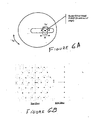
- FIG. 6A is a plan view of an actuator in accordance with the invention which can be fabricated at relatively low expense and is capable of making rapid and automated adjustments of screw mechanisms for altering the shape of an optical element.
- this mechanism is a robotic screw driver with four degrees of freedom.
- the body of the robotic screw driver is preferably in the form of a disk which can be rotated about its center as indicated by arrow Tz.
- a slot is formed in the disk for radial motion R of the screw driver which is moved in the direction Z (into or out of the page) to engage the screw mechanism and then rotated in the direction Tz' to make the adjustment of the screw mechanism.
- the motions R and Tz are sufficient to locate the actuator/screw driver head at any location covered by the disk (e.g. as shown in Figure 6B) and adjustments of any and all such screw mechanisms may be made rapidly in sequence, and a high density array of set-screw mechanisms may be accommodated.
- the dots in the top and side views schematically depict exemplary locations of set screw type adjustment mechanisms (the details of which are unimportant to the practice of the invention).
- the array of such mechanisms shown essentially places the individual mechanisms at the apices of equilateral triangles tiling the area of the optical element.
- the extent of the array is arbitrary and the depiction of Figure 6B may be understood as only a representative portion of the entire array. It can thus be seen that the rotational and radial motions of the robotic screwdriver of Figure 6A is sufficient to align the screw driver head with any location depicted in Figure 6B and coarse incremental motion and/or increase of size of the robotic screwdriver can accommodate an array of arbitrary extent.
- highly stable optical compensation is generally provided if the temperature of the environment is kept relatively stable, especially if weak springs are employed, as discussed above.
- other temperature compensating arrangements can be employed as well.
- the same principles are not limited to set-screw type mechanisms but can be employed to move a single actuator or a small number of actuators of any type to cover a relatively large number of adjustment points.
- a high degree of stability can be obtained in a manner consistent with high spatial resolution of correction by providing for effective maintenance of any adjustment made, supplemented by reduced effects of drift, noise, vibration and heat by avoiding a need for continuous operation of actuators and/or use of very few actuators only as needed.
- a shaft of a linear actuator or shaft connected thereto is attached to the back of a deformable mirror 110 through weak springs 155. Since the weak springs 155 are attached to both the deformable mirror 110 and the actuator shaft 150, a force can be applied in either of two opposite directions (e.g. pushing or pulling on the mirror 110).
- the actuators 140 are illustrated as supported rigidly on a base plate 120 but, as will be discussed below, other arrangements are possible and may be preferable.
- the actuator shafts 150 are individually guided in their motion by a plate 130 which is preferably rigid and of sufficient strength, comparable to that of actuator baseplate 120, to carry the forces of numerous actuator shafts and the forces they collectively impose on the mirror 110.
- a plate 130 which is preferably rigid and of sufficient strength, comparable to that of actuator baseplate 120, to carry the forces of numerous actuator shafts and the forces they collectively impose on the mirror 110.
- rigidity of the base plate 120 and plate 130 is not critical to the practice of the invention if weak springs 155 are employed since the applied force determines the figure of the mirror and will not change significantly over small deflections of the base plate 120 or plate 130.
- Plate 130 is preferably configured as a clamp plate. That is, actuator shaft clamps may be affixed thereto or integrally formed therein (e.g. by machining openings in the clamp plate 130) as will be discussed below.
- the deformable mirror system in accordance with the invention operates by using controller 105 to control actuators 140 to apply forces to the back of deformable mirror 110.
- the actuators may be of any type such as solenoids, fluidic systems, set screws, as alluded to above, and the like.
- the force is changed by compression or elongation of spring 155 through movement of the actuator shaft by the actuator until the desired deformation and force causing it is achieved.
- the deformations of interest to alter the figure of the mirror to correct or compensate other aberrations of the optical system are so small (e.g. on the order of the wavelength of the radiation employed which is very short in the EUV range) that the deformable mirror system may be considered as a linear system. That is, the deformation of the mirror is the linear sum of the deformations of each of the actuators applied individually through whatever mechanism or mechanical linkage is employed.
- clamping mechanisms are actuated using clamp actuators 165 to maintain the position of the actuator shaft(s) at that position.
- the clamps thus assume the load of the actuators and the actuators can be de-energized.
- the clamps can also share the load of set-screw type arrangements while preventing rotational movement due to vibration or the like.
- the clamps can also be arranged very close to the back of the mirror so that only a short portion of the actuator shaft and the spring remains between the clamp and the mirror in order to enhance stability, particularly as to temperature. That is, the positioning of the clamp close to the mirror reduces the length of actuator shaft which is subject to change of dimension due to change in temperature.
- proximity is the length of the weak spring 155 and the need to provide a sufficient range of shaft motion to derive the desired range of force corresponding to the desired range of mirror movement in consideration of the particular spring constant of the weak spring 155.
- change of spring constant and dimensions with temperature, the coefficient of thermal expansion of the actuator shaft and the anticipated range of thermal excursions may also be considered in the design for a particular application but are not critical to the successful practice of the invention.
- both types of actuators become equivalent, and both require the weak spring to isolate the mirror displacement from changes in the clamp plate shape or position or changes in the shaft or spring properties caused by temperature change or possibly small amounts of slip by the clamps.
- the clamps such that the actuators can be de-energized, the actuators are effectively removed from the system as a source of heat or drift.
- the clamps and their actuators can be configured in such a way that the clamp actuators are used only when an adjustment is made and no heat is generated from the clamp actuators 165 when the actuator shafts are clamped.
- de-energization of the actuators 140 and the clamp actuators after proper adjustment is reached also removes drift, noise and vibration as sources of instability in the deformable mirror system.
- actuators 140 are de-energized after adjustment and the system is substantially linear, a reduced number of actuators may be used and the adjustments made serially while allowing actuator shafts 150 to be spaced more closely (e.g. at higher pitch) than the size of actuators 140 might otherwise allow.
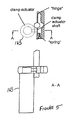
- the clamp is preferably formed with an aperture 210 for receiving the actuator shaft 150 and which is shaped to cause slight but sufficient binding wich the actuator shaft 150 in the clamped position.
- This effect can be easily achieved by the preferred expedient of providing for opening of the clamp at diametrically opposite sides of the aperture 210 such that the movable clamp jaw 220 can be deformed slightly by a cam-like action as it presses against the actuator shaft 150, preferably under the influence of a force such as may be provided by a spring which will maintain the clamp in a clamped position when the clamp actuator 165 is de-energized.
- Clamp jaw 230 can be either fixed or movable. It is considered preferable that both clamp jaws be moved away from the actuator shaft as positioned by the clamp plate 130 by the clamp actuator 165, when energized. Alternatively, if one of the clamps is fixed, it could be located at a slight distance from the actuator shaft, so that when the mobile clamp jaw is activated it pushes the shaft against the fixed jaw.
- the clamp jaws are preferably shaped slightly differently from the shaft, so that when they close on the actuator, the applied force is over a restricted area of contact. This ensures a more secure clamping force and avoids the chance of the two components binding together and abrading their surfaces.
- the shaft of the actuator is of circular cross section
- the clamp shape may be arc shaped, with a radius of curvature greater than the shaft radius.
- Figure 2 is representative of an embodiment of the invention using discrete clamps and clamp actuators mounted on a clamp plate 130.
- the clamp structure can be integrally formed in the clamp plate 130, as depicted in Figures 3A and 3B, as will now be discussed.
- Figure 3A shows an array of clamps 300 and clamp actuators 165 where the clamps and the actuator springs 310 are integrally formed in the clamp plate 130.
- the use of the material of the clamp plate to form clamp springs is not inconsistent with the requirement for rigidity and stiffness of the clamp plate 130 since the clamp plate can be as thick as necessary to achieve sufficient stiffness and rigidity while minor deflection of the clamp plate is not critical if weak springs 155 are employed, as discussed above.
- the material of the clamp plate 130 is not critical to the practice of the invention.
- the clamp plate with integral clamps and springs may be formed by any desired technique such as casting, molding or the like but machining is preferred for high precision and yield.
- the machining process is not critical, and milling, electric discharge machining, laser ablation and the like or a combination thereof can be used.
- Figure 3B shows a single clamp 300 and clamp actuator 165 in plan view and cross-section.
- the area 305 identified by cross-hatching is removed from the clamp plate.
- Area 305 comprises essentially two long slots 301, 302, with two additional short slots 303, 304, which are interdigitated to form a spring 310.
- Slots 301, 302 are separated but closely approach each other at one end in order to form a hinge 320.
- the material between the slots forms a clamp bar 330, generally corresponding co moveable clamp jaw 220 of Figure 2.
- the configuration of the clamp bar should largely avoid the formation of a hinge structure adjacent the actuator shaft aperture by providing a relatively constant thickness of clamp bar 330, as shown, but some degree of flexibility at that point may enhance the binding action of the clamp.
- Other configurations of the cut-out are also possible but the pattern illustrated in Figure 3B is considered to be preferred.
- the actuator shaft 340 of clamp actuator 165 is preferably held in a recess formed in clamp plate 130 and an aperture to allow appropriate and convenient insertion into the recess and a mechanical coupling to the actuator is provided, preferably as shown.
- details of the shaft location and installation are not critical to the practice of the invention, as long as the clamp actuator shaft can bear against and move clamp bar 330 to increase separation from the remainder of the clamp plate and allow actuator shaft 140 to freely move in the axial direction. This motion will be opposed by deformation of the two cantilevers formed by short slots 303 and 304 forming a return spring 310 which will cause clamping to be resumed when clamp actuator 165 is de-energized or turned off.
- the integrally formed clamp 300 functions in the same manner as the discrete clamp embodiment of Figure 2 but has the added advantages of allowing a more simple actuator which may be of any type (e.g. electromagnetic, fluidic, mechanical and the like) and providing an integral return spring 310 that need not be included in actuator 165 while providing a more robust clamp.
- a more simple actuator which may be of any type (e.g. electromagnetic, fluidic, mechanical and the like) and providing an integral return spring 310 that need not be included in actuator 165 while providing a more robust clamp.
- the integrally formed clamp of Figure 3A and 3B occupies somewhat more space on the clamp plate 130 than might be required by a discrete clamp.
- the size of the clamp actuators may further limit actuator shaft spacing pitch or density or even be controlling of the spatial frequency of control of the mirror shape which can be provided.
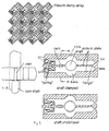
- accommodation of actuator shafts at higher spatial frequency can be provided by clamps in complementary and inter-digitated arrays on two or more levels using two or more clamp plates 130a, 130b as shown in Figure 4. This configuration also provides for the loads supporting forces on the mirror to be divided and the thickness of each of the clamp plates can be correspondingly reduced.
- Clamp actuators may be placed on either or both surfaces of the of the clamp plate 130 or plates 130a, 130b.
- actuator size may be accommodated consistent with high actuator shaft location pitch by orienting the actuators parallel to the actuator shafts 140 as shown in Figure 5.
- Rotary actuators may also be accommodated in this fashion.
- a cam can be used in place of clamp actuator shaft 340. In this case, space can be saved by placement of the actuator over a portion of the clamp and, further, allows a single clamp actuator to be moved across the clamp plate 130 to operate clamps serially by inserting a cam of, for example, elliptical cross-section into slot 302.
- the clamp actuator 165 that drives cam 810 could be mounted on the same carriage as an actuator 140 since the clamp plate 130 and actuator base plate 120 are in different planes and suitably moved among the array of actuator shafts 140 to carry out a sequence of adjustments.
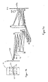
- FIG. 9 A further variation of the preferred embodiment of the invention is illustrated in Figure 9.
- clamp jaw 220 was movable and clamp jaw 230 was optionally but preferably moveable.
- clamp bar 330 generally corresponding to clamp jaw 220 is moveable while the jaw corresponding to jaw 230 is formed in the base plate is stationary and would involve asymmetrical or eccentric operation of a cam in order to avoid directional (e.g. non-rotational) forces parallel to the clamp plate being placed on an actuator.
- the asymmetrical clamp action may also cause undesirable lateral shifting motion of the actuator shaft 140 that may be coupled to the mirror.
- a deformable mirror system in which stability of adjustments and corrections made is improved while effects such as actuator drift, noise, vibration and heating are substantially avoided.
- the invention also allows a single actuator or a reduced number of actuators to be shared among a plurality of actuator shafts and/or clamps, respectively, and supports provision of actuator shafts at increased density or pitch.
- a single actuator can be shared among a plurality of clamps, as well.
- Discrete or integrally formed clamps may be provided as may be desired to accommodate application of the invention at any scale and complexity and provides a practical technique for improving the performance of EUV lithographic tools in particular.
Applications Claiming Priority (4)
| Application Number | Priority Date | Filing Date | Title |
|---|---|---|---|
| US39015802P | 2002-06-21 | 2002-06-21 | |
| US390158P | 2002-06-21 | ||
| US373687 | 2003-02-27 | ||
| US10/373,687 US6989922B2 (en) | 2002-06-21 | 2003-02-27 | Deformable mirror actuation system |
Publications (1)
| Publication Number | Publication Date |
|---|---|
| EP1376191A1 true EP1376191A1 (fr) | 2004-01-02 |
Family
ID=29718524
Family Applications (1)
| Application Number | Title | Priority Date | Filing Date |
|---|---|---|---|
| EP03013979A Withdrawn EP1376191A1 (fr) | 2002-06-21 | 2003-06-20 | Système d' actionnement d' un miroir deformable |
Country Status (3)
| Country | Link |
|---|---|
| US (1) | US6989922B2 (fr) |
| EP (1) | EP1376191A1 (fr) |
| JP (1) | JP2004047994A (fr) |
Cited By (7)
| Publication number | Priority date | Publication date | Assignee | Title |
|---|---|---|---|---|
| EP1378782A2 (fr) * | 2002-07-03 | 2004-01-07 | Nikon Corporation | Miroir déformable équipé d'actionneurs passifs et actifs |
| US7125128B2 (en) | 2004-01-26 | 2006-10-24 | Nikon Corporation | Adaptive-optics actuator arrays and methods for using such arrays |
| WO2007031271A1 (fr) * | 2005-09-13 | 2007-03-22 | Carl Zeiss Smt Ag | Système optique de projection pour microlithographie, procédé de fabrication d’un dispositif et procédé de conception d’une surface optique |
| US8094380B2 (en) | 2006-03-27 | 2012-01-10 | Carl Zeiss Smt Gmbh | Projection objective and projection exposure apparatus with negative back focus of the entry pupil |
| CN103268013A (zh) * | 2013-06-06 | 2013-08-28 | 清华大学 | 变形镜 |
| WO2013184261A3 (fr) * | 2012-06-04 | 2014-01-30 | The Boeing Company | Miroir correcteur modal ayant un fonctionnement compliant pour des aberrations optiques |
| CN101416117B (zh) * | 2006-04-07 | 2014-11-05 | 卡尔蔡司Smt有限责任公司 | 微光刻投影光学系统、工具及其制造方法 |
Families Citing this family (29)
| Publication number | Priority date | Publication date | Assignee | Title |
|---|---|---|---|---|
| JP2002277736A (ja) * | 2001-03-21 | 2002-09-25 | Olympus Optical Co Ltd | 撮像装置 |
| JP4565908B2 (ja) * | 2004-06-25 | 2010-10-20 | 株式会社大日本科研 | 非球面コリメートミラーの調整方法 |
| JP4843272B2 (ja) * | 2004-07-31 | 2011-12-21 | カール・ツァイス・エスエムティー・ゲーエムベーハー | マイクロリソグラフィ投影露光装置の光学システム |
| US20060077579A1 (en) * | 2004-10-12 | 2006-04-13 | Margeson Christopher S | Force actuator with clamp |
| FR2877104B1 (fr) * | 2004-10-27 | 2006-12-29 | Sagem | Dispositif d'imagerie ou d'insolation, notamment pour la realisation d'un micro-circuit electronique |
| US7422988B2 (en) * | 2004-11-12 | 2008-09-09 | Applied Materials, Inc. | Rapid detection of imminent failure in laser thermal processing of a substrate |
| JP4817702B2 (ja) * | 2005-04-14 | 2011-11-16 | キヤノン株式会社 | 光学装置及びそれを備えた露光装置 |
| JP2007058920A (ja) * | 2005-08-22 | 2007-03-08 | Funai Electric Co Ltd | 形状可変ミラー及びそれを備えた光ピックアップ装置並びに形状可変ミラーの製造方法 |
| US7652759B1 (en) | 2006-02-23 | 2010-01-26 | Rockwell Automation Technologies, Inc. | Industrial device with adaptive optics |
| US7633630B2 (en) * | 2006-08-09 | 2009-12-15 | Northrop Grumman Corporation | Image amplifying, servo-loop controlled, point diffraction interometer |
| EP2105239B1 (fr) * | 2006-11-30 | 2016-01-13 | Sumitomo Electric Industries, Ltd. | Systeme optique de condensation de lumiere, procede et appareil de traitement laser, et procede de fabrication de materiau fragile |
| US8416386B2 (en) * | 2007-03-13 | 2013-04-09 | Nikon Corporation | Conforming seats for clamps used in mounting an optical element, and optical systems comprising same |
| US7967456B2 (en) * | 2007-11-02 | 2011-06-28 | The United States Of America As Represented By The Secretary Of The Army | Scalable size deformable pocket mirror with on-pocket bimorph actuator |
| US8002420B2 (en) * | 2008-07-23 | 2011-08-23 | Nikon Corporation | Hydrostatic liquid-metal deformable optical elements |
| US9041900B2 (en) | 2008-10-30 | 2015-05-26 | Nikon Corporation | High heat load optics with a liquid metal interface for use in an extreme ultraviolet lithography system |
| US8739383B2 (en) * | 2009-04-20 | 2014-06-03 | Nikon Corporation | Method and apparatus for aligning mirror blocks of a multi-element mirror assembly |
| JP5556155B2 (ja) * | 2009-12-04 | 2014-07-23 | 株式会社ニコン | 光学部材変形装置、光学系、露光装置、デバイスの製造方法 |
| JP2011119551A (ja) * | 2009-12-04 | 2011-06-16 | Nikon Corp | 光学部材変形装置、光学系、露光装置、デバイスの製造方法 |
| WO2012000528A1 (fr) * | 2010-07-01 | 2012-01-05 | Carl Zeiss Smt Gmbh | Système optique et miroir à facettes multiples |
| FR2973168B1 (fr) * | 2011-03-24 | 2013-05-17 | Thales Sa | Systeme d'actionnement pour reflecteur d'antenne a surface reflechissante deformable |
| WO2013022892A1 (fr) * | 2011-08-11 | 2013-02-14 | Nikon Corporation | Commande de température intermittente d'éléments optiques mobiles |
| DE102012212757A1 (de) | 2012-07-20 | 2014-01-23 | Carl Zeiss Smt Gmbh | Verfahren zum betreiben einer mikrolithographischen projektionsbelichtungsanlage |
| KR102390697B1 (ko) | 2013-01-28 | 2022-04-26 | 에이에스엠엘 네델란즈 비.브이. | 리소그래피 장치를 위한 방사선 소스, 거울 및 투영 시스템 |
| JP2014225639A (ja) * | 2013-04-16 | 2014-12-04 | キヤノン株式会社 | ミラーユニット及び露光装置 |
| US9529282B2 (en) | 2013-04-25 | 2016-12-27 | Nikon Corporation | Position-measurement systems |
| US9577344B2 (en) * | 2013-11-27 | 2017-02-21 | The United States of Americ as represented by the Secretary of the Air Force | Actuated pin antenna reflector |
| DE102014209151A1 (de) * | 2014-05-14 | 2015-07-02 | Carl Zeiss Smt Gmbh | Optisches Modul |
| US10883924B2 (en) | 2014-09-08 | 2021-01-05 | The Research Foundation Of State University Of New York | Metallic gratings and measurement methods thereof |
| US11143965B2 (en) * | 2019-04-30 | 2021-10-12 | Taiwan Semiconductor Manufacturing Company, Ltd. | Optical lithography system for patterning semiconductor devices and method of using the same |
Citations (5)
| Publication number | Priority date | Publication date | Assignee | Title |
|---|---|---|---|---|
| US4940318A (en) * | 1988-11-03 | 1990-07-10 | Itek Corporation | Gradient membrane deformable mirror having replaceable actuators |
| US5210653A (en) * | 1992-06-08 | 1993-05-11 | Schell John D | External actuator for a deformable mirror |
| US6198180B1 (en) * | 1999-06-30 | 2001-03-06 | Sandia Corporation | Micromechanisms with floating pivot |
| US6384952B1 (en) * | 1997-03-27 | 2002-05-07 | Mems Optical Inc. | Vertical comb drive actuated deformable mirror device and method |
| WO2003010568A1 (fr) * | 2001-07-24 | 2003-02-06 | Santur Corporation | Ensemble de lasers regules accordables |
Family Cites Families (10)
| Publication number | Priority date | Publication date | Assignee | Title |
|---|---|---|---|---|
| US4655563A (en) | 1985-11-25 | 1987-04-07 | Itek Corporation | Variable thickness deformable mirror |
| US4967063A (en) | 1988-06-16 | 1990-10-30 | The Aerospace Corporation | Charge controlled adaptive-optics system |
| US4950878A (en) | 1989-04-12 | 1990-08-21 | Kaman Aerospace Corporation | Wavefront control system using optical coarse/fine gradient sensor |
| JP3259373B2 (ja) | 1992-11-27 | 2002-02-25 | 株式会社日立製作所 | 露光方法及び露光装置 |
| US5745309A (en) | 1994-06-13 | 1998-04-28 | The United States Of America As Represented By The United States Department Of Energy | Method for removing tilt control in adaptive optics systems |
| US5687566A (en) * | 1995-05-15 | 1997-11-18 | Petty; Jon A. | Arrangement and method for removal of air from a hydraulic system |
| US5684566A (en) | 1995-05-24 | 1997-11-04 | Svg Lithography Systems, Inc. | Illumination system and method employing a deformable mirror and diffractive optical elements |
| US5815310A (en) | 1995-12-12 | 1998-09-29 | Svg Lithography Systems, Inc. | High numerical aperture ring field optical reduction system |
| US5912731A (en) | 1997-12-04 | 1999-06-15 | Trw Inc. | Hartmann-type optical wavefront sensor |
| US6464364B2 (en) * | 2000-01-27 | 2002-10-15 | Aoptix Technologies, Inc. | Deformable curvature mirror |
-
2003
- 2003-02-27 US US10/373,687 patent/US6989922B2/en not_active Expired - Fee Related
- 2003-06-18 JP JP2003173242A patent/JP2004047994A/ja active Pending
- 2003-06-20 EP EP03013979A patent/EP1376191A1/fr not_active Withdrawn
Patent Citations (5)
| Publication number | Priority date | Publication date | Assignee | Title |
|---|---|---|---|---|
| US4940318A (en) * | 1988-11-03 | 1990-07-10 | Itek Corporation | Gradient membrane deformable mirror having replaceable actuators |
| US5210653A (en) * | 1992-06-08 | 1993-05-11 | Schell John D | External actuator for a deformable mirror |
| US6384952B1 (en) * | 1997-03-27 | 2002-05-07 | Mems Optical Inc. | Vertical comb drive actuated deformable mirror device and method |
| US6198180B1 (en) * | 1999-06-30 | 2001-03-06 | Sandia Corporation | Micromechanisms with floating pivot |
| WO2003010568A1 (fr) * | 2001-07-24 | 2003-02-06 | Santur Corporation | Ensemble de lasers regules accordables |
Cited By (17)
| Publication number | Priority date | Publication date | Assignee | Title |
|---|---|---|---|---|
| EP1378782A3 (fr) * | 2002-07-03 | 2005-01-26 | Nikon Corporation | Miroir déformable équipé d'actionneurs passifs et actifs |
| EP1378782A2 (fr) * | 2002-07-03 | 2004-01-07 | Nikon Corporation | Miroir déformable équipé d'actionneurs passifs et actifs |
| US7572019B2 (en) | 2004-01-26 | 2009-08-11 | Nikon Corporation | Adaptive-optics actuator arrays and methods for using such arrays |
| US7125128B2 (en) | 2004-01-26 | 2006-10-24 | Nikon Corporation | Adaptive-optics actuator arrays and methods for using such arrays |
| US8169694B2 (en) | 2005-09-13 | 2012-05-01 | Carl Zeiss Smt Gmbh | Catoptric objectives and systems using catoptric objectives |
| US7414781B2 (en) | 2005-09-13 | 2008-08-19 | Carl Zeiss Smt Ag | Catoptric objectives and systems using catoptric objectives |
| US7719772B2 (en) | 2005-09-13 | 2010-05-18 | Carl Zeiss Smt Ag | Catoptric objectives and systems using catoptric objectives |
| WO2007031271A1 (fr) * | 2005-09-13 | 2007-03-22 | Carl Zeiss Smt Ag | Système optique de projection pour microlithographie, procédé de fabrication d’un dispositif et procédé de conception d’une surface optique |
| US9465300B2 (en) | 2005-09-13 | 2016-10-11 | Carl Zeiss Smt Gmbh | Catoptric objectives and systems using catoptric objectives |
| US8094380B2 (en) | 2006-03-27 | 2012-01-10 | Carl Zeiss Smt Gmbh | Projection objective and projection exposure apparatus with negative back focus of the entry pupil |
| US8810927B2 (en) | 2006-03-27 | 2014-08-19 | Carl Zeiss Smt Gmbh | Projection objective and projection exposure apparatus with negative back focus of the entry pupil |
| CN101416117B (zh) * | 2006-04-07 | 2014-11-05 | 卡尔蔡司Smt有限责任公司 | 微光刻投影光学系统、工具及其制造方法 |
| US8970819B2 (en) | 2006-04-07 | 2015-03-03 | Carl Zeiss Smt Gmbh | Microlithography projection optical system, tool and method of production |
| US9482961B2 (en) | 2006-04-07 | 2016-11-01 | Carl Zeiss Smt Gmbh | Microlithography projection optical system, tool and method of production |
| WO2013184261A3 (fr) * | 2012-06-04 | 2014-01-30 | The Boeing Company | Miroir correcteur modal ayant un fonctionnement compliant pour des aberrations optiques |
| US9500855B2 (en) | 2012-06-04 | 2016-11-22 | The Boeing Company | Modal corrector mirror with compliant actuation for optical aberrations |
| CN103268013A (zh) * | 2013-06-06 | 2013-08-28 | 清华大学 | 变形镜 |
Also Published As
| Publication number | Publication date |
|---|---|
| JP2004047994A (ja) | 2004-02-12 |
| US6989922B2 (en) | 2006-01-24 |
| US20030234970A1 (en) | 2003-12-25 |
Similar Documents
| Publication | Publication Date | Title |
|---|---|---|
| US6989922B2 (en) | Deformable mirror actuation system | |
| US6840638B2 (en) | Deformable mirror with passive and active actuators | |
| KR100791161B1 (ko) | 광학장치 및 그것을 구비한 노광장치 | |
| US6967756B2 (en) | Lithographic apparatus device manufacturing method and device manufactured thereby | |
| JP3567152B2 (ja) | リソグラフィック装置、デバイス製造方法、およびその方法により製造したデバイス | |
| JP3931039B2 (ja) | リソグラフィ投影装置およびこれを使ったデバイスの製造方法 | |
| JP4314237B2 (ja) | リソグラフィ装置、デバイス製造方法、及びリソグラフィ装置用の投影要素 | |
| US10061206B2 (en) | Projection lens with wave front manipulator and related method and apparatus | |
| US20060072219A1 (en) | Mirror holding mechanism in exposure apparatus, and device manufacturing method | |
| KR100573665B1 (ko) | 리소그래피장치 및 디바이스 제조방법 | |
| US7352475B2 (en) | Measuring method and apparatus using shearing interferometry, exposure method and apparatus using the same, and device manufacturing method | |
| JP4883775B2 (ja) | 光学装置、露光装置及びデバイス製造方法 | |
| US6977728B2 (en) | Projection exposure apparatus and aberration measurement method | |
| EP1107068B1 (fr) | Appareil de projection lithographique avec système de positionnement d'un réflecteur | |
| JP4495115B2 (ja) | リソグラフィ装置及びリソグラフィ方法 | |
| KR101470650B1 (ko) | 광학 부재 보지 장치, 광학 부재의 위치 조정 방법 및 노광장치 | |
| JP3708075B2 (ja) | リソグラフィ装置およびデバイス製造方法 | |
| EP1174770A2 (fr) | Appareil lithographique | |
| EP1231515A1 (fr) | Appareil lithographique et méthode de fabrication d'un dispositif | |
| Ballard et al. | System and process learning in a full-field high-power EUVL alpha tool |
Legal Events
| Date | Code | Title | Description |
|---|---|---|---|
| PUAI | Public reference made under article 153(3) epc to a published international application that has entered the european phase |
Free format text: ORIGINAL CODE: 0009012 |
|
| AK | Designated contracting states |
Kind code of ref document: A1 Designated state(s): AT BE BG CH CY CZ DE DK EE ES FI FR GB GR HU IE IT LI LU MC NL PT RO SE SI SK TR |
|
| AX | Request for extension of the european patent |
Extension state: AL LT LV MK |
|
| 17P | Request for examination filed |
Effective date: 20040504 |
|
| AKX | Designation fees paid |
Designated state(s): DE NL |
|
| 17Q | First examination report despatched |
Effective date: 20050214 |
|
| STAA | Information on the status of an ep patent application or granted ep patent |
Free format text: STATUS: THE APPLICATION IS DEEMED TO BE WITHDRAWN |
|
| 18D | Application deemed to be withdrawn |
Effective date: 20050625 |