EP1374381B1 - Vorrichtung zur transformation einer primärspannung in eine sekundärspannung mit mindestens einem schaltnetzteil - Google Patents
Vorrichtung zur transformation einer primärspannung in eine sekundärspannung mit mindestens einem schaltnetzteil Download PDFInfo
- Publication number
- EP1374381B1 EP1374381B1 EP02724271A EP02724271A EP1374381B1 EP 1374381 B1 EP1374381 B1 EP 1374381B1 EP 02724271 A EP02724271 A EP 02724271A EP 02724271 A EP02724271 A EP 02724271A EP 1374381 B1 EP1374381 B1 EP 1374381B1
- Authority
- EP
- European Patent Office
- Prior art keywords
- circuit
- primary
- transformer
- output
- oscillating circuit
- Prior art date
- Legal status (The legal status is an assumption and is not a legal conclusion. Google has not performed a legal analysis and makes no representation as to the accuracy of the status listed.)
- Expired - Lifetime
Links
Images


Classifications
-
- H—ELECTRICITY
- H02—GENERATION; CONVERSION OR DISTRIBUTION OF ELECTRIC POWER
- H02M—APPARATUS FOR CONVERSION BETWEEN AC AND AC, BETWEEN AC AND DC, OR BETWEEN DC AND DC, AND FOR USE WITH MAINS OR SIMILAR POWER SUPPLY SYSTEMS; CONVERSION OF DC OR AC INPUT POWER INTO SURGE OUTPUT POWER; CONTROL OR REGULATION THEREOF
- H02M3/00—Conversion of DC power input into DC power output
- H02M3/22—Conversion of DC power input into DC power output with intermediate conversion into AC
- H02M3/24—Conversion of DC power input into DC power output with intermediate conversion into AC by static converters
- H02M3/28—Conversion of DC power input into DC power output with intermediate conversion into AC by static converters using discharge tubes with control electrode or semiconductor devices with control electrode to produce the intermediate AC
- H02M3/325—Conversion of DC power input into DC power output with intermediate conversion into AC by static converters using discharge tubes with control electrode or semiconductor devices with control electrode to produce the intermediate AC using devices of a triode or a transistor type requiring continuous application of a control signal
- H02M3/335—Conversion of DC power input into DC power output with intermediate conversion into AC by static converters using discharge tubes with control electrode or semiconductor devices with control electrode to produce the intermediate AC using devices of a triode or a transistor type requiring continuous application of a control signal using semiconductor devices only
- H02M3/337—Conversion of DC power input into DC power output with intermediate conversion into AC by static converters using discharge tubes with control electrode or semiconductor devices with control electrode to produce the intermediate AC using devices of a triode or a transistor type requiring continuous application of a control signal using semiconductor devices only in push-pull configuration
- H02M3/3376—Conversion of DC power input into DC power output with intermediate conversion into AC by static converters using discharge tubes with control electrode or semiconductor devices with control electrode to produce the intermediate AC using devices of a triode or a transistor type requiring continuous application of a control signal using semiconductor devices only in push-pull configuration with automatic control of output voltage or current
-
- H—ELECTRICITY
- H02—GENERATION; CONVERSION OR DISTRIBUTION OF ELECTRIC POWER
- H02M—APPARATUS FOR CONVERSION BETWEEN AC AND AC, BETWEEN AC AND DC, OR BETWEEN DC AND DC, AND FOR USE WITH MAINS OR SIMILAR POWER SUPPLY SYSTEMS; CONVERSION OF DC OR AC INPUT POWER INTO SURGE OUTPUT POWER; CONTROL OR REGULATION THEREOF
- H02M3/00—Conversion of DC power input into DC power output
- H02M3/22—Conversion of DC power input into DC power output with intermediate conversion into AC
- H02M3/24—Conversion of DC power input into DC power output with intermediate conversion into AC by static converters
- H02M3/28—Conversion of DC power input into DC power output with intermediate conversion into AC by static converters using discharge tubes with control electrode or semiconductor devices with control electrode to produce the intermediate AC
- H02M3/325—Conversion of DC power input into DC power output with intermediate conversion into AC by static converters using discharge tubes with control electrode or semiconductor devices with control electrode to produce the intermediate AC using devices of a triode or a transistor type requiring continuous application of a control signal
- H02M3/335—Conversion of DC power input into DC power output with intermediate conversion into AC by static converters using discharge tubes with control electrode or semiconductor devices with control electrode to produce the intermediate AC using devices of a triode or a transistor type requiring continuous application of a control signal using semiconductor devices only
- H02M3/338—Conversion of DC power input into DC power output with intermediate conversion into AC by static converters using discharge tubes with control electrode or semiconductor devices with control electrode to produce the intermediate AC using devices of a triode or a transistor type requiring continuous application of a control signal using semiconductor devices only in a self-oscillating arrangement
- H02M3/3385—Conversion of DC power input into DC power output with intermediate conversion into AC by static converters using discharge tubes with control electrode or semiconductor devices with control electrode to produce the intermediate AC using devices of a triode or a transistor type requiring continuous application of a control signal using semiconductor devices only in a self-oscillating arrangement with automatic control of output voltage or current
-
- Y—GENERAL TAGGING OF NEW TECHNOLOGICAL DEVELOPMENTS; GENERAL TAGGING OF CROSS-SECTIONAL TECHNOLOGIES SPANNING OVER SEVERAL SECTIONS OF THE IPC; TECHNICAL SUBJECTS COVERED BY FORMER USPC CROSS-REFERENCE ART COLLECTIONS [XRACs] AND DIGESTS
- Y02—TECHNOLOGIES OR APPLICATIONS FOR MITIGATION OR ADAPTATION AGAINST CLIMATE CHANGE
- Y02B—CLIMATE CHANGE MITIGATION TECHNOLOGIES RELATED TO BUILDINGS, e.g. HOUSING, HOUSE APPLIANCES OR RELATED END-USER APPLICATIONS
- Y02B70/00—Technologies for an efficient end-user side electric power management and consumption
- Y02B70/10—Technologies improving the efficiency by using switched-mode power supplies [SMPS], i.e. efficient power electronics conversion e.g. power factor correction or reduction of losses in power supplies or efficient standby modes
Definitions
- the invention relates to a device for transforming a primary voltage into a secondary voltage with at least one switching power supply that is on the resonance converter principle based on phase shifter, such as. B. from US-A-6 178 099 and US-A-5 910 886.
- Switching power supplies are known in principle and are available in a variety of Refinements carried out. Like any electrical consumer cause also switching power supplies electrical losses. Because of the abundance of applications For switching power supplies, efforts are made to reduce the power losses as low as possible to keep. One way of realizing the smallest possible power loss is to miniaturize the switching power supplies.
- the invention is based on the object of a switching power supply for transformation to create a primary voltage into a secondary voltage due to extremely low power loss, effective energy transfer and distinguishes extremely small dimensions.
- the switching power supply according to the invention works on the so-called resonance converter principle.
- the special feature according to the invention is that that both on the primary side and on the secondary side of the actual transformer resonant oscillating circuits are provided.
- This Oscillating circuits are considering their supply and connection lines and especially taking into account those caused by these lines parasitic capacitances and inductors.
- the primary and the secondary winding of the transformer are also part of the primary and the secondary resonant circuit.
- Both resonant circuits have essentially the same resonance frequency on. Ideally, the resonance frequencies are identical. The goodness of the the two resonant circuits are essentially the same. Because the transfer ratio of the transformer logically deviates from the ratio 1: 1, the qualities of both resonant circuits cannot be exactly the same. According to the invention it is provided here that the difference between the grades of both Resonant circuits is as small as possible.
- low-pass filters Located on the input and output sides of the switching power supply according to the invention low-pass filters, whose inductors are magnetically decoupled.
- the exit the low-pass filter on the input side is connected to a driver circuit, which is a full transistor bridge circuit.
- the individual transistors of this driver circuit are via a control device driven.
- This control device has a pulse generator, which Control pulses generated for the individual transistors.
- the phase position of this Control pulses are generated by a phase shifter of the control unit.
- This phase shifter receives from a current and / or voltage sensor an input signal. This sensor senses which current or what voltage is currently given at the output of the switching power supply.
- a rectifier circuit is located on the output side in front of the low-pass filter. During the transistor full bridge driver circuit part of the primary resonant circuit is, the rectifier circuit is part of the secondary resonant circuit. Both resonant circuits are via the magnetic coupling element of the transformer coupled. The capacities and inductors Both resonant circuits include the primary and secondary windings of the transformer, the length and design of the supply lines and Connection lines of the individual elements of the resonant circuits and Elements of the driver circuit or the rectifier circuit designed.
- the housing of the switching power supply according to the invention is at least partially of the magnetic elements of the inductors of the two low-pass filters educated. These parts of the housing are magnetically decoupled. advantageously, the housing is constructed in two parts, with each part magnetically one of the two low-pass filters is coupled and both housing parts are in turn decoupled from one another.
- a metal housing in this case in particular ferromagnetic material
- Electromagnetic compatibility is an advantage.
- Dirac impulses or Gaussian-like, e-functional-like or cosine square function-like pulses are used. All of these pulse forms can be used if the primary resonant circuit is a parallel resonant circuit or in series production.
- the clock frequency is expediently greater than some kHz and in particular greater than 500 kHz, preferably greater than 1 MHz. at these frequencies, as mentioned, can be rectified at the input become. This means that there is no need for voluminous capacitors on the primary side, as usually required for rectification possible.
- the transformer has a primary winding and a secondary winding. These windings can be in thin-film technology or as wire windings be executed.
- the magnetic circuit of the transformer which is preferred is designed as a planar transformer, is in each case a particular closed ferromagnetic material.
- circuit board e.g. B. flip-chip or chip-on-board technology applied and bonded to the conductor tracks.
- a circuit board e.g. B. flip-chip or chip-on-board technology applied and bonded to the conductor tracks.
- the length and shape The traces on the circuit board are according to the desired Resonance frequency and the qualities of the two resonant circuits selected.
- the circuit board can be rigid, flexible or in rigid-flex technology his.
- the current and / or voltage sensor is arranged on the secondary side, its output signal is galvanically decoupled and fed to the phase shifter. This is done for example via an optocoupler.
- Electrical isolation can be dispensed with if the sensor is connected on the primary side. In this case it is part of the primary resonant circuit.
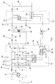
- Fig. 1 the electrical circuit of the switching power supply is shown, which for DC / DC, DC / AC, AC / DC or AC / AC conversion can be used.
- an optional rectifier circuit 12 which is designed as a full diode bridge. With the output of this rectifier 12 is a first low-pass filter 14 with an inductance 16 and a capacitance 18 connected.
- a transistor full-bridge driver circuit is located parallel to the capacitor 18 20, consisting of four transistors 22,24,26,28 with these diodes 23, 25, 27, 29 connected in parallel.
- the control connections 30 of the Transistors 22-28 are connected to a pulse generator 32 by a Phase shifter receives 34 input signals.
- the pulse generator 32 and the Phase shifters 34 together form a control unit 36 for controlling the Driver circuit 20 such that at the output of the switching power supply desired service is available.
- the bridge arm of the driver circuit 20 is with a primary resonant circuit 38 connected, which has an inductance 40 and a capacitance 42 and as Series resonant circuit is formed. Is part of this primary resonant circuit 38 but also the primary winding 44 of a transformer 46, which also has a secondary winding 48 and a magnetic coupling element 50.
- the secondary winding 48 of the transformer 46 is part of a secondary resonant circuit 52, which also has an inductor 54 and a Has capacitance 56 and with which the input of an output-side rectifier circuit 57 is connected.
- This rectifier circuit 57 is also designed as a full diode bridge and has one in its output second Current or voltage sensor 58.
- the sensor 58 outputs an optocoupler 60 a representative of the sensed quantity (current and / or voltage) Output signal to the phase shifter 34 of the control unit 36.
- An output-side low-pass filter 62 is located behind the sensor 58 an inductor 64 and a capacitance 66.
- the switching power supply works with a resonance converter.
- the peculiarity of this resonance converter exists in that both resonant circuits 38, 52 are the same or essentially the same have the same resonance frequency.
- the inductance and capacitance of the two resonant circuits 38, 52 and the windings 44 and 48 of the transformer 46 are arranged on a printed circuit board 68 (see FIGS. 2 to 5).
- the Conductor tracks on this circuit board 68 are of their design and length designed so that the parasitic effects they cause (Inductance and capacitance) adjust so that both resonant circuits 38.52 have the same resonance frequency.
- the semiconductor components of the transistor full-bridge driver circuit also go 20 and the rectifier circuit 57 with.
- the 70.72 are, as can also be seen in FIG. 1.
- the first includes 70 the control unit 36 and the driver circuit 20, while the second die 72 comprises the rectifier circuit 57 and the sensor 58.
- These two dies 70,72 are realized in BGA technology and directly on the Printed circuit board 68 soldered or glued (flip-chip technology), specifically for one on top 74 and the other on bottom 76 of the circuit board 68 (see FIGS. 2 and 3).
- Alternative techniques are bonding, e.g. B. TAB.
- the microintegration enables the resonance frequencies of both Oscillating circuits - including the conductor track designs and components interpret the same value through simulation and design.
- the transformer 46 ratio is a complete one It is not possible to match the qualities of both resonant circuits 38.52. Ideally these two grades should also be identical, which is indicated by a corresponding one Choice of the dimensioning and design of the individual components can realize.
- the aim of the circuit design is therefore to make the grades so to get as close as possible to each other. This then results overall an almost optimal and largely lossless energy transfer from Primary resonant circuit 38 to the secondary resonant circuit 52.
- the phase shifter 34 still has a further output 78 and a further input 80.
- About these Inputs and outputs 78, 80 can be the control unit 36 of the one shown in FIG. 1 Connect the switching power supply to another switching power supply. This creates a modular design in terms of circuitry, which makes it possible to have several switched-mode power supplies combine with each other to create certain output voltages to realize or streams.
- Dirac pulses in particular 2nd order or Dirac double pulses or pulses, whose shape can be described in accordance with one of the equations given below, are preferably used to control the transistors 22, 24, 26 and 28.
- f (x) ae -bx 2
- f (x) a cos 2 (Bx)
- f (x) a sin x / x
- These pulses are generated at a frequency greater than 500kHz and in particular generated with a frequency in the MHz range.
- a high Switching frequency is a rectification of the input voltage, as in the 1 in the form of the rectifier circuit 12 is provided, not mandatory.
- the rectifier circuit 12 is not necessarily Part of the switching power supply described here.
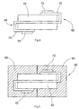
- FIGS. Played 2-5 The structure of the switching power supply in microintegration technology is shown in FIGS. Played 2-5. It can also be seen there that the transformer 46 as so-called planar transformer is constructed in thin-film technology. in this connection are the primary and secondary windings 44.48 as z. B. round, oval, elliptical, rectangular, spiral-shaped conductor tracks of the printed circuit board 68 formed, with the conductor tracks of the primary winding 44 on the top 74 and the conductor tracks of the secondary winding 48 on the underside 76 of the Printed circuit board 68 are formed. The spiral tracks of primary and Secondary winding 44,48 are through the magnetic coupling element 50 enclosed, which extends above and below the circuit board 68.
- the circuit board 68 is preferably designed to be flexible throughout and on their ends 82, 84 projecting laterally from the coupling element 50 in opposite directions around the magnetic coupling element 50 of the transformer 46 placed.
- the magnetic coupling element 50 consists of a hard magnetic Material such as ferromagnetic material or a Ferrite material.
- the structure described above according to FIGS. 2 to 4 forms the core of one in this case two-part housing 86, the two halves of 88.90 in In this case, there are soft magnetic material and part of the inductors 16 and 64 of the two low-pass filters 14 and 62 and thus also in Parts are part of the magnetic circuit of the transformer 46.
- the two housing parts 88.90 are magnetically decoupled. You give that Housing 86 has a stable shape and configuration.
- the housing 86 with transformer 46 forms a non-positive unit by the housing 86 the Surrounds transformer 46 in a form-fitting manner.
- the switching power supply can be with sub-centimeter dimensions. This allows the switching power supply design in such a way that it is in a separate housing directly in the socket, in the housing of the device to be supplied (on-board) or can be accommodated in the supply line of the device to be supplied.
- the Switching power supply is particularly suitable for power supply in the low power range, such as for battery charging in the area of telephony, for tools and toys.
- Fig. 6 shows an alternative circuit diagram of a switching power supply 10 ', the Exception of the primary resonant circuit 38 identical to the circuit diagram of the 1, which is why in Fig. 6 for construction and / or functionally identical components the same reference numerals are used.
Landscapes
- Engineering & Computer Science (AREA)
- Power Engineering (AREA)
- Dc-Dc Converters (AREA)
- Details Of Television Scanning (AREA)
Description
- einem Gehäuse,
- einem eingangsseitigen Tiefpassfilter mit einer Induktivität und einer Kapazität,
- einer Transistorvollbrücken-Treiberschaltung mit einem mit dem Tiefpassfilter verbundenen Eingang und einem Ausgang,
- einer Steuereinheit zum Steuern der Transistorvollbrücken-Treiberschaltung, wobei die Steuereinheit einen Phasenschieber und einen mit diesem verbundenen Pulsgenerator aufweist, der seinerseits mit den Steuereingängen der Transistoren der Transistorvollbrücken-Treiberschaltung verbunden ist,
- einem Transformator mit einer Primär- und einer Sekundärwicklung und mit einem magnetischen Kopplungselement zur magnetischen Kopplung der Primär- und der Sekundärwicklung,
- einem den Ausgang der Transistorvollbrücken-Treiberschaltung mit der Primärwicklung des Transformators verbindenden Primärschwingkreis mit einer Resonanzfrequenz und einer Güte, wobei die Primärwicklung des Transformators Teil des Primärschwingkreises ist und der Primärschwingkreis unter Einschluss der Transistorvollbrücken-Treiberschaltung, der Verbindungsleitungen und der Primärwicklung des Transformators mindestens eine Kapazität und mindestens eine Induktivität aufweist,
- einer ausgangsseitigen Gleichrichterschaltung mit einem Eingang und einem Ausgang,
- einem die Sekundärwicklung des Transformators und den Eingang der ausgangsseitigen Gleichrichterschaltung verbindenden Sekundärschwingkreis mit einer Resonanzfrequenz und einer Güte, wobei die Sekundärwicklung des Transformators Teil des Sekundärschwingkreises ist und der Sekundärschwingkreis unter Einschluss der Gleichrichterschaltung, der Verbindungsleitungen und der Sekundärwicklung des Transformators eine Kapazität und eine Induktivität aufweist und wobei die Resonanzfrequenz des Primärschwingkreises im wesentlichen gleich der Resonanzfrequenz des Sekundärschwingkreises ist und die Güte des Primärschwingkreises an die Güte des Sekundärschwingkreises zur Minimierung der Differenz zwischen beiden angepasst ist,
- einem ausgangsseitigen Tiefpassfilter mit einer Induktivität und einer Kapazität,
- wobei die Induktivitäten der Tiefpassfilter magnetisch entkoppelt sind,
- einem Strom- und/oder Spannungssensor, der in den Primärschwingkreis
geschaltet ist und ein Ausgangssignal an den Phasenschieber der Steuereinheit
liefert, wobei
- die Steuereinheit, die Transistorvollbrücken-Treiberschaltung und der Strom- und/oder Spannungssensor als auf einem ersten Die integrierte Schaltungen und die Gleichrichterschaltung als auf einem zweiten Die integrierte Schaltung ausgeführt sind,
- das erste und das zweite Die auf einer Leiterplatte angeordnet sind, die die übrigen Schaltungselemente der Tiefpassfilter des Primär- und Sekundärschwingkreises und Verbindungsleitungen aufweist, deren Länge und Ausgestaltung zur Erzielung der Resonanzfrequenz und Güte der beiden Schwingkreise gewählt sind, und
- die Induktivitäten der Tiefpassfilter als magnetisch entkoppelte Teile. des Gehäuses ausgebildet sind.
- einem Gehäuse,
- einem eingangsseitigen Tiefpassfilter mit einer Induktivität und einer Kapazität,
- einer Transistorvollbrücken-Treiberschaltung mit einem mit dem Tiefpassfilter verbundenen Eingang und einem Ausgang,
- einer Steuereinheit zum Steuern der Transistorvollbrücken-Treiberschaltung, wobei die Steuereinheit einen Phasenschieber und einen mit diesem verbundenen Pulsgenerator aufweist, der seinerseits mit den Steuereingängen der Transistoren der Transistorvollbrücken-Treiberschaltung verbunden ist,
- einem Transformator mit einer Primär- und einer Sekundärwicklung und mit einem magnetischen Kopplungselement zur magnetischen Kopplung der Primär- und der Sekundärwicklung,
- einem den Ausgang der Transistorvollbrücken-Treiberschaltung mit der Primärwicklung des Transformators verbindenden Primärschwingkreis mit einer Resonanzfrequenz und einer Güte, wobei die Primärwicklung des Transformators Teil des Primärschwingkreises ist und der Primärschwingkreis unter Einschluss der Transistorvollbrücken-Treiberschaltung, der Verbindungsleitungen und der Primärwicklung des Transformators mindestens eine Kapazität und mindestens eine Induktivität aufweist,
- einer ausgangsseitigen Gleichrichterschaltung mit einem Eingang und einem Ausgang,
- einem die Sekundärwicklung des Transformators und den Eingang der ausgangsseitigen Gleichrichterschaltung verbindenden Sekundärschwingkreis mit einer Resonanzfrequenz und einer Güte, wobei die Sekundärwicklung des Transformators Teil des Sekundärschwingkreises ist und der Sekundärschwingkreis unter Einschluss der Gleichrichterschaltung, der Verbindungsleitungen und der Sekundärwicklung des Transformators eine Kapazität und eine Induktivität aufweist und wobei die Resonanzfrequenz des Primärschwingkreises im wesentlichen gleich der Resonanzfrequenz des Sekundärschwingkreises ist und die Güte des Primärschwingkreises an die Güte des Sekundärschwingkreises zur Minimierung der Differenz zwischen beiden angepasst ist,
- einem ausgangsseitigen Tiefpassfilter mit einer Induktivität und einer Kapazität,
- wobei die Induktivitäten der Tiefpassfilter magnetisch entkoppelt sind,
- einem Strom- und/oder Spannungssensor, der zwischen der ausgangsseitigen Gleichrichterschaltung und dem ausgangsseitigen Tiefpassfilter geschaltet ist und der ein Ausgangssignal galvanisch entkoppelt an den Phasenschieber der Steuereinheit liefert, wobei
- die Steuereinheit und die Transistorvollbrücken-Treiberschaltung als auf einem ersten Die integrierte Schaltungen und die ausgangsseitige Gleichrichterschaltung und der Strom- und/oder Spannungssensor als auf einem zweiten Die integrierte Schaltungen ausgeführt sind,
- das erste und das zweite Die auf einer Leiterplatte angeordnet sind, die die übrigen Schaltungselemente der Tiefpassfilter des Primär- und Sekundärschwingkreises und Verbindungsleitungen aufweist, deren Länge und Ausgestaltung zur Erzielung der Resonanzfrequenz und Güte der beiden Schwingkreise gewählt sind, und
- die Induktivitäten der Tiefpassfilter als magnetisch entkoppelte Teile des Gehäuses ausgebildet sind.
- Fig. 1
- die elektrische Beschaltung des erfindungsgemäßen Schaltnetzteils,
- Fign. 2 und 3
- perspektivische Ansichten einer flexiblen Leiterplatte mit Planartransformator in Drauf- und Unteransicht,
- Fig. 4
- den Planartransformator in Seitenansicht mit gegensinnig an seinen Enden umgelegter Leiterplatte,
- Fig. 5
- einen Schnitt durch das Gehäuse des Schaltnetzteils, und
- Fig. 6
- eine alternative elektrische Beschaltung für das Schaltnetzteil.
Claims (14)
- Vorrichtung zur Transformation einer Primärspannung in eine Sekundärspannung, mit mindestens einem Schaltnetzteil (10,10'), das versehen ist miteinem Gehäuse (86),einem eingangsseitigen Tiefpassfilter (14) mit einer Induktivität (16) und einer Kapazität (18),einer Transistorvollbrücken-Treiberschaltung (20) mit einem mit dem Tiefpassfilter (14) verbundenen Eingang und einem Ausgang;einer Steuereinheit (36) zum Steuern der Transistorvollbrücken-Treiberschaltung (20), wobei die Steuereinheit (36) einen Phasenschieber (34) und einen mit diesem verbundenen Pulsgenerator (32) aufweist, der seinerseits mit den Steuereingängen (30) der Transistoren (22,24,26,28) der Transistorvollbrücken-Treiberschaltung verbunden ist,einem Transformator (46) mit einer Primär- und einer Sekundärwicklung (44,48) und mit einem magnetischen Kopplungselement (50) zur magnetischen Kopplung der Primär- und der Sekundärwicklung (44,48),einem den Ausgang der Transistorvollbrücken-Treiberschaltung (20) mit der Primärwicklung (44) des Transformators (46) verbindenden Primärschwingkreis (38) mit einer Resonanzfrequenz und einer Güte, wobei die Primärwicklung (44) des Transformators (46) Teil des Primärschwingkreises (38) ist und der Primärschwingkreis (38) unter Einschluss der Transistorvollbrücken-Treiberschaltung (20), der Verbindungsleitungen und der Primärwicklung (44) des Transformators (46) mindestens eine Kapazität und mindestens eine Induktivität aufweist,einer ausgangsseitigen Gleichrichterschaltung (57) mit einem Eingang und einem Ausgang,einem die Sekundärwicklung (48) des Transformators (46) und den Eingang der ausgangsseitigen Gleichrichterschaltung (57) verbindenden Sekundärschwingkreis (52) mit einer Resonanzfrequenz und einer Güte, wobei die Sekundärwicklung (48) des Transformators (46) Teil des Sekundärschwingkreises (52) ist und der Sekundärschwingkreis (52) unter Einschluss der Gleichrichterschaltung (57), der Verbindungsleitungen und der Sekundärwicklung (48) des Transformators (46) eine Kapazität und eine Induktivität aufweist und wobei die Resonanzfrequenz des Primärschwingkreises (38) im wesentlichen gleich der Resonanzfrequenz des Sekundärschwingkreises (52) ist und die Güte des Primärschwingkreises (38) an die Güte des Sekundärschwingkreises (52) zur Minimierung der Differenz zwischen beiden angepasst ist,einem ausgangsseitigen Tiefpassfilter (62) mit einer Induktivität (64) und einer Kapazität (66),wobei die Induktivitäten (16,64) der Tiefpassfilter (14,62) magnetisch entkoppelt sind,einem Strom- und/oder Spannungssensor (58), der in den Primärschwingkreis (38) geschaltet ist und ein Ausgangssignal an den. Phasenschieber (34) der Steuereinheit (36) liefert, wobeidie Steuereinheit (36), die Transistorvollbrücken-Treiberschaltung (20) und der Strom- und/oder Spannungssensor (58) als auf einem ersten Die (70) integrierte Schaltungen und die Gleichrichterschaltung (57) als auf einem zweiten Die (72) integrierte Schaltung ausgeführt sind,das erste und das zweite Die (70,72) auf einer Leiterplatte (68) angeordnet sind, die die übrigen Schaltungselemente der Tiefpassfilter (14,62) des Primär- und Sekundärschwingkreises (38,52) und Verbindungsleitungen aufweist, deren Länge und Ausgestaltung zur Definition der Resonanzfrequenz und Güte der beiden Schwingkreise (38,52) gewählt sind, unddie Induktivitäten (16,64) der Tiefpassfilter (14,62) als magnetisch entkoppelte Teile (88,90) des Gehäuses (86) ausgebildet sind.
- Vorrichtung zur Transformation einer Primärspannung in eine Sekundärspannung mit mindestens einem Schaltnetzteil, das versehen ist miteinem Gehäuse (86),einem eingangsseitigen Tiefpassfilter (14) mit einer Induktivität (16) und einer Kapazität (18),einer Transistorvollbrücken-Treiberschaltung (20) mit einem mit dem Tiefpassfilter (14) verbundenen Eingang und einem Ausgang,einer Steuereinheit (36) zum Steuern der Transistorvollbrücken-Treiberschaltung (20), wobei die Steuereinheit (36) einen Phasenschieber (34) und einen mit diesem verbundenen Pulsgenerator (32) aufweist, der seinerseits mit den Steuereingängen (30) der Transistoren (22,24,26,28) der Transistorvollbrücken-Treiberschaltung verbunden ist,einem Transformator (46) mit einer Primär- und einer Sekundärwicklung (44,48) und mit einem magnetischen Kopplungselement (50) zur magnetischen Kopplung der Primär- und der Sekundärwicklung (44,48),einem den Ausgang der Transistorvollbrücken-Treiberschaltung (20) mit der Primärwicklung (44) des Transformators (46) verbindenden Primärschwingkreis (38) mit einer Resonanzfrequenz und einer Güte, wobei die Primärwicklung (44) des Transformators (46) Teil des Primärschwingkreises (38) ist und der Primärschwingkreis (38) unter Einschluss der Transistorvollbrücken-Treiberschaltung (20), der Verbindungsleitungen und der Primärwicklung (44) des Transformators (46) mindestens eine Kapazität und mindestens eine Induktivität aufweist,einer ausgangsseitigen Gleichrichterschaltung (57) mit einem Eingang und einem Ausgang,einem die Sekundärwicklung (48) des Transformators (46) und den Eingang der ausgangsseitigen Gleichrichterschaltung (57) verbindenden Sekundärschwingkreis (52) mit einer Resonanzfrequenz und einer Güte, wobei die Sekundärwicklung (48) des Transformators (46) Teil des Sekundärschwingkreises (52) ist und der Sekundärschwingkreis (52) unter Einschluss der Gleichrichterschaltung (57), der Verbindungsleitungen und der Sekundärwicklung (48) des Transformators (46) mindestens eine Kapazität und mindestens eine Induktivität aufweist und wobei die Resonanzfrequenz des Primärschwingkreises (38) im wesentlichen gleich der Resonanzfrequenz des Sekundärschwingkreises (52) ist und die Güte des Primärschwingkreises (38) an die Güte des Sekundärschwingkreises (52) zur Minimierung der Differenz zwischen beiden angepasst ist,einem ausgangsseitigen Tiefpassfilter (62) mit einer Induktivität (64) und einer Kapazität (66),wobei die Induktivitäten (16,64) der Tiefpassfilter (14,62) magnetisch entkoppelt sind,einem Strom- und/oder Spannungssensor (58), der zwischen der ausgangsseitigen Gleichrichterschaltung (57) und dem ausgangsseitigen Tiefpassfilter (62) geschaltet ist und der ein Ausgangssignal galvanisch entkoppelt an den Phasenschieber (34) der Steuereinheit (36) liefert, wobeidie Steuereinheit (36) und die Transistorvollbrücken-Treiberschaltung (20) als auf einem ersten Die (70) integrierte Schaltungen und die ausgangsseitige Gleichrichterschaltung (57) und der Strom- und/oder Spannungssensor (58) als auf einem zweiten Die (72) integrierte Schaltungen ausgeführt sind,das erste und das zweite Die (70,72) auf einer Leiterplatte (68) angeordnet sind, die die übrigen Schaltungselemente der Tiefpassfilter (14,62) des Primär- und Sekundärschwingkreises (38,52) und Verbindungsleitungen aufweist, deren Länge und Ausgestaltung zur Definition der Resonanzfrequenz und Güte der beiden Schwingkreise (38,52) gewählt sind, unddie Induktivitäten (16,64) der Tiefpassfilter (14,62) als magnetisch entkoppelte Teile (88,90) des Gehäuses (86) ausgebildet sind.
- Vorrichtung nach Anspruch 2, dadurch gekennzeichnet, dass zur galvanischen Entkopplung des Ausgangssignals des Strom- und/oder Spannungssensors (58) ein Optokoppler (60) vorgesehen ist.
- Vorrichtung nach einem der Ansprüche 1 bis 3, dadurch gekennzeichnet, dass sämtliche übrigen Schaltungselemente innerhalb des Gehäuses (86) angeordnet sind.
- Vorrichtung nach einem der Ansprüche 1 bis 4, dadurch gekennzeichnet, dass die Induktivitäten (16,64) der Tiefpassfilter (14,62) und das magnetische Kopplungselement (50) des Transformators (46) ferromagnetische Materialien und insbesondere Ferrite aufweisen.
- Vorrichtung nach einem der Ansprüche 1 bis 5, dadurch gekennzeichnet, dass der Pulsgenerator (32) diracförmige, gaußfunktionsförmige, e-funktionsförmige oder kosinusquadratfunktionsförmige Impulse zur Ansteuerung der Transistorvollbrücken-Treiberschaltung (20) erzeugt.
- Vorrichtung nach einem der Ansprüche 1 bis 6, dadurch gekennzeichnet, dass die Ansteuerungsimpulse des Pulsgenerators (32) eine Frequenz von mehreren kHz, insbesondere größer als 500 kHz, und vorzugsweise im MHz-Bereich aufweisen.
- Vorrichtung nach einem der Ansprüche 1 bis 7, dadurch gekennzeichnet, dass der Transformator (46) als Planartransformator ausgeführt ist und zwei als spiralförmige Leiterbahnen auf der oder einer Leiterplatte (68) ausgebildete Wicklungen (44,48) aufweist, die das magnetische Kopplungselement (50) kreuzen und insbesondere das als Ring ausgebildete magnetische Kopplungselement (50) durchdringen.
- Vorrichtung nach einem der Ansprüche 1 bis 8, dadurch gekennzeichnet, dass die Leiterplatte (68) flexibel ist und zwei über das magnetische Kopplungselement (50) überstehende Enden (82,84) aufweist, die auf einander gegenüberliegenden Seiten der Leiterplatte (68) das erste und das zweite Die (70,72) sowie andere elektrische Bauelemente aufweisen und die gegensinnig um das magnetische Kopplungselement (50) gelegt sind.
- Vorrichtung nach Anspruch 8 und 9, dadurch gekennzeichnet, dass die eine spiralförmige Wicklung auf der einen und die andere spiralförmige Wicklung auf der anderen Seite (74,76) der Leiterplatte (68) angeordnet ist.
- Vorrichtung nach einem der Ansprüche 1 bis 10, dadurch gekennzeichnet, dass eingangsseitig eine Gleichrichterschaltung (12) vorgesehen ist, deren Ausgang mit dem eingangsseitigen Tiefpassfilter (14) verbunden ist.
- Vorrichtung nach einem der Ansprüche 1 bis 11, dadurch gekennzeichnet, dass der Phasenschieber (34) der Steuereinheit (36) einen Ausgang (78) und einen Eingang (80) zur Verbindung mit dem Phasenschieber (34) der Steuereinheit (36) mindestens eines weiteren Schaltnetzteils aufweist.
- Vorrichtung nach einem der Ansprüche 1 bis 12, dadurch gekennzeichnet, dass der Primärschwingkreis (38) zwei in Reihe geschaltete Induktivitäten (40,41) aufweist, deren gemeinsamer Schaltungsknoten mit der Kapazität (42) verbunden ist.
- Vorrichtung nach einem der Ansprüche 1 bis 13, dadurch gekennzeichnet, dass mehrere Schaltnetzteile (10,10') vorgesehen sind, die eingangsund/oder ausgangsseitig parallel und/oder in Reihe geschaltet sind und deren Steuereinheiten (36) zur gemeinsamen und aufeinander abgestimmten Steuerung der Transistorvollbrücken-Treiberschaltungen (20) untereinander verbunden sind.
Priority Applications (1)
| Application Number | Priority Date | Filing Date | Title |
|---|---|---|---|
| EP02724271A EP1374381B1 (de) | 2001-04-05 | 2002-04-04 | Vorrichtung zur transformation einer primärspannung in eine sekundärspannung mit mindestens einem schaltnetzteil |
Applications Claiming Priority (4)
| Application Number | Priority Date | Filing Date | Title |
|---|---|---|---|
| EP01108599 | 2001-04-05 | ||
| EP01108599A EP1248355A1 (de) | 2001-04-05 | 2001-04-05 | Vorrichtung zur Transformation einer Primärspannung in eine Sekundärspannung mit mindestens einem Schaltnetzteil |
| EP02724271A EP1374381B1 (de) | 2001-04-05 | 2002-04-04 | Vorrichtung zur transformation einer primärspannung in eine sekundärspannung mit mindestens einem schaltnetzteil |
| PCT/EP2002/003745 WO2002082626A1 (de) | 2001-04-05 | 2002-04-04 | Vorrichtung zur transformation einer primärspannung in eine sekundärspannung mit mindestens einem schaltnetzteil |
Publications (2)
| Publication Number | Publication Date |
|---|---|
| EP1374381A1 EP1374381A1 (de) | 2004-01-02 |
| EP1374381B1 true EP1374381B1 (de) | 2004-09-22 |
Family
ID=8177057
Family Applications (2)
| Application Number | Title | Priority Date | Filing Date |
|---|---|---|---|
| EP01108599A Withdrawn EP1248355A1 (de) | 2001-04-05 | 2001-04-05 | Vorrichtung zur Transformation einer Primärspannung in eine Sekundärspannung mit mindestens einem Schaltnetzteil |
| EP02724271A Expired - Lifetime EP1374381B1 (de) | 2001-04-05 | 2002-04-04 | Vorrichtung zur transformation einer primärspannung in eine sekundärspannung mit mindestens einem schaltnetzteil |
Family Applications Before (1)
| Application Number | Title | Priority Date | Filing Date |
|---|---|---|---|
| EP01108599A Withdrawn EP1248355A1 (de) | 2001-04-05 | 2001-04-05 | Vorrichtung zur Transformation einer Primärspannung in eine Sekundärspannung mit mindestens einem Schaltnetzteil |
Country Status (4)
| Country | Link |
|---|---|
| EP (2) | EP1248355A1 (de) |
| AT (1) | ATE277452T1 (de) |
| DE (1) | DE50201114D1 (de) |
| WO (1) | WO2002082626A1 (de) |
Families Citing this family (5)
| Publication number | Priority date | Publication date | Assignee | Title |
|---|---|---|---|---|
| DE102008040719A1 (de) * | 2008-07-25 | 2010-01-28 | Robert Bosch Gmbh | Mehrphasiger getakteter DC/DC-Wandler |
| DE102013007850B4 (de) * | 2013-05-08 | 2023-08-10 | Sew-Eurodrive Gmbh & Co Kg | Transformatoranordnung |
| DE102016014973A1 (de) * | 2016-11-14 | 2018-05-17 | Liebherr-Hausgeräte Ochsenhausen GmbH | Kühl- und/oder Gefriergerät |
| EP3322078A1 (de) * | 2016-11-14 | 2018-05-16 | Liebherr-Hausgeräte Ochsenhausen GmbH | Kühl- und/oder gefriergerät |
| CN110462765A (zh) * | 2017-03-16 | 2019-11-15 | 西门子股份公司 | 用于直流电压变换器的变压器 |
Family Cites Families (2)
| Publication number | Priority date | Publication date | Assignee | Title |
|---|---|---|---|---|
| US5910886A (en) * | 1997-11-07 | 1999-06-08 | Sierra Applied Sciences, Inc. | Phase-shift power supply |
| US6178099B1 (en) * | 2000-04-07 | 2001-01-23 | General Electric Company | Optimal phase-shifted control for a series resonant converter |
-
2001
- 2001-04-05 EP EP01108599A patent/EP1248355A1/de not_active Withdrawn
-
2002
- 2002-04-04 DE DE50201114T patent/DE50201114D1/de not_active Expired - Fee Related
- 2002-04-04 EP EP02724271A patent/EP1374381B1/de not_active Expired - Lifetime
- 2002-04-04 WO PCT/EP2002/003745 patent/WO2002082626A1/de not_active Ceased
- 2002-04-04 AT AT02724271T patent/ATE277452T1/de not_active IP Right Cessation
Also Published As
| Publication number | Publication date |
|---|---|
| ATE277452T1 (de) | 2004-10-15 |
| EP1248355A1 (de) | 2002-10-09 |
| EP1374381A1 (de) | 2004-01-02 |
| WO2002082626A1 (de) | 2002-10-17 |
| DE50201114D1 (de) | 2004-10-28 |
Similar Documents
| Publication | Publication Date | Title |
|---|---|---|
| DE102006014608B4 (de) | Filterschaltung und Spannungsversorgungseinheit | |
| DE10122534A1 (de) | Resonanter Konverter | |
| EP1275208A2 (de) | Anordnung zur kontaktlosen übertragung elektrischer signale bzw. energie | |
| DE3832293A1 (de) | Anpassungsschaltung | |
| EP1374381B1 (de) | Vorrichtung zur transformation einer primärspannung in eine sekundärspannung mit mindestens einem schaltnetzteil | |
| DE102006023353A1 (de) | Integrierter Schwingkreis | |
| DE4112907C1 (en) | Mains-connected power supply circuit - has voltage doubler formed in two symmetrical circuit halves, and input voltage changeover switch for 115 or 230 volt operation | |
| DE10117157A1 (de) | Vorrichtung zur Transformation einer Primärspannung in eine Sekundärspannung mit mindestens einem Schaltnetzteil | |
| EP0902443A2 (de) | Planare, gekoppelte Spulenanordnung | |
| DE10047214A1 (de) | Schaltungsanordnung | |
| DE4137776C2 (de) | Hochfrequenzleistungsübertrager in Multilayer-Technik | |
| DE102018206388A1 (de) | DC/DC-Wandler | |
| EP1267476A2 (de) | Spannungswandler | |
| DE4120146A1 (de) | Schaltregler | |
| DE2651516A1 (de) | Schaltung zur erzeugung eines offenen magnetfeldes | |
| DE3328659C2 (de) | ||
| DE10135629B4 (de) | Schaltungsanordnung und insbesondere Schaltnetzteil | |
| DE4403908C1 (de) | Gegentaktschaltstufe | |
| EP0684687A1 (de) | Gleichspannungskonverter | |
| EP0656683A1 (de) | Anordnung zur Verringerung von Störungen bei Schwingkreisen in integrierten Schaltungen | |
| EP0855849B1 (de) | Elektronischer Transformator | |
| DE19951114A1 (de) | Lampenansteuerschaltung | |
| EP1174991A2 (de) | Konverter | |
| DE10013459A1 (de) | Schaltungsanordnung zum Betreiben von elektrischen oder elektronischen Komponenten in einem Kraftfahrzeug mit einem Zwei-Spannungs-Bordnetz | |
| DE3910118A1 (de) | Umrichter und wandler |
Legal Events
| Date | Code | Title | Description |
|---|---|---|---|
| PUAI | Public reference made under article 153(3) epc to a published international application that has entered the european phase |
Free format text: ORIGINAL CODE: 0009012 |
|
| 17P | Request for examination filed |
Effective date: 20030919 |
|
| AK | Designated contracting states |
Kind code of ref document: A1 Designated state(s): AT BE CH CY DE DK ES FI FR GB GR IE IT LI LU MC NL PT SE TR |
|
| AX | Request for extension of the european patent |
Extension state: AL LT LV MK RO SI |
|
| GRAP | Despatch of communication of intention to grant a patent |
Free format text: ORIGINAL CODE: EPIDOSNIGR1 |
|
| GRAS | Grant fee paid |
Free format text: ORIGINAL CODE: EPIDOSNIGR3 |
|
| GRAA | (expected) grant |
Free format text: ORIGINAL CODE: 0009210 |
|
| AK | Designated contracting states |
Kind code of ref document: B1 Designated state(s): AT BE CH CY DE DK ES FI FR GB GR IE IT LI LU MC NL PT SE TR |
|
| PG25 | Lapsed in a contracting state [announced via postgrant information from national office to epo] |
Ref country code: TR Free format text: LAPSE BECAUSE OF FAILURE TO SUBMIT A TRANSLATION OF THE DESCRIPTION OR TO PAY THE FEE WITHIN THE PRESCRIBED TIME-LIMIT Effective date: 20040922 Ref country code: NL Free format text: LAPSE BECAUSE OF FAILURE TO SUBMIT A TRANSLATION OF THE DESCRIPTION OR TO PAY THE FEE WITHIN THE PRESCRIBED TIME-LIMIT Effective date: 20040922 Ref country code: IT Free format text: LAPSE BECAUSE OF FAILURE TO SUBMIT A TRANSLATION OF THE DESCRIPTION OR TO PAY THE FEE WITHIN THE PRESCRIBED TIME-LIMIT;WARNING: LAPSES OF ITALIAN PATENTS WITH EFFECTIVE DATE BEFORE 2007 MAY HAVE OCCURRED AT ANY TIME BEFORE 2007. THE CORRECT EFFECTIVE DATE MAY BE DIFFERENT FROM THE ONE RECORDED. Effective date: 20040922 Ref country code: IE Free format text: LAPSE BECAUSE OF FAILURE TO SUBMIT A TRANSLATION OF THE DESCRIPTION OR TO PAY THE FEE WITHIN THE PRESCRIBED TIME-LIMIT Effective date: 20040922 Ref country code: GB Free format text: LAPSE BECAUSE OF FAILURE TO SUBMIT A TRANSLATION OF THE DESCRIPTION OR TO PAY THE FEE WITHIN THE PRESCRIBED TIME-LIMIT Effective date: 20040922 Ref country code: FR Free format text: LAPSE BECAUSE OF FAILURE TO SUBMIT A TRANSLATION OF THE DESCRIPTION OR TO PAY THE FEE WITHIN THE PRESCRIBED TIME-LIMIT Effective date: 20040922 Ref country code: FI Free format text: LAPSE BECAUSE OF FAILURE TO SUBMIT A TRANSLATION OF THE DESCRIPTION OR TO PAY THE FEE WITHIN THE PRESCRIBED TIME-LIMIT Effective date: 20040922 |
|
| REG | Reference to a national code |
Ref country code: GB Ref legal event code: FG4D Free format text: NOT ENGLISH |
|
| REG | Reference to a national code |
Ref country code: CH Ref legal event code: EP |
|
| REG | Reference to a national code |
Ref country code: IE Ref legal event code: FG4D Free format text: GERMAN |
|
| REF | Corresponds to: |
Ref document number: 50201114 Country of ref document: DE Date of ref document: 20041028 Kind code of ref document: P |
|
| PG25 | Lapsed in a contracting state [announced via postgrant information from national office to epo] |
Ref country code: SE Free format text: LAPSE BECAUSE OF FAILURE TO SUBMIT A TRANSLATION OF THE DESCRIPTION OR TO PAY THE FEE WITHIN THE PRESCRIBED TIME-LIMIT Effective date: 20041222 Ref country code: GR Free format text: LAPSE BECAUSE OF FAILURE TO SUBMIT A TRANSLATION OF THE DESCRIPTION OR TO PAY THE FEE WITHIN THE PRESCRIBED TIME-LIMIT Effective date: 20041222 Ref country code: DK Free format text: LAPSE BECAUSE OF FAILURE TO SUBMIT A TRANSLATION OF THE DESCRIPTION OR TO PAY THE FEE WITHIN THE PRESCRIBED TIME-LIMIT Effective date: 20041222 |
|
| PG25 | Lapsed in a contracting state [announced via postgrant information from national office to epo] |
Ref country code: ES Free format text: LAPSE BECAUSE OF FAILURE TO SUBMIT A TRANSLATION OF THE DESCRIPTION OR TO PAY THE FEE WITHIN THE PRESCRIBED TIME-LIMIT Effective date: 20050102 |
|
| LTIE | Lt: invalidation of european patent or patent extension |
Effective date: 20040922 |
|
| NLV1 | Nl: lapsed or annulled due to failure to fulfill the requirements of art. 29p and 29m of the patents act | ||
| PG25 | Lapsed in a contracting state [announced via postgrant information from national office to epo] |
Ref country code: LU Free format text: LAPSE BECAUSE OF NON-PAYMENT OF DUE FEES Effective date: 20050404 Ref country code: CY Free format text: LAPSE BECAUSE OF FAILURE TO SUBMIT A TRANSLATION OF THE DESCRIPTION OR TO PAY THE FEE WITHIN THE PRESCRIBED TIME-LIMIT Effective date: 20050404 Ref country code: AT Free format text: LAPSE BECAUSE OF NON-PAYMENT OF DUE FEES Effective date: 20050404 |
|
| GBV | Gb: ep patent (uk) treated as always having been void in accordance with gb section 77(7)/1977 [no translation filed] |
Effective date: 20040922 |
|
| REG | Reference to a national code |
Ref country code: IE Ref legal event code: FD4D |
|
| PG25 | Lapsed in a contracting state [announced via postgrant information from national office to epo] |
Ref country code: MC Free format text: LAPSE BECAUSE OF NON-PAYMENT OF DUE FEES Effective date: 20050430 Ref country code: BE Free format text: LAPSE BECAUSE OF NON-PAYMENT OF DUE FEES Effective date: 20050430 |
|
| PLBE | No opposition filed within time limit |
Free format text: ORIGINAL CODE: 0009261 |
|
| STAA | Information on the status of an ep patent application or granted ep patent |
Free format text: STATUS: NO OPPOSITION FILED WITHIN TIME LIMIT |
|
| 26N | No opposition filed |
Effective date: 20050623 |
|
| EN | Fr: translation not filed | ||
| BERE | Be: lapsed |
Owner name: *FRAUNHOFER-GESELLSCHAFT ZUR FORDERUNG DER ANGEWAN Effective date: 20050430 Owner name: *INSTITUT FUR ANGEWANDTE BIOTECHNIK UND SYSTEMANAL Effective date: 20050430 |
|
| PG25 | Lapsed in a contracting state [announced via postgrant information from national office to epo] |
Ref country code: LI Free format text: LAPSE BECAUSE OF NON-PAYMENT OF DUE FEES Effective date: 20060430 Ref country code: CH Free format text: LAPSE BECAUSE OF NON-PAYMENT OF DUE FEES Effective date: 20060430 |
|
| PGFP | Annual fee paid to national office [announced via postgrant information from national office to epo] |
Ref country code: DE Payment date: 20060629 Year of fee payment: 5 |
|
| REG | Reference to a national code |
Ref country code: CH Ref legal event code: PL |
|
| BERE | Be: lapsed |
Owner name: *FRAUNHOFER-GESELLSCHAFT ZUR FORDERUNG DER ANGEWAN Effective date: 20050430 Owner name: *INSTITUT FUR ANGEWANDTE BIOTECHNIK UND SYSTEMANAL Effective date: 20050430 |
|
| PG25 | Lapsed in a contracting state [announced via postgrant information from national office to epo] |
Ref country code: PT Free format text: LAPSE BECAUSE OF NON-PAYMENT OF DUE FEES Effective date: 20050222 |
|
| PG25 | Lapsed in a contracting state [announced via postgrant information from national office to epo] |
Ref country code: DE Free format text: LAPSE BECAUSE OF NON-PAYMENT OF DUE FEES Effective date: 20071101 |