EP1372193A2 - Semiconductor device and method of manufacturing the same - Google Patents
Semiconductor device and method of manufacturing the same Download PDFInfo
- Publication number
- EP1372193A2 EP1372193A2 EP03253444A EP03253444A EP1372193A2 EP 1372193 A2 EP1372193 A2 EP 1372193A2 EP 03253444 A EP03253444 A EP 03253444A EP 03253444 A EP03253444 A EP 03253444A EP 1372193 A2 EP1372193 A2 EP 1372193A2
- Authority
- EP
- European Patent Office
- Prior art keywords
- metal bump
- conductor
- via hole
- semiconductor substrates
- insulating film
- Prior art date
- Legal status (The legal status is an assumption and is not a legal conclusion. Google has not performed a legal analysis and makes no representation as to the accuracy of the status listed.)
- Granted
Links
Images


Classifications
-
- H—ELECTRICITY
- H10—SEMICONDUCTOR DEVICES; ELECTRIC SOLID-STATE DEVICES NOT OTHERWISE PROVIDED FOR
- H10W—GENERIC PACKAGES, INTERCONNECTIONS, CONNECTORS OR OTHER CONSTRUCTIONAL DETAILS OF DEVICES COVERED BY CLASS H10
- H10W70/00—Package substrates; Interposers; Redistribution layers [RDL]
- H10W70/60—Insulating or insulated package substrates; Interposers; Redistribution layers
-
- H—ELECTRICITY
- H10—SEMICONDUCTOR DEVICES; ELECTRIC SOLID-STATE DEVICES NOT OTHERWISE PROVIDED FOR
- H10W—GENERIC PACKAGES, INTERCONNECTIONS, CONNECTORS OR OTHER CONSTRUCTIONAL DETAILS OF DEVICES COVERED BY CLASS H10
- H10W90/00—Package configurations
-
- H—ELECTRICITY
- H10—SEMICONDUCTOR DEVICES; ELECTRIC SOLID-STATE DEVICES NOT OTHERWISE PROVIDED FOR
- H10W—GENERIC PACKAGES, INTERCONNECTIONS, CONNECTORS OR OTHER CONSTRUCTIONAL DETAILS OF DEVICES COVERED BY CLASS H10
- H10W20/00—Interconnections in chips, wafers or substrates
- H10W20/01—Manufacture or treatment
- H10W20/021—Manufacture or treatment of interconnections within wafers or substrates
- H10W20/023—Manufacture or treatment of interconnections within wafers or substrates the interconnections being through-semiconductor vias
-
- H—ELECTRICITY
- H10—SEMICONDUCTOR DEVICES; ELECTRIC SOLID-STATE DEVICES NOT OTHERWISE PROVIDED FOR
- H10W—GENERIC PACKAGES, INTERCONNECTIONS, CONNECTORS OR OTHER CONSTRUCTIONAL DETAILS OF DEVICES COVERED BY CLASS H10
- H10W20/00—Interconnections in chips, wafers or substrates
- H10W20/01—Manufacture or treatment
- H10W20/021—Manufacture or treatment of interconnections within wafers or substrates
- H10W20/023—Manufacture or treatment of interconnections within wafers or substrates the interconnections being through-semiconductor vias
- H10W20/0234—Manufacture or treatment of interconnections within wafers or substrates the interconnections being through-semiconductor vias comprising etching via holes that stop on pads or on electrodes
-
- H—ELECTRICITY
- H10—SEMICONDUCTOR DEVICES; ELECTRIC SOLID-STATE DEVICES NOT OTHERWISE PROVIDED FOR
- H10W—GENERIC PACKAGES, INTERCONNECTIONS, CONNECTORS OR OTHER CONSTRUCTIONAL DETAILS OF DEVICES COVERED BY CLASS H10
- H10W20/00—Interconnections in chips, wafers or substrates
- H10W20/01—Manufacture or treatment
- H10W20/021—Manufacture or treatment of interconnections within wafers or substrates
- H10W20/023—Manufacture or treatment of interconnections within wafers or substrates the interconnections being through-semiconductor vias
- H10W20/0242—Manufacture or treatment of interconnections within wafers or substrates the interconnections being through-semiconductor vias comprising etching via holes from the back sides of the chips, wafers or substrates
-
- H—ELECTRICITY
- H10—SEMICONDUCTOR DEVICES; ELECTRIC SOLID-STATE DEVICES NOT OTHERWISE PROVIDED FOR
- H10W—GENERIC PACKAGES, INTERCONNECTIONS, CONNECTORS OR OTHER CONSTRUCTIONAL DETAILS OF DEVICES COVERED BY CLASS H10
- H10W72/00—Interconnections or connectors in packages
- H10W72/90—Bond pads, in general
-
- H—ELECTRICITY
- H10—SEMICONDUCTOR DEVICES; ELECTRIC SOLID-STATE DEVICES NOT OTHERWISE PROVIDED FOR
- H10W—GENERIC PACKAGES, INTERCONNECTIONS, CONNECTORS OR OTHER CONSTRUCTIONAL DETAILS OF DEVICES COVERED BY CLASS H10
- H10W72/00—Interconnections or connectors in packages
- H10W72/90—Bond pads, in general
- H10W72/941—Dispositions of bond pads
- H10W72/9415—Dispositions of bond pads relative to the surface, e.g. recessed, protruding
-
- H—ELECTRICITY
- H10—SEMICONDUCTOR DEVICES; ELECTRIC SOLID-STATE DEVICES NOT OTHERWISE PROVIDED FOR
- H10W—GENERIC PACKAGES, INTERCONNECTIONS, CONNECTORS OR OTHER CONSTRUCTIONAL DETAILS OF DEVICES COVERED BY CLASS H10
- H10W90/00—Package configurations
- H10W90/20—Configurations of stacked chips
-
- H—ELECTRICITY
- H10—SEMICONDUCTOR DEVICES; ELECTRIC SOLID-STATE DEVICES NOT OTHERWISE PROVIDED FOR
- H10W—GENERIC PACKAGES, INTERCONNECTIONS, CONNECTORS OR OTHER CONSTRUCTIONAL DETAILS OF DEVICES COVERED BY CLASS H10
- H10W90/00—Package configurations
- H10W90/20—Configurations of stacked chips
- H10W90/297—Configurations of stacked chips characterised by the through-semiconductor vias [TSVs] in the stacked chips
-
- H—ELECTRICITY
- H10—SEMICONDUCTOR DEVICES; ELECTRIC SOLID-STATE DEVICES NOT OTHERWISE PROVIDED FOR
- H10W—GENERIC PACKAGES, INTERCONNECTIONS, CONNECTORS OR OTHER CONSTRUCTIONAL DETAILS OF DEVICES COVERED BY CLASS H10
- H10W90/00—Package configurations
- H10W90/701—Package configurations characterised by the relative positions of pads or connectors relative to package parts
- H10W90/721—Package configurations characterised by the relative positions of pads or connectors relative to package parts of bump connectors
- H10W90/722—Package configurations characterised by the relative positions of pads or connectors relative to package parts of bump connectors between stacked chips
Definitions
- the present invention relates to a semiconductor device and its manufacturing method and, more particularly, to a technique adapted to eliminate drawbacks arising in association with a thinning in performing three-dimensional mounting intended for the high density design and multiple-pin design of semiconductor devices.
- One available method involves fabricating a printed wiring board of multilayer structure by means of a build-up method and mounting elements such as semiconductor chips on the multilayer printed wiring board so as to obtain a device.
- a printed wiring board is fabricated by forming wiring patterns on both sides of one insulative substrate, fabricating a device by mounting elements such as semiconductor chips on the wiring patterns of one surface of the printed wiring board, and performing three-dimensional mounting by stacking such devices. According to this method, it is necessary to electrically interconnect the respective semiconductor chips mounted on each of the printed wiring boards. To this end, through holes are formed in each of the printed wiring boards by piercing the printed wiring board, and wiring patterns formed on both surfaces of the printed wiring board are electrically interconnected through plated films (conductor layers) formed on the inner surfaces of the through holes.
- a silicon (Si) substrate as a base material layer; forming a hole with a required depth in the silicon substrate; forming required device patterns (including circuit patterns, wiring patterns, or the like) after filling the hole with a conductor by plating, or the like, so that the device patterns are electrically connected to the conductor; covering the device patterns with insulating films formed of polyimide resin, or the like; exposing the conductor by polishing the back surface of the silicon substrate by means of a back-grinding method, or the like; fabricating a device by providing metal bumps (external connection terminals) on the exposed conductor; and stacking a required number of devices.
- Si silicon
- the method which involves forming a device by means of an insulative substrate and stacking a required number of devices is favorable in terms of the high density design and multiple-pin design, compared with the above technique utilizing a build-up method, because a plurality of semiconductor chips are mutually three-dimensionally mounted.
- this method has a drawback in terms of the thinning design in the same manner as described above, because semiconductor chips are interposed between printed wiring boards.
- the method which involves forming a device by means of a silicon substrate and stacking a required number of devices is favorable in terms of the thinning design, because the thickness of the silicon substrate is reduced by polishing the back surface thereof.
- this method poses the following problems:
- a mechanical polishing such as a back-grinding method is performed to make the silicon substrate thin, and accordingly, there is a limit to the thickness of the silicon substrate to be thinned due to mechanical shocks of the mechanical polishing. If the silicon substrate is made excessively thin, a problem would arise in that cracks occur in the silicon substrate and, in some cases, the silicon substrate may be broken or damaged.
- the surface on one side of the silicon substrate, on which device patterns are formed is formed of an insulating film of polyimide resin, or the like, while the surface on another side is formed of a conductor.
- the two surfaces have different coefficients of thermal expansion, which causes a difference in stress to be generated between the one surface and another surface. As a result, for example, when polishing treatment is performed, a problem arises in that the silicon substrate is warped.
- a method of manufacturing a semiconductor device which includes the steps of: bonding, by means of a metal bump, two semiconductor substrates, on respective one-side surfaces of which a conductor layer patterned to a required shape is formed, while facing the respective one-side surfaces to each other; filling, with an insulating resin, a gap between the respective conductor layers bonded by means of the metal bump; polishing each of exposed side surfaces of the semiconductor substrates to thereby thin each of the semiconductor substrates to a prescribed thickness; forming a via hole which reaches the metal bump, in a required place of each of the thinned semiconductor substrates; forming an insulating film on the surface of each of the semiconductor substrates including an inner surface of the formed via hole; opening at least part of a portion in contact with the metal bump, of the insulating film formed within the via hole; filling an inside of the via hole with a conductor and further forming, on the insulating film, an electrode pad patterned to a
- this aspect of the present invention it is possible to accomplish a thinning design as the whole semiconductor device in a three-dimensionally mounted configuration which is finally manufactured, because two semiconductor substrates are first bonded together by means of a metal bump, while respective one-side surfaces, on which conductor layers (device patterns) are formed, face each other, and an insulating resin is then filled into the gaps between the semiconductor substrates, and thereafter the thickness of each of the substrates is reduced by polishing both surfaces, i.e., each of the exposed side surfaces of the semiconductor substrates.
- the insulating resin is filled into the gap between the facing conductor layers of the semiconductor substrates, it is possible to effectively absorb and buffer mechanical shocks caused by the polishing (thinning treatment)of each substrate, with the aid of the insulating resin. Namely, the insulating resin-functions as a cushion (a buffer layer). As a result, even in the case that semiconductor substrates are thinned to a level close to the limit of the state-of-the art, it is possible to eliminate drawbacks as seen in previously-proposed methods, such as the occurrence of cracks and damage to a substrate. In other words, it is possible to improve the crack resistance of the semiconductor substrate.
- polishing thin treatment
- polishing thin treatment
- the respective one-side surfaces, on which the conductor layers (device patterns) are formed face each other, it is possible to eliminate drawbacks as seen in previously-proposed methods, such as warping of a semiconductor substrate caused by a difference in stress generated between the one surface and another surface of the substrate. In other words, it is possible to remedy the warping of the semiconductor substrate.
- a method of manufacturing a semiconductor device which includes the steps of: bonding, by means of a metal bump, two semiconductor substrates, on respective one-side surfaces of which a conductor layer patterned to a required shape is formed, while facing the respective one-side surfaces to each other; filling, with an insulating resin, a gap between the respective conductor layers bonded by means of the metal bump; polishing each of exposed side surfaces of the semiconductor substrates to thereby thin only one of the semiconductor substrates to a prescribed thickness; forming a via hole which reaches the metal bump, in a required place of the thinned semiconductor substrate; forming an insulating film on the surface of each of the semiconductor substrates including an inner surface of the formed via hole; opening at least part of a portion in contact with the metal bump, of the insulating film formed within the via hole; and filling an inside of the via hole with a conductor and further forming, on the insulating film on the thinned semiconductor substrate
- polishing (thinning treatment) is conducted on a structure obtained by sticking the two semiconductor structures together symmetrically as if reflected in a mirror, while the respective one-side surfaces on which the conductor layers (device patterns) are formed face each other, it is possible to eliminate drawbacks, such as warping of a semiconductor substrate caused by a difference in stress generated between the one surface and another surface of the substrate.
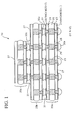
- FIG. 1 schematically shows the sectional structure of a semiconductor device according to an embodiment of the present invention.
- the semiconductor device 10 has a three-dimensionally mounted configuration formed by stacking structures 20a, 20b, 20c in three stages, as shown in the figure.
- numerals 21 and 22 denote a silicon substrate thinned to a prescribed thickness, respectively
- numerals 23 and 24 denote a conductor layer which is formed on one surface of the corresponding silicon substrate 21, 22, respectively, and which involves device patterns including required circuit patterns, wiring patterns, or the like
- the numeral 25 denotes a metal bump which bonds the two silicon substrates 21, 22 through each of the conductor layers 23, 24 as will be described later
- numeral 26 denotes an insulative resin layer formed by being filled into a gap between the conductor layers 23, 24 bonded together by means of the metal bump 25.
- the metal bump 25 functions as a metal post
- the insulative resin layer 26 functions as a buffer layer to cushion mechanical shocks caused by the thinning treatment of a silicon substrate as will be described later, and also functions as a reinforc
- the conductor 28 is electrically connected to the metal bump 25 through an opening (indicated by OP in FIG. 2F) formed in part of the insulating film 27 within the via hole. Therefore, the electrode pads 29 formed on both surfaces of each of the structures 20a, 20b, 20c are interconnected through the conductor 28 and the metal bump 25.
- each of the structures 20a, 20b, 20c is selected to be approximately 50 ⁇ m; the thickness (t1, t2) of the thinned silicon substrates 21, 22 is selected to be in the range of 3 to 20 ⁇ m; and the thickness of the insulative resin layer (buffer layer) 26 is selected to be approximately 30 ⁇ m.
- numerals 30a, 30b and 30c denote a metal bump bonded to the electrode pad 29 on the side of one surface (lower side in the illustrated example) of the corresponding structures 20a, 20b, 20c.
- the metal bump 30a bonded to the electrode pad 29 of the lowest-positioned structure 20a functions as an external terminal of this device 10.
- numeral 31 denotes an insulative resin layer filled as an underfill into gaps between the stacked structures 20a, 20b, 20c.
- Pb-free solders such as silver-tin (Ag-Sn) are used, in addition to eutectic solders, such as generally-used lead-tin (Pb-Sn).
- gold (Au), silver (Ag), copper (Cu), indium (In) or its alloys (In-Pb, In-Sn, or the like), nickel (Ni), and the like may be used.
- each of the bumps 25, 30a, 30b and 30c may be formed by a generally-used plating method utilizing photo processes, or may be a ball bump such as a stud bump formed by means of wire bonding techniques.
- Cu is typically used as the material for the device patterns (conductor layers 23, 24) including circuit patterns and wiring patterns.
- Au, Cu, Ni, chromium (Cr), aluminum (Al), or the like, is used as the material for the conductor 28 and the electrode pad 29.
- epoxy resin, polyimide resin, or the like is used as the material for the insulative resin layer (buffer layer) 26 and the insulative resin layer (underfill material) 31.
- photosensitive resin such as polyimide resin, epoxy resin, or the like, silicon oxide films formed by chemical vapor deposition (CVD) process, phosphorous silicate glass (PSG), or the like, is used.
- the external connection terminal (metal bump 30a) is provided as shown in FIG. 1, it is not always necessary to provide the external connection terminal. This is because such an external connection terminal may be provided immediately before the semiconductor device 10 is mounted on a mother board such as a printed circuit board, in actual use. Therefore, as a final configuration of the semiconductor device 10, it is necessary only that the electrode pad 29 be exposed so that the external connection terminal (metal bump 30a) can be bonded.
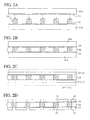
- FIG. 2A to FIG. 2K show the manufacturing steps in sequence.
- two silicon substrates 21a and 22a, on respective one-side surfaces of which a conductor layer 23, 24 patterned to a required shape is formed, are bonded by means of a metal bump 25, while the respective one-side surfaces on which the conductor layer 23, 24 is formed face each other.
- two relatively thick silicon substrates 21a, 22a having a thickness of approximately 100 ⁇ m to 300 ⁇ m are first prepared, and on respective one-side surfaces of the silicon substrates 21a, 22a are formed required device patterns (conductor layers 23, 24), by means of a well-known photolithography technique.
- a plurality of metal bumps 25 are bonded to prescribed positions on the conductor layer 23 of one silicon substrate 21a, for example, by ultrasonic bonding (i.e., bonding method which utilizes the thermal action or cavitation effect of ultrasonic waves), thermocompression bonding (wire bonding method, reflow soldering method), or the like.
- the two silicon substrates 21a, 22a are bonded together through the conductor layers 23, 24 by means of the metal bump 25, while the one-side surface to which the metal bump 25 of this silicon substrate 21a is bonded is faced with the one-side surface on which the conductor layer 24 of the other silicon substrate 22a is formed. Namely, a structure in which the two silicon substrates 21a, 22a are stuck together through the metal bump 25 is obtained.
- the structure obtained in the preceding step (formed by sticking the two silicon substrates 21a, 21b together through the metal bump 25) is placed in a vacuum chamber and an insulative resin such as epoxy resin is then filled into a gap between the conductor layers 23, 24 bonded by the metal bump 25, to thereby form an insulative resin layer 26 having a thickness of approximately 30 ⁇ m.
- both surfaces of the structure obtained in the preceding step i.e., the surfaces of the exposed sides of the silicon substrate 21a, 22a, are thinned by performing mechanical polishing such as a back-grinding method, so as to constitute silicon substrates 21, 22 having a thickness (t1 ⁇ t2) of approximately 3 ⁇ m to 20 ⁇ m.
- the portions indicated by broken lines in the figure represent portions removed by the polishing.
- a via hole VH reaching the metal bump 25 is formed in a required place of each of the semiconductor substrates 21, 22 thinned in the preceding step.
- the via hole VH can be formed by drilling, for example, by means of a CO 2 laser, a YAG laser, an excimer laser, or the like, or by etching, for example, by means of a plasma etcher.
- a silicon oxide film (SiO 2 ), i.e., an insulating film 27, is formed on the surface of the silicon substrates 21, 22 including the inner surface of the via hole VH formed therein.
- the insulating film 27 is formed to electrically insulate a conductor layer to be filled in the via hole VH in a subsequent step from the silicon substrates 21, 22, and also functions as a protective film as described above.
- a silicon oxide film is formed as the insulating film 27, for example, a phosphorus silicate glass (PSG) may be formed by means of CVD method, in place of the silicon oxide film.
- a resin in particular, a photosensitive resin
- polyimide resin epoxy resin, or the like
- opening OP can be formed, by the same treatment as in the step of FIG. 2D, i.e., by drilling, for example, by means of a CO 2 laser, a YAG laser, or the like, or by etching, for example, by means of a plasma etcher.
- the opening OP of the insulating film 27 is formed by a laser, plasma etching, or the like, where the insulating film 27 is formed by coating a photosensitive resin, it is also possible to form the opening OP by a well-known photolithography technique.
- a conductor layer CL is formed to fill the via hole VH formed in each of the silicon substrates 21, 22 (part of the insulating film 27 formed therein opens (opening OP)).
- the whole surface is first subjected to electroless nickel (Ni)plating, and then, the nickel layer is subjected to electroless gold (Au)plating, or to flash plating (plating of very small thickness) by electrolytic Au plating using the Ni layer as a power supply layer.
- electrolytic copper (Cu) plating is performed to fill the via hole VH using the Au layer as a power supply layer, to thereby form a three-layer (Ni/Au/Cu) conductor layer CL.
- the Ni layer in the conductor layer CL is intended to increase the adhesion to the underlying insulating film (SiO 2 ) 27, and the Au layer is formed to lower electrical resistance during electrolytic Cu plating.
- a conductor 28 buried in the via hole VH is used to form an electrode pad on this conductor in a subsequent step. Also, since the treatment which is little more than plating is performed in this step, a conductor layer 28a is formed as shown in the figure also in portions other than the via hole VH on the insulating film 27.
- the whole surface is made flat by removing the unnecessary conductor layer 28a formed in portions other than the via hole VH on the insulating film 27 by means of mechanical polishing, chemical mechanical polishing (CMP), or the like, until the top end surface of the conductor 28 buried in the via hole VH on the insulating film 27 is exposed.
- CMP chemical mechanical polishing
- each of the insulating films 27 on both sides is formed an electrode pad 29 of a required shape, so as to be electrically connected to the conductor 28 buried in the via hole VH.
- the electrode pad 29 can be formed, for example, by coating or forming a resist (not shown) on the whole surface, patterning the resist to a required shape, and performing a sputtering of Cu, Al, Au, Cr, or the like, by means of the resist as a mask. Alternatively, any plating may be performed in place of the sputtering.
- each of the structures 20a, 20b, 20c which constitute the semiconductor device 10 is fabricated.
- the structure 20a of the lowest stage is shown, the other structures 20b, 20c can also be similarly fabricated by the steps shown in FIG. 2A to FIG. 21.
- the structures 20b, 20c differ from the structure 20a in that the position where the via hole VH is formed in the step of FIG. 2D is different from that of the structure 20a.
- a metal bump 30a is bonded to the electrode pad 29 on the lower side of the structure 20a formed in the preceding step.
- metal bumps 30b, 30c are also similarly bonded to the other structures 20b, 20c. In this case, as described above, it is not always necessary to provide the metal bump 30a on the structure 20a of the lowest stage.
- Solder, Au, Ag, In, or the like is used as the material for the metal bumps 30a, 30b, 30c.
- In because of the considerably low melting point of this metal compared with other metals, there is a merit in that, in performing bump bonding, it is possible to suppress a thermal effect on the resin layer (in this case, the insulative resin layer 26) in the structure.
- the structures 20a, 20b, 20c to which the metal bumps 30a, 30b, 30c are bonded, respectively, are stacked and electrically interconnected by thermocompression bonding, or the like, through the metal bumps 30b, 30c.
- the metal bump 30a of the structure 20a of the lowest stage is used as an external connection terminal.
- an insulative resin as an underfill is filled into the gap between the stacked structures 20a, 20b, 20c, whereby the semiconductor device 10 (FIG. 1) of this embodiment is obtained.
- the buffer layer 26 is interposed between the facing conductor layers 23, 24 of the silicon substrates 21a, 22a, it is possible to effectively absorb and buffer mechanical shocks caused by the polishing of each substrate, with the aid of the buffer layer 26. This contributes to an improvement in the crack resistance of the silicon substrates 21, 22. In other words, even if the silicon substrates are thinned to a level close to the limit of the state-of-the art, it is possible to eliminate drawbacks as seen in previously-proposed methods, such as occurrence of cracks, damage to a substrate, or the like.
- the polishing is conducted on a structure obtained by sticking the two silicon structures 21a, 22a together symmetrically as if reflected in a mirror, while the respective one-side surfaces on which the device pattern (the conductor layer 23, 24) is formed face each other, it is possible to eliminate drawbacks as seen in previously-proposed methods, such as a warping of the silicon substrate caused by a difference in stress generated between the one surface and another surface of the substrate.
- each of the silicon substrates 21, 22 is reduced to approximately 3 ⁇ m to 20 ⁇ m, it becomes easy to form the via hole VH in the thinned silicon substrates (FIG. 2C, FIG. 2D).
- the explanation is made with respect to the case where the conductor layer CL of Ni/Au/Cu is formed by means of electroless plating and electrolytic plating in the step of FIG. 2G.
- the method of forming the conductor layer CL is not limited to the above case.
- a required film may be formed by sputtering, in place of the electroless plating.
- Cr for example, is deposited by sputtering on the whole surface of each insulating layer 27 including the inner surface of the via hole VH and the surface of the exposed metal bump 25; Cu is further deposited on the Cr layer by sputtering, so as to form a metal thin film of two-layer structure; and a metal layer of Cu is formed on the entire surface by electrolytic plating, by means of the metal thin film as a power supply layer, whereby it is possible to form a conductor layer of Cr/Cu.
- the Cr layer which is the underlayer portion of the metal thin layer is formed to increase adhesion to the underlying insulating film 27.
- the explanation is made with respect to the case where the structures 20a, 20b, 20c are stacked in three stages by aligning the positions of the metal bumps 25 and the electrode pads 29 of each structure.
- FIG. 3 An example of such a single-stage structure is shown in FIG. 3.
- FIG. 3 schematically shows the sectional structure of a semiconductor device according to another embodiment of the present invention.
- the semiconductor device 40 according to this embodiment differs from the semiconductor device 10 according to the above-described embodiment (FIG. 1 and FIG. 2A to FIG. 2K) in that the structure (equivalent to each of the structures 20a, 20b, 20c shown in FIG. 2K) is not stacked in multiple stages, and in that, in polishing each of the silicon substrates 42a, 42b from both sides as will be described later, only one silicon substrate is thinned to a prescribed thickness (T1), while the thickness of the other silicon substrate is not reduced so as to have a certain thickness (T2). Since the other features are basically the same as those of the structure 20c of the highest stage shown in Fig. 1, the description thereof is omitted.
- FIG. 4A to FIG. 4G show the manufacturing steps in sequence.
- two silicon substrates 41a, 42a are bonded together by means of a metal bump 45, while respective one-side surfaces on which a conductor layer 43, 44 (device pattern) is formed face each other, and an insulative resin 46 as a buffer layer is filled into a gap between the surfaces.
- both surfaces of the structure obtained in the preceding step are polished by means of a back grinding method in such a manner that only one silicon substrate 41a is thinned to a prescribed thickness T1 (approximately 3 ⁇ m to 20 ⁇ m) to thereby obtain a silicon substrate 41, while for the other silicon substrate 42a, the amount of polishing is relatively reduced to have a certain thickness T2 (approximately 100 ⁇ m to 300 ⁇ m) to thereby obtain a silicon substrate 42.
- T1 approximately 3 ⁇ m to 20 ⁇ m
- T2 approximately 100 ⁇ m to 300 ⁇ m
- a via hole VH which reaches the metal bump 45 is formed in a required place of one semiconductor substrate 41 thinned in the preceding step.
- the via hole VH can be formed by drilling, for example, by means of a laser, or by etching, for example, by means of a plasma etcher.
- an insulating film 47 such as a silicon oxide film is formed by means of a CVD process, for example, on the surface of each of the silicon substrates 41, 42 including the inner surface of the via hole VH. Furthermore, by means of a laser or a plasma etcher, for example, at least part of the portion in contact with the metal bump 45, of the insulating film 47 formed in the via hole VH, is opened (opening OP). As a result, part of the metal bump 45 is exposed.
- a conductor layer is formed by plating, for example, so as to fill the via hole VH formed in one silicon substrate 41(part of the insulating film 47 formed therein opens (opening OP)), and a conductor 48 embedded in the via hole VH is formed by removing the unnecessary conductor layer formed in portions other than the via hole VH, by means of mechanical polishing, or the like.
- an electrode pad 49 of a required shape is formed on the insulating film 47 on one silicon substrate 41 in the next step (FIG. 4F).
- the electrode pad 49 can be formed by sputtering, plating, or the like, in the same manner as in the treatment performed in the above-described step of FIG. 21.
- the insulative layer (the buffer layer) 46 it is possible to effectively absorb and buffer mechanical shocks caused by the polishing of each of the substrates 41a, 42a, and hence it is possible to eliminate drawbacks such as occurrence of cracks, or the like, in the silicon substrates 41, 42. Furthermore, since the polishing is conducted on a structure obtained by sticking the two silicon structures 41a, 42a together symmetrically as if reflected in a mirror, while the respective one-side surfaces on which the device pattern (the conductor layer 43, 44) is formed face each other, it is possible to eliminate drawbacks such as a warping of the silicon substrate caused by a difference in stress generated between the two surfaces. Similarly, since the thickness of the silicon substrate 41 is reduced to approximately 3 ⁇ m to 20 ⁇ m, it becomes easy to form the via hole VH in the thinned silicon substrates (FIG. 4B, FIG. 4C).
Landscapes
- Internal Circuitry In Semiconductor Integrated Circuit Devices (AREA)
- Production Of Multi-Layered Print Wiring Board (AREA)
- Wire Bonding (AREA)
- Combinations Of Printed Boards (AREA)
Abstract
Description
- The present invention relates to a semiconductor device and its manufacturing method and, more particularly, to a technique adapted to eliminate drawbacks arising in association with a thinning in performing three-dimensional mounting intended for the high density design and multiple-pin design of semiconductor devices.
- Various methods have been previously proposed as techniques for accomplishing the high density design and multiple-pin design of semiconductor devices. One available method, for example, involves fabricating a printed wiring board of multilayer structure by means of a build-up method and mounting elements such as semiconductor chips on the multilayer printed wiring board so as to obtain a device.
- Also, in another available method, instead of fabricating a printed wiring board of multilayer structure, a printed wiring board is fabricated by forming wiring patterns on both sides of one insulative substrate, fabricating a device by mounting elements such as semiconductor chips on the wiring patterns of one surface of the printed wiring board, and performing three-dimensional mounting by stacking such devices. According to this method, it is necessary to electrically interconnect the respective semiconductor chips mounted on each of the printed wiring boards. To this end, through holes are formed in each of the printed wiring boards by piercing the printed wiring board, and wiring patterns formed on both surfaces of the printed wiring board are electrically interconnected through plated films (conductor layers) formed on the inner surfaces of the through holes.
- Also, as still another method of performing three-dimensional mounting, there is a conceivable method which involves: using a silicon (Si) substrate as a base material layer; forming a hole with a required depth in the silicon substrate; forming required device patterns (including circuit patterns, wiring patterns, or the like) after filling the hole with a conductor by plating, or the like, so that the device patterns are electrically connected to the conductor; covering the device patterns with insulating films formed of polyimide resin, or the like; exposing the conductor by polishing the back surface of the silicon substrate by means of a back-grinding method, or the like; fabricating a device by providing metal bumps (external connection terminals) on the exposed conductor; and stacking a required number of devices.
- Likewise in this method, it is necessary to electrically interconnect each of the devices, and to this end, it is necessary to form through holes in the insulating film of the device, plate the inner surfaces of the through holes, and electrically connect device patterns via the plated film to metal bumps of an upper-positioned device.
- As described above, various techniques have been proposed as techniques for accomplishing the high density design and multiple-pin design of semiconductor devices. Among these, in the technique utilizing a build-up method, the thickness of the printed wiring board is considerably increased because the printed wiring board is fabricated to have a multilayer structure. Accordingly, the scale of the whole semiconductor device in final form becomes large, resulting in a problem in that it is not possible to fully meet the recent requirement for thinning design.
- Also, the method which involves forming a device by means of an insulative substrate and stacking a required number of devices, is favorable in terms of the high density design and multiple-pin design, compared with the above technique utilizing a build-up method, because a plurality of semiconductor chips are mutually three-dimensionally mounted. However, this method has a drawback in terms of the thinning design in the same manner as described above, because semiconductor chips are interposed between printed wiring boards.
- On the other hand, the method which involves forming a device by means of a silicon substrate and stacking a required number of devices, is favorable in terms of the thinning design, because the thickness of the silicon substrate is reduced by polishing the back surface thereof. However, this method poses the following problems:
- Namely, in this method, a mechanical polishing such as a back-grinding method is performed to make the silicon substrate thin, and accordingly, there is a limit to the thickness of the silicon substrate to be thinned due to mechanical shocks of the mechanical polishing. If the silicon substrate is made excessively thin, a problem would arise in that cracks occur in the silicon substrate and, in some cases, the silicon substrate may be broken or damaged.
- Also, the surface on one side of the silicon substrate, on which device patterns are formed, is formed of an insulating film of polyimide resin, or the like, while the surface on another side is formed of a conductor. Namely, the two surfaces have different coefficients of thermal expansion, which causes a difference in stress to be generated between the one surface and another surface. As a result, for example, when polishing treatment is performed, a problem arises in that the silicon substrate is warped.
- Accordingly it is desirable to provide a semiconductor device and its manufacturing method, which can eliminate drawbacks arising in association with a thinning (damage to a semiconductor substrate, occurrence of cracks, warping of a semiconductor substrate, or the like) in performing three-dimensional mounting intended for the high density design and multiple-pin design.
- According to an embodiment of one aspect of the present invention, there is provided a method of manufacturing a semiconductor device, which includes the steps of: bonding, by means of a metal bump, two semiconductor substrates, on respective one-side surfaces of which a conductor layer patterned to a required shape is formed, while facing the respective one-side surfaces to each other; filling, with an insulating resin, a gap between the respective conductor layers bonded by means of the metal bump; polishing each of exposed side surfaces of the semiconductor substrates to thereby thin each of the semiconductor substrates to a prescribed thickness; forming a via hole which reaches the metal bump, in a required place of each of the thinned semiconductor substrates; forming an insulating film on the surface of each of the semiconductor substrates including an inner surface of the formed via hole; opening at least part of a portion in contact with the metal bump, of the insulating film formed within the via hole; filling an inside of the via hole with a conductor and further forming, on the insulating film, an electrode pad patterned to a required shape and electrically connected to the conductor; and stacking a structure obtained by the above-described steps, by a required number, by electrically connecting respective structures with each other through the electrode pad.
- According to an embodiment of this aspect of the present invention, it is possible to accomplish a thinning design as the whole semiconductor device in a three-dimensionally mounted configuration which is finally manufactured, because two semiconductor substrates are first bonded together by means of a metal bump, while respective one-side surfaces, on which conductor layers (device patterns) are formed, face each other, and an insulating resin is then filled into the gaps between the semiconductor substrates, and thereafter the thickness of each of the substrates is reduced by polishing both surfaces, i.e., each of the exposed side surfaces of the semiconductor substrates.
- Also, since the insulating resin is filled into the gap between the facing conductor layers of the semiconductor substrates, it is possible to effectively absorb and buffer mechanical shocks caused by the polishing (thinning treatment)of each substrate, with the aid of the insulating resin. Namely, the insulating resin-functions as a cushion (a buffer layer). As a result, even in the case that semiconductor substrates are thinned to a level close to the limit of the state-of-the art, it is possible to eliminate drawbacks as seen in previously-proposed methods, such as the occurrence of cracks and damage to a substrate. In other words, it is possible to improve the crack resistance of the semiconductor substrate.
- Furthermore, since polishing (thinning treatment) is conducted on a structure obtained by sticking the two semiconductor structures together symmetrically as if reflected in a mirror, while the respective one-side surfaces, on which the conductor layers (device patterns) are formed, face each other, it is possible to eliminate drawbacks as seen in previously-proposed methods, such as warping of a semiconductor substrate caused by a difference in stress generated between the one surface and another surface of the substrate. In other words, it is possible to remedy the warping of the semiconductor substrate.
- Also, according to an embodiment of another aspect of the present invention, there is provided a method of manufacturing a semiconductor device, which includes the steps of: bonding, by means of a metal bump, two semiconductor substrates, on respective one-side surfaces of which a conductor layer patterned to a required shape is formed, while facing the respective one-side surfaces to each other; filling, with an insulating resin, a gap between the respective conductor layers bonded by means of the metal bump; polishing each of exposed side surfaces of the semiconductor substrates to thereby thin only one of the semiconductor substrates to a prescribed thickness; forming a via hole which reaches the metal bump, in a required place of the thinned semiconductor substrate; forming an insulating film on the surface of each of the semiconductor substrates including an inner surface of the formed via hole; opening at least part of a portion in contact with the metal bump, of the insulating film formed within the via hole; and filling an inside of the via hole with a conductor and further forming, on the insulating film on the thinned semiconductor substrate, an electrode pad patterned to a required shape and electrically connected to the conductor.
- According to an embodiment of this aspect, in the same manner as in an embodiment of the above-described aspect, it is possible to accomplish a thinning design as the whole semiconductor device in a three-dimensionally mounted configuration which is finally manufactured, because two semiconductor substrates are first bonded together by means of a metal bump, while respective one-side surfaces on which conductor layers (device patterns) are formed face each other, and an insulating resin is then filled into the gaps between the silicon substrates, and thereafter the thickness of one of the substrates is reduced to a prescribed thickness when polishing each exposed surface of the silicon substrates. Also, owing to the presence of the insulating resin which functions as a buffer layer, it is possible to buffer mechanical shocks caused by the polishing (thinning treatment), and thus to eliminate drawbacks such as the occurrence of cracks in the semiconductor substrate. Furthermore, since polishing (thinning treatment) is conducted on a structure obtained by sticking the two semiconductor structures together symmetrically as if reflected in a mirror, while the respective one-side surfaces on which the conductor layers (device patterns) are formed face each other, it is possible to eliminate drawbacks, such as warping of a semiconductor substrate caused by a difference in stress generated between the one surface and another surface of the substrate.
- Also, according to an embodiment of still another aspect of the present invention, there is provided a semiconductor device manufactured by a method embodying the present invention.
- Reference will now be made, by way of example, to the accompanying drawings, in which:
- FIG. 1 is a sectional view showing the structure of a semiconductor device according to an embodiment of the present invention;
- FIG. 2A to FIG. 2K are sectional views showing the manufacturing steps of the semiconductor device shown in FIG. 1;
- FIG. 3 is a sectional view showing the structure of a semiconductor device according to another embodiment of the present invention; and
- FIG. 4A to FIG. 4G are sectional views showing the manufacturing steps of the semiconductor device shown in FIG. 3.
-
- FIG. 1 schematically shows the sectional structure of a semiconductor device according to an embodiment of the present invention.
- The
semiconductor device 10 according to this embodiment has a three-dimensionally mounted configuration formed bystacking structures structures numerals numerals corresponding silicon substrate numeral 25 denotes a metal bump which bonds the twosilicon substrates conductor layers numeral 26 denotes an insulative resin layer formed by being filled into a gap between theconductor layers metal bump 25. Themetal bump 25 functions as a metal post, and theinsulative resin layer 26 functions as a buffer layer to cushion mechanical shocks caused by the thinning treatment of a silicon substrate as will be described later, and also functions as a reinforcing agent. - Also,
numeral 27 denotes an insulating film which functions as a protective film for each of thestructures numeral 28 denotes a conductor filled into a via hole formed in each of thesilicon substrates numeral 29 denotes an electrode pad formed on each of theinsulating films 27 and electrically connected to theconductor 28. Theconductor 28 is electrically connected to themetal bump 25 through an opening (indicated by OP in FIG. 2F) formed in part of theinsulating film 27 within the via hole. Therefore, theelectrode pads 29 formed on both surfaces of each of thestructures conductor 28 and themetal bump 25. - The thickness of each of the
structures thinned silicon substrates - Also,
numerals electrode pad 29 on the side of one surface (lower side in the illustrated example) of thecorresponding structures metal bump 30a bonded to theelectrode pad 29 of the lowest-positionedstructure 20a functions as an external terminal of thisdevice 10. Also,numeral 31 denotes an insulative resin layer filled as an underfill into gaps between thestacked structures - In the above-described structure, as the materials which constitute the
metal bumps bumps - Also, Cu is typically used as the material for the device patterns (
conductor layers 23, 24) including circuit patterns and wiring patterns. In order to further increase electrical conductivity and improve the reliability of connection to themetal bump 25, it is preferable to apply a coating of Au, Sn, or the like, for example. Furthermore, Au, Cu, Ni, chromium (Cr), aluminum (Al), or the like, is used as the material for theconductor 28 and theelectrode pad 29. Also, epoxy resin, polyimide resin, or the like is used as the material for the insulative resin layer (buffer layer) 26 and the insulative resin layer (underfill material) 31. Furthermore, as the material for the insulating film (protective film) 27, photosensitive resin such as polyimide resin, epoxy resin, or the like, silicon oxide films formed by chemical vapor deposition (CVD) process, phosphorous silicate glass (PSG), or the like, is used. - Although in this embodiment the external connection terminal (
metal bump 30a) is provided as shown in FIG. 1, it is not always necessary to provide the external connection terminal. This is because such an external connection terminal may be provided immediately before thesemiconductor device 10 is mounted on a mother board such as a printed circuit board, in actual use. Therefore, as a final configuration of thesemiconductor device 10, it is necessary only that theelectrode pad 29 be exposed so that the external connection terminal (metal bump 30a) can be bonded. - Hereinafter, a method of manufacturing the
semiconductor device 10 according to the present embodiment will be described with reference to FIG. 2A to FIG. 2K which show the manufacturing steps in sequence. - First, in the first step (FIG. 2A), two
silicon substrates conductor layer metal bump 25, while the respective one-side surfaces on which theconductor layer - Specifically, two relatively
thick silicon substrates silicon substrates metal bumps 25 are bonded to prescribed positions on theconductor layer 23 of onesilicon substrate 21a, for example, by ultrasonic bonding (i.e., bonding method which utilizes the thermal action or cavitation effect of ultrasonic waves), thermocompression bonding (wire bonding method, reflow soldering method), or the like. Subsequently, the twosilicon substrates metal bump 25, while the one-side surface to which themetal bump 25 of thissilicon substrate 21a is bonded is faced with the one-side surface on which theconductor layer 24 of theother silicon substrate 22a is formed. Namely, a structure in which the twosilicon substrates metal bump 25 is obtained. - In the next step (FIG. 2B), the structure obtained in the preceding step (formed by sticking the two
silicon substrates 21a, 21b together through the metal bump 25) is placed in a vacuum chamber and an insulative resin such as epoxy resin is then filled into a gap between the conductor layers 23, 24 bonded by themetal bump 25, to thereby form aninsulative resin layer 26 having a thickness of approximately 30 µm. - In the next step (FIG. 2C), both surfaces of the structure obtained in the preceding step, i.e., the surfaces of the exposed sides of the
silicon substrate silicon substrates - In the next step (FIG. 2D), a via hole VH reaching the
metal bump 25 is formed in a required place of each of thesemiconductor substrates - In the next step (FIG. 2E), by means of a CVD process, a silicon oxide film (SiO2), i.e., an insulating
film 27, is formed on the surface of thesilicon substrates - The insulating
film 27 is formed to electrically insulate a conductor layer to be filled in the via hole VH in a subsequent step from thesilicon substrates - Although in this step a silicon oxide film is formed as the insulating
film 27, for example, a phosphorus silicate glass (PSG) may be formed by means of CVD method, in place of the silicon oxide film. Alternatively, it is also possible to form the insulatingfilm 27 by coating a resin (in particular, a photosensitive resin), such as polyimide resin, epoxy resin, or the like, on the whole surface. - In the next step (FIG. 2F), among the respective insulating
films 27 on both surfaces formed in the preceding step, at least part of a portion in contact with themetal bump 25, of the insulatingfilm 27 formed within the via hole VH, is opened (opening OP). The opening OP can be formed, by the same treatment as in the step of FIG. 2D, i.e., by drilling, for example, by means of a CO2 laser, a YAG laser, or the like, or by etching, for example, by means of a plasma etcher. - As a result, a portion corresponding to the opening OP of the insulating
film 27 in the via hole VH, i.e., part of themetal bump 25 is exposed. - Although in this step, the opening OP of the insulating
film 27 is formed by a laser, plasma etching, or the like, where the insulatingfilm 27 is formed by coating a photosensitive resin, it is also possible to form the opening OP by a well-known photolithography technique. - In the next step (FIG. 2G), by means of electroless plating or electrolytic plating, for example, a conductor layer CL is formed to fill the via hole VH formed in each of the
silicon substrates 21, 22 (part of the insulatingfilm 27 formed therein opens (opening OP)). - Specifically, the whole surface is first subjected to electroless nickel (Ni)plating, and then, the nickel layer is subjected to electroless gold (Au)plating, or to flash plating (plating of very small thickness) by electrolytic Au plating using the Ni layer as a power supply layer. Subsequently, electrolytic copper (Cu) plating is performed to fill the via hole VH using the Au layer as a power supply layer, to thereby form a three-layer (Ni/Au/Cu) conductor layer CL. The Ni layer in the conductor layer CL is intended to increase the adhesion to the underlying insulating film (SiO2) 27, and the Au layer is formed to lower electrical resistance during electrolytic Cu plating.
- In the conductor layer CL thus formed, a
conductor 28 buried in the via hole VH is used to form an electrode pad on this conductor in a subsequent step. Also, since the treatment which is little more than plating is performed in this step, aconductor layer 28a is formed as shown in the figure also in portions other than the via hole VH on the insulatingfilm 27. - In the next step (FIG. 2H), the whole surface is made flat by removing the
unnecessary conductor layer 28a formed in portions other than the via hole VH on the insulatingfilm 27 by means of mechanical polishing, chemical mechanical polishing (CMP), or the like, until the top end surface of theconductor 28 buried in the via hole VH on the insulatingfilm 27 is exposed. - In the next step (FIG. 21), on each of the insulating
films 27 on both sides is formed anelectrode pad 29 of a required shape, so as to be electrically connected to theconductor 28 buried in the via hole VH. - The
electrode pad 29 can be formed, for example, by coating or forming a resist (not shown) on the whole surface, patterning the resist to a required shape, and performing a sputtering of Cu, Al, Au, Cr, or the like, by means of the resist as a mask. Alternatively, any plating may be performed in place of the sputtering. - As a result of the above-described steps, each of the
structures semiconductor device 10 is fabricated. Although in the example of FIG. 21, thestructure 20a of the lowest stage is shown, theother structures structures structure 20a in that the position where the via hole VH is formed in the step of FIG. 2D is different from that of thestructure 20a. - In the next step (FIG. 2J), a
metal bump 30a is bonded to theelectrode pad 29 on the lower side of thestructure 20a formed in the preceding step. Although not shown in the figure, metal bumps 30b, 30c are also similarly bonded to theother structures metal bump 30a on thestructure 20a of the lowest stage. - Solder, Au, Ag, In, or the like, is used as the material for the
metal bumps - In the final step (FIG. 2K), the
structures metal bumps metal bump 30a of thestructure 20a of the lowest stage is used as an external connection terminal. - Furthermore, an insulative resin as an underfill is filled into the gap between the
stacked structures - As described above, according to the semiconductor device 10 (FIG. 1) of this embodiment and its manufacturing method (FIG. 2A to FIG. 2K), it is possible to accomplish a thinning design as the
whole semiconductor device 10 in a three-dimensionally mounted configuration to be finally manufactured, because thesilicon substrates metal bump 25, while the respective one-side surfaces on which the device pattern (theconductor layer 23, 24) is formed face each other; the insulative resin (buffer layer) 26 is filled into the gap between thesilicon substrates silicon substrates silicon substrates 21, 22). - Also, since the
buffer layer 26 is interposed between the facing conductor layers 23, 24 of thesilicon substrates buffer layer 26. This contributes to an improvement in the crack resistance of thesilicon substrates - Furthermore, since the polishing is conducted on a structure obtained by sticking the two
silicon structures conductor layer 23, 24) is formed face each other, it is possible to eliminate drawbacks as seen in previously-proposed methods, such as a warping of the silicon substrate caused by a difference in stress generated between the one surface and another surface of the substrate. - Furthermore, since the thickness of each of the
silicon substrates - In the above-described embodiment, the explanation is made with respect to the case where the conductor layer CL of Ni/Au/Cu is formed by means of electroless plating and electrolytic plating in the step of FIG. 2G. However, the method of forming the conductor layer CL is not limited to the above case. For example, a required film may be formed by sputtering, in place of the electroless plating.
- As a specific example, Cr, for example, is deposited by sputtering on the whole surface of each insulating
layer 27 including the inner surface of the via hole VH and the surface of the exposedmetal bump 25; Cu is further deposited on the Cr layer by sputtering, so as to form a metal thin film of two-layer structure; and a metal layer of Cu is formed on the entire surface by electrolytic plating, by means of the metal thin film as a power supply layer, whereby it is possible to form a conductor layer of Cr/Cu. In this case, as with the Ni layer in the above-described conductor layer CL, the Cr layer which is the underlayer portion of the metal thin layer is formed to increase adhesion to the underlying insulatingfilm 27. - Also, in the above-described embodiment, the explanation is made with respect to the case where the
structures electrode pads 29 of each structure. However, as a matter of course, it is not always necessary to align the positions of the metal bumps 25 and the positions of the electrode pads 29 (i.e., the positions of themetal bumps - Also, it is not always necessary to stack such a structure in multiple stages, and the structure may be made in a single stage depending on the required conditions. An example of such a single-stage structure is shown in FIG. 3.
- FIG. 3 schematically shows the sectional structure of a semiconductor device according to another embodiment of the present invention.
- The
semiconductor device 40 according to this embodiment differs from thesemiconductor device 10 according to the above-described embodiment (FIG. 1 and FIG. 2A to FIG. 2K) in that the structure (equivalent to each of thestructures silicon substrates 42a, 42b from both sides as will be described later, only one silicon substrate is thinned to a prescribed thickness (T1), while the thickness of the other silicon substrate is not reduced so as to have a certain thickness (T2). Since the other features are basically the same as those of thestructure 20c of the highest stage shown in Fig. 1, the description thereof is omitted. - Hereinafter, a method of manufacturing the
semiconductor device 40 according to this embodiment will be described with reference to FIG. 4A to FIG. 4G which show the manufacturing steps in sequence. - First, in the first step (FIG. 4A), in the same manner as with the treatment performed in the steps of FIG. 2A and FIG. 2B, two
silicon substrates metal bump 45, while respective one-side surfaces on which aconductor layer 43, 44 (device pattern) is formed face each other, and aninsulative resin 46 as a buffer layer is filled into a gap between the surfaces. - In the next step (FIG. 4B), both surfaces of the structure obtained in the preceding step (i.e., respective one-side surfaces to which the
silicon substrate silicon substrate 41a is thinned to a prescribed thickness T1 (approximately 3 µm to 20 µm) to thereby obtain asilicon substrate 41, while for theother silicon substrate 42a, the amount of polishing is relatively reduced to have a certain thickness T2 (approximately 100 µm to 300 µm) to thereby obtain asilicon substrate 42. The portions indicated by broken lines in the figure represent portions removed by the polishing. - In the next step (FIG. 4C), a via hole VH which reaches the
metal bump 45 is formed in a required place of onesemiconductor substrate 41 thinned in the preceding step. In the same manner as in the treatment performed in the above-described step of FIG. 2D, the via hole VH can be formed by drilling, for example, by means of a laser, or by etching, for example, by means of a plasma etcher. - In the next step (FIG. 4D), in the same manner as in the treatment performed in the above-described steps of FIG. 2E and FIG. 2F, an insulating
film 47 such as a silicon oxide film is formed by means of a CVD process, for example, on the surface of each of thesilicon substrates metal bump 45, of the insulatingfilm 47 formed in the via hole VH, is opened (opening OP). As a result, part of themetal bump 45 is exposed. - In the next step (FIG. 4E), in the same manner as in the treatment performed in the above-described steps of FIG. 2G and FIG. 2H, a conductor layer is formed by plating, for example, so as to fill the via hole VH formed in one silicon substrate 41(part of the insulating
film 47 formed therein opens (opening OP)), and aconductor 48 embedded in the via hole VH is formed by removing the unnecessary conductor layer formed in portions other than the via hole VH, by means of mechanical polishing, or the like. - In the next step (FIG. 4F), on the insulating
film 47 on onesilicon substrate 41 is formed anelectrode pad 49 of a required shape, so as to be electrically connected to theconductor 48 embedded in the via hole VH. Theelectrode pad 49 can be formed by sputtering, plating, or the like, in the same manner as in the treatment performed in the above-described step of FIG. 21. - In the final step (FIG. 4G), a
metal bump 50 as an external connection terminal is bonded to theelectrode pad 49 formed in the preceding step. As a result, the semiconductor device 40 (FIG. 3) of this embodiment is obtained. - According to the embodiment shown in FIG. 3 and FIG. 4A to FIG. 4G, as in the case of the above-described embodiment (FIG. 1 and FIG. 2A to FIG. 2K), it is possible to accomplish a thinning design as the
whole semiconductor device 40 to be finally manufactured, because thesilicon substrates metal bump 45, while the respective one-side surfaces on which the device pattern (theconductor layer 43, 44) is formed face each other; an insulative resin (buffer layer) 46 is filled into the gap between thesilicon substrates silicon substrates silicon substrates 41, 42). - Also, because of the presence of the insulative layer (the buffer layer) 46, it is possible to effectively absorb and buffer mechanical shocks caused by the polishing of each of the
substrates silicon substrates silicon structures conductor layer 43, 44) is formed face each other, it is possible to eliminate drawbacks such as a warping of the silicon substrate caused by a difference in stress generated between the two surfaces. Similarly, since the thickness of thesilicon substrate 41 is reduced to approximately 3 µm to 20 µm, it becomes easy to form the via hole VH in the thinned silicon substrates (FIG. 4B, FIG. 4C).
Claims (10)
- A method of manufacturing a semiconductor device, comprising the steps of:bonding, by means of a metal bump (25), two semiconductor substrates (21a, 21b), on respective one-side surfaces of which a conductor layer (23, 24) patterned to a required shape is formed, while facing said respective one-side surfaces to each other;filling, with an insulating resin (26), a gap between the respective conductor layers (23, 24) bonded by means of the metal bump;polishing each of exposed side surfaces of said semiconductor substrates to thereby thin each of the semiconductor substrates to a prescribed thickness (t1, t2);forming a via hole (VH) which reaches the metal bump, in a required place of each of said thinned semiconductor substrates (21, 22);forming an insulating film (27) on the surface of each of said semiconductor substrates (21, 22) including an inner surface of said formed via hole;opening (OP) at least part of a portion in contact with said metal bump, of the insulating film formed within said via hole;filling an inside of said via hole with a conductor (28) and further forming, on said insulating film, an electrode pad (29) patterned to a required shape and electrically connected to the conductor; andstacking a structure (20a, 20b, 20c) obtained by the above-described steps, by a required number, by electrically connecting respective structures with each other through'said electrode pad.
- A method according to claim 1, further comprising, after the step of stacking the required number of structures, the step of bonding a metal bump (30a) as an external connection terminal to the electrode pad (29) formed on an exposed side surface of the lowest-positioned structure (20a).
- A method according to claim 1 or 2, wherein in the step of stacking the required number of structures, respective electrode pads facing each other, of an upper-positioned structure (20c, 20b) and a lower-positioned structure (20b, 20a), are bonded by means of a metal bump (30c, 30b).
- A method according to any preceding claim, wherein after the step of stacking the required number of structures, an insulating resin (31) is filled into gaps between the stacked structures.
- A method according to any preceding claim, wherein conductor layers (23, 24) to be formed on the respective one-side surfaces of said two semiconductor substrates are patterned so as to mutually exhibit the same shape when arranged to face each other during bonding.
- A method according to any preceding claim, wherein in the step of thinning each of said semiconductor substrates to a prescribed thickness, the prescribed thickness is selected in the range of 3 µm to 20 µm.
- A method of manufacturing a semiconductor device, comprising the steps of:bonding, by means of a metal bump (45), two semiconductor substrates (41a, 41b), on respective one-side surfaces of which a conductor layer (43, 44) patterned to a required shape is formed, while facing said respective one-side surfaces to each other;filling, with an insulating resin (46), a gap between the respective conductor layers (43, 44) bonded by means of the metal bump;polishing each of exposed side surfaces of said semiconductor substrates to thereby thin only one of the semiconductor substrates to a prescribed thickness (Tl) ;forming a via hole (VH) which reaches the metal bump, in a required place of said thinned semiconductor substrate (41);forming an insulating film (47) on the surface of each of said semiconductor substrates (41, 42) including an inner surface of said formed via hole;opening (OP) at least part of a portion in contact with said metal bump, of the insulating film formed within said via hole; andfilling an inside of said via hole with a conductor (48) and further forming, on the insulating film on said thinned semiconductor substrate (41), an electrode pad (49) patterned to a required shape and electrically connected to the conductor.
- A method according to claim 7, further comprising, after the step of forming the electrode pad, the step of bonding a metal bump (50) as an external connection terminal to the electrode pad (49).
- A semiconductor device manufactured by a method according to any one of claims 1 to 6.
- A semiconductor device manufactured by a method according to claim 7 or 8.
Applications Claiming Priority (2)
| Application Number | Priority Date | Filing Date | Title |
|---|---|---|---|
| JP2002174285 | 2002-06-14 | ||
| JP2002174285A JP3910493B2 (en) | 2002-06-14 | 2002-06-14 | Semiconductor device and manufacturing method thereof |
Publications (3)
| Publication Number | Publication Date |
|---|---|
| EP1372193A2 true EP1372193A2 (en) | 2003-12-17 |
| EP1372193A3 EP1372193A3 (en) | 2007-01-24 |
| EP1372193B1 EP1372193B1 (en) | 2016-11-23 |
Family
ID=29561813
Family Applications (1)
| Application Number | Title | Priority Date | Filing Date |
|---|---|---|---|
| EP03253444.8A Expired - Lifetime EP1372193B1 (en) | 2002-06-14 | 2003-06-02 | Method of manufacturing a semiconductor device having a stacked configuration |
Country Status (6)
| Country | Link |
|---|---|
| US (2) | US20030232486A1 (en) |
| EP (1) | EP1372193B1 (en) |
| JP (1) | JP3910493B2 (en) |
| KR (1) | KR100943009B1 (en) |
| CN (1) | CN1320620C (en) |
| TW (1) | TWI282614B (en) |
Families Citing this family (31)
| Publication number | Priority date | Publication date | Assignee | Title |
|---|---|---|---|---|
| US6858475B2 (en) * | 2003-06-30 | 2005-02-22 | Intel Corporation | Method of forming an integrated circuit substrate |
| JP4242336B2 (en) * | 2004-02-05 | 2009-03-25 | パナソニック株式会社 | Semiconductor device |
| JP4074862B2 (en) * | 2004-03-24 | 2008-04-16 | ローム株式会社 | Semiconductor device manufacturing method, semiconductor device, and semiconductor chip |
| US7307005B2 (en) * | 2004-06-30 | 2007-12-11 | Intel Corporation | Wafer bonding with highly compliant plate having filler material enclosed hollow core |
| US7118989B2 (en) * | 2004-08-20 | 2006-10-10 | Intel Corporation | Method of forming vias on a wafer stack using laser ablation |
| US7326629B2 (en) * | 2004-09-10 | 2008-02-05 | Agency For Science, Technology And Research | Method of stacking thin substrates by transfer bonding |
| KR100645625B1 (en) * | 2004-12-01 | 2006-11-15 | 삼성전기주식회사 | Capacitor embedded printed circuit board and its manufacturing method |
| JP2006265628A (en) * | 2005-03-24 | 2006-10-05 | Yamaha Marine Co Ltd | External power source type electrolytic protection device for engine for vessel |
| JP2006265629A (en) * | 2005-03-24 | 2006-10-05 | Yamaha Marine Co Ltd | Electrode for electrolytic protection device |
| JP4698296B2 (en) * | 2005-06-17 | 2011-06-08 | 新光電気工業株式会社 | Manufacturing method of semiconductor device having through electrode |
| CN100541784C (en) * | 2005-11-10 | 2009-09-16 | 沈育浓 | Stacked semiconductor chip package |
| KR101131138B1 (en) * | 2006-01-04 | 2012-04-03 | 삼성전자주식회사 | Substrate having ball pad of various size, semiconductor package having the same and stack package using the semiconductor package |
| KR100837269B1 (en) * | 2006-05-22 | 2008-06-11 | 삼성전자주식회사 | Wafer level package and manufacturing method thereof |
| KR100757910B1 (en) * | 2006-07-06 | 2007-09-11 | 삼성전기주식회사 | A buried pattern board and its manufacturing method |
| JP4937842B2 (en) | 2007-06-06 | 2012-05-23 | ルネサスエレクトロニクス株式会社 | Semiconductor device and manufacturing method thereof |
| US8193092B2 (en) * | 2007-07-31 | 2012-06-05 | Micron Technology, Inc. | Semiconductor devices including a through-substrate conductive member with an exposed end and methods of manufacturing such semiconductor devices |
| JP2009239256A (en) * | 2008-03-03 | 2009-10-15 | Panasonic Corp | Semiconductor device and method of fabricating same |
| US7745920B2 (en) * | 2008-06-10 | 2010-06-29 | Micron Technology, Inc. | Packaged microelectronic devices and methods for manufacturing packaged microelectronic devices |
| US7932170B1 (en) | 2008-06-23 | 2011-04-26 | Amkor Technology, Inc. | Flip chip bump structure and fabrication method |
| US8282016B2 (en) * | 2008-10-02 | 2012-10-09 | Silverbrook Research Pty Ltd | Position-coding pattern having tag coordinates encoded by successive subsequences of cyclic position code |
| KR101013558B1 (en) * | 2008-11-06 | 2011-02-14 | 주식회사 하이닉스반도체 | Interposer and Semiconductor Package Using the Same |
| US8803332B2 (en) * | 2009-09-11 | 2014-08-12 | Taiwan Semiconductor Manufacturing Company, Ltd. | Delamination resistance of stacked dies in die saw |
| TW201222759A (en) * | 2010-11-25 | 2012-06-01 | Ind Tech Res Inst | Semiconductor structure and process thereof |
| US9418876B2 (en) | 2011-09-02 | 2016-08-16 | Taiwan Semiconductor Manufacturing Company, Ltd. | Method of three dimensional integrated circuit assembly |
| US9245773B2 (en) | 2011-09-02 | 2016-01-26 | Taiwan Semiconductor Manufacturing Company, Ltd. | Semiconductor device packaging methods and structures thereof |
| US9006004B2 (en) * | 2012-03-23 | 2015-04-14 | Taiwan Semiconductor Manufacturing Company, Ltd. | Probing chips during package formation |
| CN103781292B (en) * | 2012-10-17 | 2017-09-19 | 碁鼎科技秦皇岛有限公司 | Circuit board and preparation method thereof |
| EP2819162B1 (en) * | 2013-06-24 | 2020-06-17 | IMEC vzw | Method for producing contact areas on a semiconductor substrate |
| US9852290B1 (en) | 2013-07-12 | 2017-12-26 | The Boeing Company | Systems and methods of analyzing a software component |
| JP2017162989A (en) * | 2016-03-09 | 2017-09-14 | イビデン株式会社 | Electronic component built-in substrate and manufacturing method thereof |
| WO2019194208A1 (en) * | 2018-04-04 | 2019-10-10 | 住友電工プリントサーキット株式会社 | Cover film for flexible printed circuit and flexible printed circuit |
Family Cites Families (36)
| Publication number | Priority date | Publication date | Assignee | Title |
|---|---|---|---|---|
| JPS5948950A (en) * | 1982-09-13 | 1984-03-21 | Agency Of Ind Science & Technol | Manufacture of three-dimensional integrated circuit structure |
| JPH03291947A (en) * | 1990-04-09 | 1991-12-24 | Mitsubishi Electric Corp | Hybrid device |
| JPH0563137A (en) * | 1991-08-30 | 1993-03-12 | Fujitsu Ltd | Semiconductor device |
| US5386627A (en) * | 1992-09-29 | 1995-02-07 | International Business Machines Corporation | Method of fabricating a multi-layer integrated circuit chip interposer |
| WO1996001497A1 (en) * | 1994-07-05 | 1996-01-18 | Siemens Aktiengesellschaft | Method of manufacturing three-dimensional circuits |
| US5699613A (en) * | 1995-09-25 | 1997-12-23 | International Business Machines Corporation | Fine dimension stacked vias for a multiple layer circuit board structure |
| US6159586A (en) * | 1997-09-25 | 2000-12-12 | Nitto Denko Corporation | Multilayer wiring substrate and method for producing the same |
| US6620731B1 (en) * | 1997-12-18 | 2003-09-16 | Micron Technology, Inc. | Method for fabricating semiconductor components and interconnects with contacts on opposing sides |
| JP2000012618A (en) | 1998-06-22 | 2000-01-14 | Mitsubishi Electric Corp | Semiconductor integrated circuit device |
| DE19856573C1 (en) * | 1998-12-08 | 2000-05-18 | Fraunhofer Ges Forschung | Vertical integration of active circuit planes involves connecting two substrates so connection surfaces are electrically connected, reducing second substrate, freeing external connection surfaces |
| WO2000041241A1 (en) * | 1998-12-30 | 2000-07-13 | Infineon Technologies Ag | Vertically integrated semiconductor system |
| JP3197540B2 (en) * | 1999-02-05 | 2001-08-13 | ソニーケミカル株式会社 | Substrate piece and flexible substrate |
| JP2000252411A (en) | 1999-03-03 | 2000-09-14 | Mitsui High Tec Inc | Stacked semiconductor device and method of manufacturing the same |
| JP3726579B2 (en) | 1999-08-20 | 2005-12-14 | セイコーエプソン株式会社 | Semiconductor device and manufacturing method thereof |
| WO2001018864A1 (en) * | 1999-09-03 | 2001-03-15 | Seiko Epson Corporation | Semiconductor device, method of manufacture thereof, circuit board, and electronic device |
| JP2001094045A (en) * | 1999-09-22 | 2001-04-06 | Seiko Epson Corp | Semiconductor device |
| US6251705B1 (en) * | 1999-10-22 | 2001-06-26 | Agere Systems Inc. | Low profile integrated circuit packages |
| US6525415B2 (en) * | 1999-12-28 | 2003-02-25 | Fuji Xerox Co., Ltd. | Three-dimensional semiconductor integrated circuit apparatus and manufacturing method therefor |
| JP3980807B2 (en) * | 2000-03-27 | 2007-09-26 | 株式会社東芝 | Semiconductor device and semiconductor module |
| US6522018B1 (en) * | 2000-05-16 | 2003-02-18 | Micron Technology, Inc. | Ball grid array chip packages having improved testing and stacking characteristics |
| JP3951091B2 (en) * | 2000-08-04 | 2007-08-01 | セイコーエプソン株式会社 | Manufacturing method of semiconductor device |
| JP3829050B2 (en) * | 2000-08-29 | 2006-10-04 | 松下電器産業株式会社 | Integrated electronic components |
| US6577013B1 (en) * | 2000-09-05 | 2003-06-10 | Amkor Technology, Inc. | Chip size semiconductor packages with stacked dies |
| JP2002100727A (en) * | 2000-09-12 | 2002-04-05 | Nokia Mobile Phones Ltd | Semiconductor device and electronic device |
| JP3552660B2 (en) | 2000-10-16 | 2004-08-11 | 松下電器産業株式会社 | Method for manufacturing semiconductor device |
| KR100389920B1 (en) * | 2000-12-12 | 2003-07-04 | 삼성전자주식회사 | Semiconductor module improving a reliability deterioration due to coefficient of thermal expansion |
| US20020074637A1 (en) | 2000-12-19 | 2002-06-20 | Intel Corporation | Stacked flip chip assemblies |
| JP4717268B2 (en) * | 2001-01-12 | 2011-07-06 | 富士通株式会社 | Insulating resin composition and multilayer circuit board including insulating layer formed therefrom |
| JP2002270718A (en) * | 2001-03-07 | 2002-09-20 | Seiko Epson Corp | Wiring board and its manufacturing method, semiconductor device and its manufacturing method, circuit board, and electronic equipment |
| US6624921B1 (en) * | 2001-03-12 | 2003-09-23 | Amkor Technology, Inc. | Micromirror device package fabrication method |
| US6574863B2 (en) * | 2001-04-20 | 2003-06-10 | Phoenix Precision Technology Corporation | Thin core substrate for fabricating a build-up circuit board |
| US7049693B2 (en) * | 2001-08-29 | 2006-05-23 | Micron Technology, Inc. | Electrical contact array for substrate assemblies |
| US6737750B1 (en) * | 2001-12-07 | 2004-05-18 | Amkor Technology, Inc. | Structures for improving heat dissipation in stacked semiconductor packages |
| TWI268581B (en) * | 2002-01-25 | 2006-12-11 | Advanced Semiconductor Eng | Stack type flip-chip package including a substrate board, a first chip, a second chip, multiple conductive wire, an underfill, and a packaging material |
| JP2004047561A (en) * | 2002-07-09 | 2004-02-12 | Olympus Corp | Photoconductive switch module and method of manufacturing the same |
| JP3646720B2 (en) * | 2003-06-19 | 2005-05-11 | セイコーエプソン株式会社 | Semiconductor device and manufacturing method thereof, circuit board, and electronic apparatus |
-
2002
- 2002-06-14 JP JP2002174285A patent/JP3910493B2/en not_active Expired - Fee Related
-
2003
- 2003-05-27 TW TW092114258A patent/TWI282614B/en not_active IP Right Cessation
- 2003-05-28 US US10/445,821 patent/US20030232486A1/en not_active Abandoned
- 2003-06-02 EP EP03253444.8A patent/EP1372193B1/en not_active Expired - Lifetime
- 2003-06-10 KR KR1020030037066A patent/KR100943009B1/en not_active Expired - Fee Related
- 2003-06-13 CN CNB03142578XA patent/CN1320620C/en not_active Expired - Fee Related
-
2008
- 2008-05-16 US US12/153,313 patent/US7655504B2/en not_active Expired - Lifetime
Non-Patent Citations (1)
| Title |
|---|
| None |
Also Published As
| Publication number | Publication date |
|---|---|
| JP3910493B2 (en) | 2007-04-25 |
| TWI282614B (en) | 2007-06-11 |
| KR20030096006A (en) | 2003-12-24 |
| US7655504B2 (en) | 2010-02-02 |
| EP1372193A3 (en) | 2007-01-24 |
| CN1469446A (en) | 2004-01-21 |
| EP1372193B1 (en) | 2016-11-23 |
| US20080233677A1 (en) | 2008-09-25 |
| KR100943009B1 (en) | 2010-02-18 |
| US20030232486A1 (en) | 2003-12-18 |
| TW200403828A (en) | 2004-03-01 |
| CN1320620C (en) | 2007-06-06 |
| JP2004022730A (en) | 2004-01-22 |
Similar Documents
| Publication | Publication Date | Title |
|---|---|---|
| US7655504B2 (en) | Semiconductor device and method of manufacturing the same | |
| KR100531393B1 (en) | Semiconductor device and manufacturing method of the same | |
| KR101530896B1 (en) | Multilayer wiring element having pin interface | |
| KR100621438B1 (en) | Laminated chip package using photosensitive polymer and manufacturing method thereof | |
| JP3813402B2 (en) | Manufacturing method of semiconductor device | |
| TW200921884A (en) | Method for making copper-core layer multi-layer encapsulation substrate | |
| TWI585926B (en) | Semiconductor assembly with reinforcement layer and integrated dual routing circuit and manufacturing method thereof | |
| KR100335454B1 (en) | Multilayered circuit board for semiconductor chip module, and method of manufacturing the same | |
| CN106206488A (en) | Heat radiation gain type face-to-face semiconductor assembly with built-in heat radiation seat and manufacturing method thereof | |
| JP2006019368A (en) | Interposer, manufacturing method thereof, and semiconductor device | |
| JP2005327984A (en) | Electronic component and method for manufacturing electronic component mounting structure | |
| CN103594444B (en) | Semiconductor component with dual connection channels between interposer and coreless substrate | |
| CN105789173B (en) | Circuit board integrating interposer and dual wiring structure and manufacturing method thereof | |
| CN105789058A (en) | Circuit board with interposer embedded in stiffener and method of making the same | |
| JP2009033153A (en) | Interconnect structure and method for semiconductor device package | |
| CN105702649A (en) | Circuit board with integrated double wiring structure and manufacturing method thereof | |
| JP2001024089A (en) | System semiconductor device and method of manufacturing system semiconductor device | |
| TW201735290A (en) | Heat dissipation gain type semiconductor assembly with heat sink and integrated double build-up circuit and manufacturing method thereof | |
| JP2005353837A (en) | Semiconductor device and manufacturing method thereof | |
| US6913814B2 (en) | Lamination process and structure of high layout density substrate | |
| CN110246836A (en) | Tool is embedded into wiring board, its preparation method and the semiconductor group body of formula component and enhancement layer | |
| JP4528018B2 (en) | Semiconductor device and manufacturing method thereof | |
| CN108109974A (en) | Semiconductor assembly with electromagnetic shielding and heat dissipation characteristics and manufacturing method thereof | |
| TWI420989B (en) | Printed circuit board and method of manufacturing the same | |
| JP2008072150A (en) | Manufacturing method of semiconductor device |
Legal Events
| Date | Code | Title | Description |
|---|---|---|---|
| PUAI | Public reference made under article 153(3) epc to a published international application that has entered the european phase |
Free format text: ORIGINAL CODE: 0009012 |
|
| AK | Designated contracting states |
Kind code of ref document: A2 Designated state(s): AT BE BG CH CY CZ DE DK EE ES FI FR GB GR HU IE IT LI LU MC NL PT RO SE SI SK TR |
|
| AX | Request for extension of the european patent |
Extension state: AL LT LV MK |
|
| PUAL | Search report despatched |
Free format text: ORIGINAL CODE: 0009013 |
|
| AK | Designated contracting states |
Kind code of ref document: A3 Designated state(s): AT BE BG CH CY CZ DE DK EE ES FI FR GB GR HU IE IT LI LU MC NL PT RO SE SI SK TR |
|
| AX | Request for extension of the european patent |
Extension state: AL LT LV MK |
|
| RIC1 | Information provided on ipc code assigned before grant |
Ipc: H01L 23/31 20060101ALI20061221BHEP Ipc: H01L 23/498 20060101ALI20061221BHEP Ipc: H01L 23/48 20060101ALI20061221BHEP Ipc: H01L 21/98 20060101ALI20061221BHEP Ipc: H01L 25/065 20060101AFI20031009BHEP |
|
| 17P | Request for examination filed |
Effective date: 20070723 |
|
| AKX | Designation fees paid |
Designated state(s): FR |
|
| 17Q | First examination report despatched |
Effective date: 20071008 |
|
| REG | Reference to a national code |
Ref country code: DE Ref legal event code: 8566 |
|
| RIC1 | Information provided on ipc code assigned before grant |
Ipc: H01L 23/498 20060101ALI20160429BHEP Ipc: H01L 25/065 20060101AFI20160429BHEP Ipc: H01L 21/56 20060101ALI20160429BHEP Ipc: H01L 23/48 20060101ALI20160429BHEP Ipc: H01L 23/31 20060101ALI20160429BHEP |
|
| GRAP | Despatch of communication of intention to grant a patent |
Free format text: ORIGINAL CODE: EPIDOSNIGR1 |
|
| INTG | Intention to grant announced |
Effective date: 20160613 |
|
| RIN1 | Information on inventor provided before grant (corrected) |
Inventor name: THE INVENTOR HAS AGREED TO WAIVE HIS ENTITLEMENT T |
|
| RAP1 | Party data changed (applicant data changed or rights of an application transferred) |
Owner name: SHINKO ELECTRIC INDUSTRIES CO. LTD. |
|
| RIN1 | Information on inventor provided before grant (corrected) |
Inventor name: THE INVENTOR HAS AGREED TO WAIVE HIS ENTITLEMENT T |
|
| GRAS | Grant fee paid |
Free format text: ORIGINAL CODE: EPIDOSNIGR3 |
|
| GRAA | (expected) grant |
Free format text: ORIGINAL CODE: 0009210 |
|
| AK | Designated contracting states |
Kind code of ref document: B1 Designated state(s): FR |
|
| REG | Reference to a national code |
Ref country code: FR Ref legal event code: PLFP Year of fee payment: 15 |
|
| PLBE | No opposition filed within time limit |
Free format text: ORIGINAL CODE: 0009261 |
|
| STAA | Information on the status of an ep patent application or granted ep patent |
Free format text: STATUS: NO OPPOSITION FILED WITHIN TIME LIMIT |
|
| 26N | No opposition filed |
Effective date: 20170824 |
|
| REG | Reference to a national code |
Ref country code: FR Ref legal event code: PLFP Year of fee payment: 16 |
|
| PGFP | Annual fee paid to national office [announced via postgrant information from national office to epo] |
Ref country code: FR Payment date: 20210513 Year of fee payment: 19 |
|
| PG25 | Lapsed in a contracting state [announced via postgrant information from national office to epo] |
Ref country code: FR Free format text: LAPSE BECAUSE OF NON-PAYMENT OF DUE FEES Effective date: 20220630 |