EP1372005A2 - Circuit optique intégré et procédé de sa réalisation - Google Patents
Circuit optique intégré et procédé de sa réalisation Download PDFInfo
- Publication number
- EP1372005A2 EP1372005A2 EP03012893A EP03012893A EP1372005A2 EP 1372005 A2 EP1372005 A2 EP 1372005A2 EP 03012893 A EP03012893 A EP 03012893A EP 03012893 A EP03012893 A EP 03012893A EP 1372005 A2 EP1372005 A2 EP 1372005A2
- Authority
- EP
- European Patent Office
- Prior art keywords
- core layer
- exposure
- light
- optical
- exposing
- Prior art date
- Legal status (The legal status is an assumption and is not a legal conclusion. Google has not performed a legal analysis and makes no representation as to the accuracy of the status listed.)
- Withdrawn
Links
Images


Classifications
-
- G—PHYSICS
- G03—PHOTOGRAPHY; CINEMATOGRAPHY; ANALOGOUS TECHNIQUES USING WAVES OTHER THAN OPTICAL WAVES; ELECTROGRAPHY; HOLOGRAPHY
- G03F—PHOTOMECHANICAL PRODUCTION OF TEXTURED OR PATTERNED SURFACES, e.g. FOR PRINTING, FOR PROCESSING OF SEMICONDUCTOR DEVICES; MATERIALS THEREFOR; ORIGINALS THEREFOR; APPARATUS SPECIALLY ADAPTED THEREFOR
- G03F7/00—Photomechanical, e.g. photolithographic, production of textured or patterned surfaces, e.g. printing surfaces; Materials therefor, e.g. comprising photoresists; Apparatus specially adapted therefor
- G03F7/70—Microphotolithographic exposure; Apparatus therefor
- G03F7/70008—Production of exposure light, i.e. light sources
- G03F7/7005—Production of exposure light, i.e. light sources by multiple sources, e.g. light-emitting diodes [LED] or light source arrays
-
- G—PHYSICS
- G02—OPTICS
- G02B—OPTICAL ELEMENTS, SYSTEMS OR APPARATUS
- G02B6/00—Light guides; Structural details of arrangements comprising light guides and other optical elements, e.g. couplings
- G02B6/10—Light guides; Structural details of arrangements comprising light guides and other optical elements, e.g. couplings of the optical waveguide type
- G02B6/12—Light guides; Structural details of arrangements comprising light guides and other optical elements, e.g. couplings of the optical waveguide type of the integrated circuit kind
- G02B6/13—Integrated optical circuits characterised by the manufacturing method
- G02B6/136—Integrated optical circuits characterised by the manufacturing method by etching
-
- G—PHYSICS
- G02—OPTICS
- G02B—OPTICAL ELEMENTS, SYSTEMS OR APPARATUS
- G02B6/00—Light guides; Structural details of arrangements comprising light guides and other optical elements, e.g. couplings
- G02B6/10—Light guides; Structural details of arrangements comprising light guides and other optical elements, e.g. couplings of the optical waveguide type
- G02B6/12—Light guides; Structural details of arrangements comprising light guides and other optical elements, e.g. couplings of the optical waveguide type of the integrated circuit kind
- G02B6/13—Integrated optical circuits characterised by the manufacturing method
- G02B6/138—Integrated optical circuits characterised by the manufacturing method by using polymerisation
-
- G—PHYSICS
- G03—PHOTOGRAPHY; CINEMATOGRAPHY; ANALOGOUS TECHNIQUES USING WAVES OTHER THAN OPTICAL WAVES; ELECTROGRAPHY; HOLOGRAPHY
- G03F—PHOTOMECHANICAL PRODUCTION OF TEXTURED OR PATTERNED SURFACES, e.g. FOR PRINTING, FOR PROCESSING OF SEMICONDUCTOR DEVICES; MATERIALS THEREFOR; ORIGINALS THEREFOR; APPARATUS SPECIALLY ADAPTED THEREFOR
- G03F7/00—Photomechanical, e.g. photolithographic, production of textured or patterned surfaces, e.g. printing surfaces; Materials therefor, e.g. comprising photoresists; Apparatus specially adapted therefor
- G03F7/70—Microphotolithographic exposure; Apparatus therefor
- G03F7/70216—Mask projection systems
- G03F7/70283—Mask effects on the imaging process
- G03F7/70291—Addressable masks, e.g. spatial light modulators [SLMs], digital micro-mirror devices [DMDs] or liquid crystal display [LCD] patterning devices
-
- G—PHYSICS
- G03—PHOTOGRAPHY; CINEMATOGRAPHY; ANALOGOUS TECHNIQUES USING WAVES OTHER THAN OPTICAL WAVES; ELECTROGRAPHY; HOLOGRAPHY
- G03F—PHOTOMECHANICAL PRODUCTION OF TEXTURED OR PATTERNED SURFACES, e.g. FOR PRINTING, FOR PROCESSING OF SEMICONDUCTOR DEVICES; MATERIALS THEREFOR; ORIGINALS THEREFOR; APPARATUS SPECIALLY ADAPTED THEREFOR
- G03F7/00—Photomechanical, e.g. photolithographic, production of textured or patterned surfaces, e.g. printing surfaces; Materials therefor, e.g. comprising photoresists; Apparatus specially adapted therefor
- G03F7/70—Microphotolithographic exposure; Apparatus therefor
- G03F7/70383—Direct write, i.e. pattern is written directly without the use of a mask by one or multiple beams
- G03F7/70391—Addressable array sources specially adapted to produce patterns, e.g. addressable LED arrays
-
- G—PHYSICS
- G02—OPTICS
- G02B—OPTICAL ELEMENTS, SYSTEMS OR APPARATUS
- G02B6/00—Light guides; Structural details of arrangements comprising light guides and other optical elements, e.g. couplings
- G02B6/10—Light guides; Structural details of arrangements comprising light guides and other optical elements, e.g. couplings of the optical waveguide type
- G02B6/12—Light guides; Structural details of arrangements comprising light guides and other optical elements, e.g. couplings of the optical waveguide type of the integrated circuit kind
- G02B2006/12083—Constructional arrangements
- G02B2006/12104—Mirror; Reflectors or the like
Definitions
- the present invention relates to a fabrication process and device of an optical wiring substrate.
- a thick film resist pattern may be formed to have an inclined side face by using a photo mask with a simple structure including a mask pattern for setting end vicinities of portions that are to become mirrors to be boundaries between transparency and shading.
- a core may be worked to be diagonal by using this resist pattern and dry-etching (see, for example, JP-A No. 2002-82242 (pages 3 to 4 and Figure 2).
- a DMD is a mirror device in which numerous micromirrors, which alter angles of reflection surfaces thereof in accordance with control signals, are arranged in a two-dimensional pattern on a semiconductor substrate of silicon or the like.
- An exposure apparatus which utilizes such a DMD is structured with a light source which irradiates laser light, a lens system which collimates the laser light irradiated from the light source, a DMD which is disposed substantially at a focusing position of the lens system, and a lens system which focuses the laser light that has been reflected at the DMD onto a scanning surface.
- each micromirror of the DMD is switched “on” and “off” by control signals generated in accordance with image data or the like, and the micromirrors modulate the laser light.
- image exposure is carried out by modulated laser light.
- an exposure light amount (light intensity) can be controlled at each pixel, which is a single micromirror of the spatial light modulation element. Accordingly, this exposure apparatus has been considered as being favorable for maskless fabrication of the optical wiring substrate described above.
- an optical wiring substrate which includes at least one substrate portion which is structured as a circuit including an optical waveguide is provided, the substrate portion having been formed by a fabrication method including the steps of: preparing an optical material; and exposing a predetermined region of the optical material with a light beam modulated by a spatial modulation element in accordance with image information, for forming the optical waveguide.
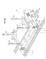
- a gate 160 which is formed in an 'n' shape is disposed so as to straddle a movement path of the stage 152. Respective end portions of the gate 160 are fixed at two side faces of the equipment pedestal 156. Sandwiching the gate 160, a scanner 162 is provided at one side, and a plurality (for example, two) of detection sensors 164 are provided at the other side. The detection sensors 164 detect a leading end and a trailing end of the optical wiring substrate 200. The scanner 162 and the detection sensors 164 are respectively mounted at the gate 160, and are fixedly disposed upward of the movement path of the stage 152. The scanner 162 and detection sensors 164 are connected to an unillustrated controller which controls the scanner 162 and detection sensors 164.
- the lens system 67 is structured with a single pair of combination lenses 71, which make the laser light that has been emitted from the fiber array light source 66 parallel, a single pair of combination lenses 73, which corrects the laser light that has been made parallel such that a light amount distribution is uniform, and a condensing lens 75 which focuses the laser light whose light amount distribution has been corrected on the DMD.
- the combination lenses 73 have the functions of, in the direction of arrangement of the laser emission ends, broadening portions of light flux that are close to an optical axis of the lenses and narrowing portions of the light flux that are distant from the optical axis, and in a direction intersecting this direction of arrangement, transmitting the light unaltered.
- the laser light is corrected such that the light amount distribution is uniform.
- the SRAM cell 60 which is fabricated with CMOS silicon gates by a continuous semiconductor memory production line, is disposed directly under the micromirror 62, with the support column, which includes a hinge and a yoke, interposed therebetween.
- the whole of this structure is monolithic (integrated).
- the micromirrors 62 supported at the support columns are inclined, about a diagonal, within a range of ⁇ o (for example, ⁇ 10o), relative to the side of the support at which the DMD 50 is disposed.
- Figure 7A shows a state in which the micromirror 62 is inclined at + ⁇ o, which is an 'ON' state
- Figure 7B shows a state in which the micromirror 62 is inclined at - ⁇ °, which is an 'OFF' state.
- a large number (for example, 800) of micromirrors are arranged in a long side direction to form a micromirror row, and a large number (for example, 600) of these micromirror rows are arranged in a short side direction.
- a pitch P 2 of scanning paths (scanning lines) of the exposure beams 53 from the micromirrors is tighter than a pitch P 1 of scanning lines in the case in which the DMD 50 is not inclined.
- a scanning width W 2 in the case in which the DMD 50 is inclined is substantially the same as a scanning width W 1 in the case in which the DMD 50 is not inclined.
- This multiple exposure functions for ovelappingly exposing two or more pixels includes: a function for superposing and exposing a plurality of pixels at the same position (superposedly exposing on the same scanning line); a function for superposing and exposing a plurality of pixels not at the same position but with centers thereof being mutually offset; and a function which combines the above functions.
- the micromirrors may be disposed in a staggered pattern in which the micromirror rows are shifted by predetermined intervals in the direction intersecting the sub-scanning direction, and the same effects can be obtained.
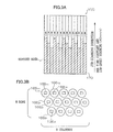
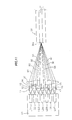
- the fiber array light source 66 is equipped with a plurality (for example, six) of laser modules 64. At each of the laser modules 64, one end of a multi-mode optical fiber 30 is connected. At the other end of the multi-mode optical fiber 30, an optical fiber 31, whose core diameter is the same as that of the multi-mode optical fiber 30 and whose cladding diameter is smaller than that of the multi-mode optical fiber 30, is connected. As shown in Figure 9C, emission end portions (light emission points) of the multi-mode optical fibers 31 are arranged in a single row along the main scanning direction, which intersects the sub-scanning direction, to structure a laser emission portion 68. Note that the light emission points may be arranged in two rows along the main scanning direction, as shown in Figure 9D.
- the emission end portions of the optical fibers 31 are inserted between a pair of support plates 65, which have flat faces, and fixed.
- a transparent protective plate 63 is disposed at the light emission side of the optical fibers 31 in order to protect end faces of the optical fibers 31.
- the protective plate 63 may be disposed to be closely contacted with the end faces of the optical fibers 31, or may be disposed such that the end faces of the optical fibers 31 are sealed.
- the emission end portions of the optical fibers 31 have high optical density, tend to attract dust, and are susceptible to deterioration. However, by disposing the protective plate 63, the adherence of dust to the end faces can be prevented and deterioration can be slowed.
- the emission ends of the optical fibers 31 with small cladding diameters are arranged in a single row without gaps therebetween, some of the multi-mode optical fibers 30, which are each between two of the multi-mode optical fibers 30 that are adjacent at the section with large cladding diameters, are piled up on the adjacent two of the multi-mode optical fibers 30.
- the emission end of the optical fiber 31 that is joined to the multi-mode optical fiber 30 that is piled up is arranged so as to be sandwiched between the two emission ends of the optical fibers 31 that are joined to the two multi-mode optical fibers 30 that are adjacent at the section with large cladding diameters.
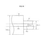
- optical fibers can be obtained by, for example, as shown in Figure 10, coaxially joining 1 to 30 cm lengths of the optical fibers 31 with small diameters to distal end portions, at the laser light emission side, of the multi-mode optical fibers 30 with large cladding diameters.
- the two types of optical fiber are joined by fusing incidence end faces of the optical fibers 31 to emission end faces of the multi-mode optical fibers 30 such that central axes of the pairs of fibers coincide.
- a diameter of a core 31a of the optical fiber 31 has the same magnitude as a diameter of a core 30a of the multi-mode optical fiber 30.
- a short-strip optical fiber at which the optical fiber whose cladding diameter is smaller is fused to an optical fiber whose length is short and whose cladding diameter is larger, may be joined at the emission end of the multi-mode optical fiber 30 via a ferrule, an optical connector or the like. Because the joining is carried out using the connector or the like so as to be detachable, replacement of a distal end portion, in a case in which the optical fiber whose cladding diameter is smaller has been damaged, is simple, and costs required for maintenance of the exposure head can be reduced.
- the optical fiber 31 may on occasions be referred to as an exposure end portion of the multi-mode optical fiber 30.
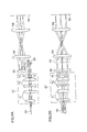
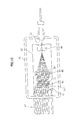
- the laser module 64 is structured by a multiplexed laser light source (fiber light source) shown in Figure 11.
- This multiplex laser light source is structured with a plurality (for example, seven) of chip-form lateral multi-mode or single-mode UV-type semiconductor lasers LD1, LD2, LD3, LD4, LD5, LD6 and LD7, collimator lenses 11, 12, 13, 14, 15, 16 and 17, a single condensing lens 20, and one of the multi-mode optical fibers 30.
- the UV-type semiconductor lasers LD1 to LD7 are fixedly arranged on a heat block 10.
- the collimator lenses 11 to 17 are provided in correspondence with the UV-type semiconductor lasers LD to LD7, respectively.
- the UV-type semiconductor lasers LD1 to LD7 all have the same oscillation wavelength and maximum output. Note that the number of semiconductor lasers is not limited to seven.
- the above-described multiplex laser light source is accommodated in a box-like package 40, which opens upward.
- the package 40 is provided with a package lid 41 prepared so as to close this opening of the package 40. After an air removal treatment, sealed gas is introduced and the opening of the package 40 is closed by the package lid 41.
- the above-described multiplex laser light source is hermetically sealed in a closed space (sealed space) formed by the package 40 and the package lid 41.
- a baseplate 42 is fixed at a lower face of the package 40.
- the heat block 10, a condensing lens holder 45 and a fiber holder 46 are attached at an upper face of the baseplate 42.
- the condensing lens holder 45 holds the condensing lens 20.
- the fiber holder 46 holds an incidence end portion of the multi-mode optical fiber 30.
- An opening is formed in a wall face of the package 40. The emission end portion of the multi-mode optical fiber 30 is passed through this opening and led out to outside the package.
- a collimator lens holder 44 is attached at a side face of the heat block 10, and holds the collimator lenses 11 to 17. Openings are formed in a lateral wall face of the package 40. Wiring 47, which supplies driving current to the UV-type semiconductor lasers LD1 to LD7, is passed through these openings and led out to outside the package.
- the laser beams B1 to B7 emitted from the light emission points are incident, respectively, on the collimator lenses 11 to 17 having the long, narrow forms described above, in states in which the direction for which the spreading angle of the beam is greater coincides with the length direction of the lens and the direction in which the spreading angle is smaller coincides with a width direction (a direction intersecting the length direction).
- the width of each of the collimator lenses 11 to 17 is 1.1 mm and the length thereof is 4.6 mm
- the laser beams B1 to B7 incident thereat have beam diameters in the horizontal direction and the vertical direction of 0.9 mm and 2.6 mm, respectively.
- the condensing lens 20 is cut away in a long, narrow shape with parallel flat faces defining a region that includes an optical axis of a circular-form lens which is provided with an aspherical surface, and is formed in a shape which is long in the direction of arrangement of the collimator lenses 11 to 17 (i.e., the horizontal direction) and short in a direction perpendicular thereto.
- the condensing lens 20 is formed by, for example, molding-formation of resin or optical glass.
- the respective laser beams B1, B2, B3, B4, B5, B6 and B7 which are emitted in divergent forms from the respective UV-type semiconductor lasers LD 1 to LD7 that structure the multiplex laser light source of the fiber array light source 66, are converted to parallel light by the corresponding collimator lenses 11 to 17.
- the laser beams B 1 to B7 that have been collimated are focused by the condensing lens 20, and converge at the incidence end face of the core 30a of the multi-mode optical fiber 30.
- a condensing optical system is structured by the collimator lenses 11 to 17 and the condensing lens 20, and a multiplexing optical system is structured by the condensing optical system and the multi-mode optical fiber 30.
- the laser beams B1 to B7 focused by the condensing lens 20 as described above enter the core 30a of the multi-mode optical fiber 30, are propagated in the optical fiber, multiplexed to a single laser beam B, coupled at the emission end portion of the multi-mode optical fiber 30, and emitted from the optical fiber 31.
- high-luminance light emission points as described above are arranged in a single row along the main scanning direction. Because a conventional fiber light source, in which laser light from a single semiconductor laser is focused at a single optical fiber, would have low output, a desired output could not be obtained without arranging these conventional light sources in a large number of rows. However, because the multiplex laser light source employed in the present embodiment has high output, a desired output can be obtained with only a small number of rows, for example, one row.
- Image data corresponding to an exposure pattern is inputted at the unillustrated controller connected to the DMD 50, and is temporarily stored in a frame memory in the controller.
- This image data is data which represents a density of each pixel structuring an image with a binary value (whether or not a dot is to be recorded).
- the substrate in fabrication of an optical wiring substrate provided with a plurality of levels of optical wiring circuitry, the substrate can be formed with greater ease by digital maskless exposure using light beams than by conventional mask exposure. Moreover, alignment, scaling and the like can be employed more easily, and consequently solid optical wiring circuitry can be positioned with higher accuracy.
- core layers and cladding layers which structure optical waveguides can be formed by maskless exposure, and fabrication of optical wiring circuitry and optical wiring substrates is simple.
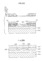
- this optical wiring substrate material is set on the stage 152 of the exposure apparatus 100 and a predetermined exposure pattern is exposed at the core layer 244 by laser light (UV light) irradiated from the scanner 162.
- a pattern formation (wiring) region of an optical wiring circuit to be structured by the core layer 244 is exposed by laser light.
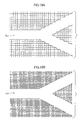
- the number of overlapping exposures by multiple exposure is reduced stepwise from an inner side to a distal end side, and a distribution of exposure light amounts (the arrows UV) controls exposure light amounts such that the predetermined region is inclined as shown in the drawing (at about 45o).
- a core layer, and inclined faces provided at end portions of the core layer can be formed by maskless exposure, and fabrication of optical wiring circuitry and optical wiring substrates is simple.
- the number of overlapping exposures by multiple exposure is reduced stepwise from an inner side to a distal end side of a predetermined region, which corresponds to an inclined face to be formed at the end portion of the core layer 244.
- the distributions of exposure light amounts (the arrows UVA and the arrows UVB) control exposure light amounts such that the predetermined region is inclined (at about 45o) as shown in the drawing. Consequently, an exposure region of the core layer 244 is exposed and cured.
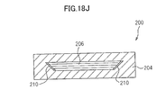
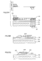
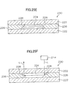
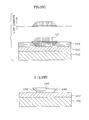
- FIG 29C metal is vapor-deposited at the inclined faces 246 at both end portions of the core layer 244A, and the thin film-form reflection mirrors 248 are formed.
- the core layer 244A is covered by the cladding layer 242 and, as shown in Figure 29D, a first level optical wiring circuit is formed, which is structured by an optical waveguide (the core layer 244A) at both end portions of which reflection mirrors are provided.
- the core layer 244 is formed on the cladding layer 242.
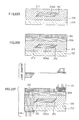
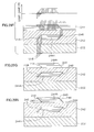
- exposure processing is again implemented by the exposure apparatus 171.
- a pattern formation region of the optical wiring circuitry and one end portion of the core layer 244 are exposed by laser light UVA from the scanner 162A disposed at the upper side.
- the number of overlapping exposures by multiple exposure is reduced stepwise from an inner side to a distal end side of a predetermined region which corresponds to an inclined face to be formed at the end portion of the core layer 244. Accordingly, the distribution of exposure light amounts (the arrows UVA) controls exposure light amounts such that the predetermined region is inclined (at about 45o) as shown in the drawing.
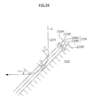
- the other end portion of the core layer 244 is exposed by laser light UVB from the scanner 162B disposed at the lower side.
- the laser light UVB irradiates a region corresponding to the reflection mirror 248 at the left side end portion of the first level core layer 244A.
- the distribution of exposure light amounts controls exposure light amounts so as to be inclined as shown in the drawing (at about 45o).
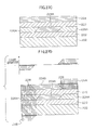
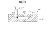
- FIG. 29G a trapezoid cross-section core layer 244B with an inverted taper face at the left side end portion thereof is formed.
- This core layer 244B has a parallelogram form which is vertically inverted relative to the first level core layer 244A. Positions of inclined faces of the two end portions of each core layer are disposed to respectively substantially overlap in the vertical direction.
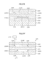
- the reflection mirrors 248 are formed at the inclined faces 246, at the two end portions of the core layer 244B, by vapor deposition of metal or the like.
- the core layer 244B is covered by the cladding layer 242 and the second level of optical wiring circuitry is formed.
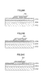
- the temporary support 202 is stripped away and, as shown in Figure 29J, an optical wiring substrate 260, in which optical wiring circuitry is provided at a plurality of levels, is completed.
- An example of usage of the optical wiring substrate 260 is shown in Figure 29J but, being similar to the case of the optical wiring substrate 220 shown in Figure 23, will not be described further.
- the substrate in the case of the method for fabrication of an optical wiring substrate provided with a plurality of levels of optical wiring circuitry by the direct exposure method, the substrate can be formed more easily by digital maskless exposure using a light beam than by conventional mask exposure. Moreover, similarly to the second and fourth embodiments, alignment, scaling and the like can be employed, and a plurality of levels of optical wiring circuitry can be positioned with high accuracy.
- MEMS microelectro-mechanical systems
- SLM spatial light modulators
- PZT elements optical elements
- FLC liquid crystal shutters
Applications Claiming Priority (2)
| Application Number | Priority Date | Filing Date | Title |
|---|---|---|---|
| JP2002167401 | 2002-06-07 | ||
| JP2002167401 | 2002-06-07 |
Publications (2)
| Publication Number | Publication Date |
|---|---|
| EP1372005A2 true EP1372005A2 (fr) | 2003-12-17 |
| EP1372005A3 EP1372005A3 (fr) | 2004-11-17 |
Family
ID=29561715
Family Applications (1)
| Application Number | Title | Priority Date | Filing Date |
|---|---|---|---|
| EP03012893A Withdrawn EP1372005A3 (fr) | 2002-06-07 | 2003-06-06 | Circuit optique intégré et procédé de sa réalisation |
Country Status (3)
| Country | Link |
|---|---|
| US (1) | US7197201B2 (fr) |
| EP (1) | EP1372005A3 (fr) |
| CN (1) | CN1467517A (fr) |
Cited By (2)
| Publication number | Priority date | Publication date | Assignee | Title |
|---|---|---|---|---|
| WO2006064363A1 (fr) * | 2004-12-14 | 2006-06-22 | Radove Gmbh | Processus et appareil de production de rayons uv de collimation pour transfert photolithographique |
| WO2015092016A1 (fr) * | 2013-12-20 | 2015-06-25 | Luxexcel Holding B.V. | Procédé pour imprimer une structure tridimensionnelle de guidage de la lumière par le durcissement de gouttelettes d'un matériau d'impression par irradiation de lumière |
Families Citing this family (19)
| Publication number | Priority date | Publication date | Assignee | Title |
|---|---|---|---|---|
| CN1308738C (zh) * | 2004-04-16 | 2007-04-04 | 南昌航空工业学院 | 高分辨力数字化微光学灰度掩模制作系统及制作方法 |
| WO2006009845A2 (fr) * | 2004-06-18 | 2006-01-26 | University Of Delaware | Procede et appareil pour sources optiques a base de modulateurs spatiaux de lumiere en mode reflexion pour communications globales entre puces |
| US7345806B2 (en) * | 2004-06-23 | 2008-03-18 | Texas Instruments Incorporated | Method and apparatus for characterizing microelectromechanical devices on wafers |
| BRPI0609507A2 (pt) * | 2005-04-02 | 2011-05-24 | Xeikon Ip Bv | dispositivo de exposição |
| JP2007003861A (ja) * | 2005-06-24 | 2007-01-11 | Fujifilm Holdings Corp | 露光方法および装置 |
| JP4277840B2 (ja) * | 2005-09-30 | 2009-06-10 | ミツミ電機株式会社 | 光導波路デバイスの製造方法 |
| TWI432908B (zh) * | 2006-03-10 | 2014-04-01 | Mapper Lithography Ip Bv | 微影系統及投射方法 |
| JP5498219B2 (ja) | 2009-03-26 | 2014-05-21 | パナソニック株式会社 | ミラー面を有する光導波路の製造方法及び光電複合配線板 |
| US8873912B2 (en) * | 2009-04-08 | 2014-10-28 | International Business Machines Corporation | Optical waveguide with embedded light-reflecting feature and method for fabricating the same |
| WO2012032465A2 (fr) * | 2010-09-10 | 2012-03-15 | Koninklijke Philips Electronics N.V. | Système de zoom optique à mélange amélioré comprenant une grille mobile et un gobo |
| US9103985B2 (en) | 2010-12-21 | 2015-08-11 | Nec Corporation | Optical waveguide device and a manufacturing method for an optical waveguide device |
| JP2013003224A (ja) * | 2011-06-14 | 2013-01-07 | Shinko Electric Ind Co Ltd | 光導波路及びその製造方法と光導波路装置 |
| JP6428146B2 (ja) * | 2014-10-22 | 2018-11-28 | 日本電気株式会社 | 光導波路デバイス及びその製造方法 |
| EP3224675A1 (fr) * | 2014-11-27 | 2017-10-04 | Carl Zeiss SMT GmbH | Appareil de lithographie comprenant une pluralité de têtes d'écriture pouvant être commandées individuellement |
| CN104977653B (zh) * | 2015-06-18 | 2018-03-23 | 湖南晶图科技有限公司 | 一种plc波导微耦合镜面的加工方法 |
| CN107688211B (zh) * | 2016-08-04 | 2020-09-25 | 苏州旭创科技有限公司 | 一种光波导器件及其制作方法 |
| WO2019010495A1 (fr) * | 2017-07-07 | 2019-01-10 | Arizona Board Of Regents On Behalf Of The University Of Arizona | Fabrication rapide de coupleur optique hors plan en polymère par lithographie à niveaux de gris |
| US10509164B2 (en) * | 2017-09-14 | 2019-12-17 | Lightwave Logic Inc. | Guide transition device and method |
| US10503071B2 (en) | 2017-10-26 | 2019-12-10 | Waymo Llc | Method for manufacturing light guide elements |
Citations (3)
| Publication number | Priority date | Publication date | Assignee | Title |
|---|---|---|---|---|
| US6312134B1 (en) * | 1996-07-25 | 2001-11-06 | Anvik Corporation | Seamless, maskless lithography system using spatial light modulator |
| WO2001090814A2 (fr) * | 2000-05-24 | 2001-11-29 | Ball Semiconductor, Inc. | Systeme d'exposition sans masque |
| WO2002041196A1 (fr) * | 2000-11-14 | 2002-05-23 | Ball Semiconductor, Inc. | Systeme de photolithographie numerique servant a fabriquer des elements diagonaux lisses |
Family Cites Families (14)
| Publication number | Priority date | Publication date | Assignee | Title |
|---|---|---|---|---|
| US5263111A (en) * | 1991-04-15 | 1993-11-16 | Raychem Corporation | Optical waveguide structures and formation methods |
| JP3079401B2 (ja) | 1993-03-17 | 2000-08-21 | 日本電信電話株式会社 | 光導波路端部ミラーの形成方法 |
| JP2616660B2 (ja) * | 1993-06-21 | 1997-06-04 | 日本電気株式会社 | 厚膜配線パターンの露光装置および厚膜の成形方法 |
| CA2130738A1 (fr) * | 1993-11-01 | 1995-05-02 | Keith Wayne Goossen | Methode et dispositif de fabrication de miroirs a inclinaison quelconque dans les substrats pour les systemes optiques hybrides |
| KR100288742B1 (ko) * | 1997-03-12 | 2001-05-02 | 윤종용 | 광도파로소자의제조방법 |
| US6356340B1 (en) * | 1998-11-20 | 2002-03-12 | Advanced Micro Devices, Inc. | Piezo programmable reticle for EUV lithography |
| US6516104B1 (en) * | 1999-06-25 | 2003-02-04 | Kabushiki Kaisha Toshiba | Optical wiring device |
| US6623665B1 (en) * | 2000-02-22 | 2003-09-23 | Lockheed Martin Corporation | Second-order nonlinear optics material, the devices using same and methods of preparing |
| US6509955B2 (en) * | 2000-05-25 | 2003-01-21 | Ball Semiconductor, Inc. | Lens system for maskless photolithography |
| JP2002082242A (ja) * | 2000-09-08 | 2002-03-22 | Toppan Printing Co Ltd | 光配線層及びその製造方法、並びに、光・電気配線基板及び実装基板 |
| JP2002351086A (ja) * | 2001-03-22 | 2002-12-04 | Fuji Photo Film Co Ltd | 露光装置 |
| JP4320694B2 (ja) * | 2001-08-08 | 2009-08-26 | 株式会社オーク製作所 | 多重露光描画装置および多重露光式描画方法 |
| JP2003340924A (ja) * | 2002-05-23 | 2003-12-02 | Fuji Photo Film Co Ltd | 積層造形装置 |
| JP2003340923A (ja) * | 2002-05-23 | 2003-12-02 | Fuji Photo Film Co Ltd | 光造形装置 |
-
2003
- 2003-06-06 CN CNA031411053A patent/CN1467517A/zh active Pending
- 2003-06-06 EP EP03012893A patent/EP1372005A3/fr not_active Withdrawn
- 2003-06-09 US US10/456,965 patent/US7197201B2/en not_active Expired - Lifetime
Patent Citations (3)
| Publication number | Priority date | Publication date | Assignee | Title |
|---|---|---|---|---|
| US6312134B1 (en) * | 1996-07-25 | 2001-11-06 | Anvik Corporation | Seamless, maskless lithography system using spatial light modulator |
| WO2001090814A2 (fr) * | 2000-05-24 | 2001-11-29 | Ball Semiconductor, Inc. | Systeme d'exposition sans masque |
| WO2002041196A1 (fr) * | 2000-11-14 | 2002-05-23 | Ball Semiconductor, Inc. | Systeme de photolithographie numerique servant a fabriquer des elements diagonaux lisses |
Cited By (3)
| Publication number | Priority date | Publication date | Assignee | Title |
|---|---|---|---|---|
| WO2006064363A1 (fr) * | 2004-12-14 | 2006-06-22 | Radove Gmbh | Processus et appareil de production de rayons uv de collimation pour transfert photolithographique |
| WO2015092016A1 (fr) * | 2013-12-20 | 2015-06-25 | Luxexcel Holding B.V. | Procédé pour imprimer une structure tridimensionnelle de guidage de la lumière par le durcissement de gouttelettes d'un matériau d'impression par irradiation de lumière |
| US10994474B2 (en) | 2013-12-20 | 2021-05-04 | Luxexcel Holding B.V. | Method for printing a three-dimensional light guiding structure by curing droplets of a printing material by light irradiation |
Also Published As
| Publication number | Publication date |
|---|---|
| US20040037487A1 (en) | 2004-02-26 |
| CN1467517A (zh) | 2004-01-14 |
| EP1372005A3 (fr) | 2004-11-17 |
| US7197201B2 (en) | 2007-03-27 |
Similar Documents
| Publication | Publication Date | Title |
|---|---|---|
| US7197201B2 (en) | Optical wiring substrate fabrication process and optical wiring substrate device | |
| US7121740B2 (en) | Laser apparatus, exposure head, exposure apparatus, and optical fiber connection method | |
| US7057706B2 (en) | Exposure device | |
| EP1426190B1 (fr) | Correction de l'inégalité causée par la déviation de l'angle d'inclinaison de la tête d'imagerie | |
| US7146081B2 (en) | Waveguide including a plurality of waveguide segments | |
| US6832045B2 (en) | Exposure device | |
| US7145639B2 (en) | Projecting exposure method | |
| EP1369731A2 (fr) | Tête d'exposition et dispositif d'exposition | |
| JP2004006440A (ja) | レーザ装置、露光ヘッド、及び露光装置 | |
| KR100796582B1 (ko) | 노광방법 및 장치 | |
| KR20100014785A (ko) | 노광 방법, 노광 장치 및 디바이스 제조 방법 | |
| JP6652618B2 (ja) | 照度割合変更方法及び露光方法 | |
| US20040184119A1 (en) | Imaging head unit, imaging device and imaging method | |
| JP2003345030A (ja) | 露光装置 | |
| US20050254032A1 (en) | Exposure device | |
| JP2004062157A (ja) | 光配線回路の製造方法、及びその光配線回路を備えた光配線基板 | |
| JP2005210112A (ja) | 露光方法および装置 | |
| US20040240813A1 (en) | Pattern writing apparatus | |
| KR100629209B1 (ko) | 레이저장치, 노광헤드, 노광장치 및 광섬유의 접속방법 | |
| JP4323335B2 (ja) | 画像露光方法および装置 | |
| US20060033906A1 (en) | Exposure device | |
| TWI274733B (en) | Forming method for tiny flow paths | |
| JP4014990B2 (ja) | 光ファイバの接続方法 | |
| JP2008076590A (ja) | 描画位置測定方法および装置 | |
| KR100542828B1 (ko) | 레이저 묘화 기법을 이용한 고분자 평면형 광도파로 제작장치 |
Legal Events
| Date | Code | Title | Description |
|---|---|---|---|
| PUAI | Public reference made under article 153(3) epc to a published international application that has entered the european phase |
Free format text: ORIGINAL CODE: 0009012 |
|
| AK | Designated contracting states |
Kind code of ref document: A2 Designated state(s): AT BE BG CH CY CZ DE DK EE ES FI FR GB GR HU IE IT LI LU MC NL PT RO SE SI SK TR |
|
| AX | Request for extension of the european patent |
Extension state: AL LT LV MK |
|
| PUAL | Search report despatched |
Free format text: ORIGINAL CODE: 0009013 |
|
| AK | Designated contracting states |
Kind code of ref document: A3 Designated state(s): AT BE BG CH CY CZ DE DK EE ES FI FR GB GR HU IE IT LI LU MC NL PT RO SE SI SK TR |
|
| AX | Request for extension of the european patent |
Extension state: AL LT LV MK |
|
| RIC1 | Information provided on ipc code assigned before grant |
Ipc: 7G 03F 7/20 B Ipc: 7G 02B 6/136 B Ipc: 7G 02B 6/122 A |
|
| 17P | Request for examination filed |
Effective date: 20050422 |
|
| 17Q | First examination report despatched |
Effective date: 20050518 |
|
| AKX | Designation fees paid |
Designated state(s): DE FR GB |
|
| 17Q | First examination report despatched |
Effective date: 20050518 |
|
| RAP1 | Party data changed (applicant data changed or rights of an application transferred) |
Owner name: FUJIFILM CORPORATION |
|
| STAA | Information on the status of an ep patent application or granted ep patent |
Free format text: STATUS: THE APPLICATION IS DEEMED TO BE WITHDRAWN |
|
| 18D | Application deemed to be withdrawn |
Effective date: 20080522 |