EP1369913A2 - Method of patterning inter-metal dielectric layers - Google Patents
Method of patterning inter-metal dielectric layers Download PDFInfo
- Publication number
- EP1369913A2 EP1369913A2 EP03253366A EP03253366A EP1369913A2 EP 1369913 A2 EP1369913 A2 EP 1369913A2 EP 03253366 A EP03253366 A EP 03253366A EP 03253366 A EP03253366 A EP 03253366A EP 1369913 A2 EP1369913 A2 EP 1369913A2
- Authority
- EP
- European Patent Office
- Prior art keywords
- layer
- via hole
- dielectric layer
- patterning
- dielectric
- Prior art date
- Legal status (The legal status is an assumption and is not a legal conclusion. Google has not performed a legal analysis and makes no representation as to the accuracy of the status listed.)
- Withdrawn
Links
Images



Classifications
-
- H—ELECTRICITY
- H10—SEMICONDUCTOR DEVICES; ELECTRIC SOLID-STATE DEVICES NOT OTHERWISE PROVIDED FOR
- H10P—GENERIC PROCESSES OR APPARATUS FOR THE MANUFACTURE OR TREATMENT OF DEVICES COVERED BY CLASS H10
- H10P14/00—Formation of materials, e.g. in the shape of layers or pillars
- H10P14/40—Formation of materials, e.g. in the shape of layers or pillars of conductive or resistive materials
-
- H—ELECTRICITY
- H10—SEMICONDUCTOR DEVICES; ELECTRIC SOLID-STATE DEVICES NOT OTHERWISE PROVIDED FOR
- H10W—GENERIC PACKAGES, INTERCONNECTIONS, CONNECTORS OR OTHER CONSTRUCTIONAL DETAILS OF DEVICES COVERED BY CLASS H10
- H10W20/00—Interconnections in chips, wafers or substrates
- H10W20/01—Manufacture or treatment
- H10W20/071—Manufacture or treatment of dielectric parts thereof
- H10W20/093—Manufacture or treatment of dielectric parts thereof by modifying materials of the dielectric parts
- H10W20/095—Manufacture or treatment of dielectric parts thereof by modifying materials of the dielectric parts by irradiating with electromagnetic or particle radiation
-
- H—ELECTRICITY
- H10—SEMICONDUCTOR DEVICES; ELECTRIC SOLID-STATE DEVICES NOT OTHERWISE PROVIDED FOR
- H10W—GENERIC PACKAGES, INTERCONNECTIONS, CONNECTORS OR OTHER CONSTRUCTIONAL DETAILS OF DEVICES COVERED BY CLASS H10
- H10W20/00—Interconnections in chips, wafers or substrates
- H10W20/01—Manufacture or treatment
- H10W20/071—Manufacture or treatment of dielectric parts thereof
- H10W20/081—Manufacture or treatment of dielectric parts thereof by forming openings in the dielectric parts
- H10W20/084—Manufacture or treatment of dielectric parts thereof by forming openings in the dielectric parts for dual-damascene structures
- H10W20/085—Manufacture or treatment of dielectric parts thereof by forming openings in the dielectric parts for dual-damascene structures involving intermediate temporary filling with material
-
- H—ELECTRICITY
- H10—SEMICONDUCTOR DEVICES; ELECTRIC SOLID-STATE DEVICES NOT OTHERWISE PROVIDED FOR
- H10W—GENERIC PACKAGES, INTERCONNECTIONS, CONNECTORS OR OTHER CONSTRUCTIONAL DETAILS OF DEVICES COVERED BY CLASS H10
- H10W20/00—Interconnections in chips, wafers or substrates
- H10W20/01—Manufacture or treatment
- H10W20/071—Manufacture or treatment of dielectric parts thereof
- H10W20/081—Manufacture or treatment of dielectric parts thereof by forming openings in the dielectric parts
Definitions
- the present invention relates to a method of patterning inter-metal dielectric layers and, more particularly, to a method of patterning inter-metal dielectric layers, wherein generation of a photoresist residue on a wall of a via hole is totally prevented by irradiating UV to the via hole after its formation.
- dual damascene process is on growing demand in the field of patterning metal circuit and, in FIG. 1, its conventional process is illustrated.
- dual dielectric layers that is upper and lower layers
- a via hole is formed through the lower dielectric layer to connect an upper and lower circuit to each other
- a metal is plugged in the pattern to form a resulting structure.
- the resulting structure obtained by the above process goes through CMP (Chemical and Mechanical Polishing) process and thereby a formation of the desired circuit on the semiconductor substrate is achieved.
- CMP Chemical and Mechanical Polishing
- the lower circuit 1 is formed on the semiconductor substrate, and a lower etch-stop layer 2, the lower dielectric layer 3, an upper etch-stop layer 4, and the upper dielectric layer 5 are sequentially layered on the substrate including the lower circuit 1.
- a photoresist is coated on the resulting substrate and, is exposed and developed to form a photoresist pattern 6.
- the developed substrate is firstly dry-etched using the photoresist pattern 6 as a mask to sequentially etch the upper dielectric layer 5, the upper etch-stop layer 4, and the lower dielectric layer 3, thereby forming a via hole 7 to expose the lower etch-stop layer 2 on the lower circuit 1.
- a photoresist 8 is then coated on the substrate including the via hole 7, and is exposed and developed to form a photoresist pattern 9.
- the upper dielectric layer 5 is secondly etched using the photoresist pattern 9 as the mask and, then, the upper and lower etch-stop layers 4 and 2 are simultaneously and secondly etched to form a via hole pattern to connect an upper metal circuit to both the upper and lower circuits.
- an amine group e.g. NH 2 -
- the amine group functions to trap H + ions in the photoresist during a photolithography process which is one of post-processes for forming the upper circuit line, and thus, after an exposure and development, a photoresist residue is not eliminated and left on the wall of the via hole. Accordingly, an undesirable pattern is formed during a second etching process, resulting in inferior electronic elements as shown in FIG. 2.
- a process of preventing trapping H + ions wherein a low-dielectric material (dielectric constant k ⁇ 3.2) containing fluorine is filled in a contact hole, and subjected to a photolithography process.
- This process is advantageous in that when a photoresist is stripped using an HF solution after an etching and ashing process of a low-dielectric layer, the low-dielectric material containing fluorine is stripped in conjunction with the photoresist. Accordingly, this process is useful in the case of using lower dielectric layers containing no pores and having a dielectric constant (k) of 2.7.
- the process is insufficiently competitive in the case of using the porous low-dielectric layers because it is difficult to secure a desired pattern when the etching rate of a nonporous low-dielectric material containing fluorine is not the same to that of the porous low-dielectric layer during etching the nonporous and porous dielectric layers.
- the nonporous low-dielectric material containing fluorine is slowly etched because the etching rate of the porous low-dielectric layer is higher than that of the low-dielectric layer containing no pores. Therefore, such a process fails to form proper damascene structure.
- a silanol group ( ⁇ Si-OH) is generated on the dielectric layers because the dielectric layers are exposed to plasma in the etching process of the dielectric layers, thereby making the wall of the via hole hydrophilic.
- ⁇ Si-OH silanol group
- an object of the present invention is to provide a method of patterning inter-metal dielectric layers by an dual damascene process, in which, after forming a via hole in a dielectric layers, UV rays are irradiated so as to modify a chemical structure of a wall of the via hole and to reduce its reactivity, thereby easily removing a photoresist residue, which is difficult to remove during a developing process.
- the above object can be accomplished by providing a method of patterning inter-metal dielectric layers, comprising steps of a) sequentially layering a lower etch-stop layer, a lower dielectric layer, an upper etch-stop layer, and an upper dielectric layer on a semiconductor substrate including a lower circuit patterned thereon, b) patterning the upper dielectric layer, the upper etch-stop layer, and the lower dielectric layer to form a via hole, exposing the lower etch-stop layer on the lower circuit, c) irradiating UV rays to the via hole, d) forming a photoresist layer on the resulting semiconductor substrate including the via hole thereon, and patterning the photoresist layer, e) patterning the upper dielectric layer using the patterned photoresist layer as an etching mask to form a circuit line around the via hole in the upper dielectric layer, and f) exposing an upper portion of the lower circuit.
- UV rays are irradiated to the via hole in order to modify a chemical structure of a wall of the via hole and to reduce its reactivity, thereby easily removing a photoresist residue, which is difficult to remove during developing a photoresist.
- a wall of the via hole of a low-dielectric layer containing nano-sized pores is subjected to a dehydroxylation to prevent the porous low-dielectric layer from absorbing water in a subsequent wet-cleaning process.
- FIG. 3 illustrates the chemical modification of the surface of the wall when UV rays being irradiated to the via hole in the dielectric layers, according to the present invention.
- most of amine groups on the surface of the via hole are bounded with hydrocarbon groups of a low-dielectric material and on the irradiation of the UV rays to the surface of the hole, a carbon-nitrogen bond is broken by the absorbed light energy.
- heat energy may be further added in conjunction with the UV rays so as to accelerate the bond-breakage.
- a silanol group is formed on the surface of the wall of the via hole in the case of using a porous material as the low-k (dielectric) layer as shown in FIG. 3.
- a porous material as the low-k (dielectric) layer as shown in FIG. 3.
- the UV rays are irradiated to the wall of the via hole, an O-H bond is broken, and the resulting oxygen radical attacks adjacent Si atoms to form a Si-O-Si bond.
- the wall surface of the via hole is made hydrophobic, thereby preventing an increase in a dielectric constant of the dielectric layers caused by the absorption of water into the dielectric layers and preventing a reduction in the performance of an electronic element which is mounted on the semiconductor substrate including the dielectric layers and the via hole.
- UV rays with a specific wavelength region may be irradiated to the low-dielectric layer using a laser beam as a light source, or UV rays with a relatively long wavelength of about 700 nm or lower may be irradiated to the low-dielectric layer using a UV lamp as the light source.
- various other light sources may be used to irradiate UV rays to the low-dielectric layer.
- UV rays with a wavelength of 150 to 400 nm can be used.
- heat energy of 100 to 300°C may be further supplied to the via hole in conjunction with the UV rays for a better results.
- the UV rays may be irradiated to the whole upper dielectric layer, or to a portion of the upper dielectric layer etched using the photomask and exposing devices, that is, to only the via hole.
- the present invention it is preferable to irradiate the UV rays to the via hole after forming the via hole but before coating a photoresist for a secondary exposing process on the dielectric layers.
- a SiO 2 layer, a SiOF layer, a SiOC layer, and a porous dielectric layer which are well known in the art, are useful as an inter-metal dielectric layer.
- the porous dielectric layer may be formed by various processes, for example, a chemical vapor deposition process, or a coating and hardening process of a precursor solution containing aerogel or xerogel materials, and surfactant or porogen materials, on the semiconductor substrate.
- Illustrative, but non-limiting examples of the surfactant include sulfates, sulfonates, phosphates, carboxylic acids, alkylammonium salts, gemini surfactants, cetylethylpiperidinium salts, dialkyldimethylammoniums, primary amines, poly(oxyethylene) oxides, octaethylene glycol monodecyl ether, octaethylene glycol monohexadecyl ether, and block copolymers thereof.
- porogen materials include polycaprolactones, cyclodextrins, poly(oxyethylene) oxides, octaethylene glycol monodecyl ether, octaethylene glycol monohexadecyl ether, and block copolymers thereof, but the porogen is not limited by the above examples.
- etch-stop layer useful in the present invention is a silicon carbide layer (SiC layer), a silicon carbonitride (SiCN) layer, a silicon nitride (SiN) layer, or amorphous silicon carbide (a-SiC) layer.
- SiC layer silicon carbide layer
- SiCN silicon carbonitride
- SiN silicon nitride
- a-SiC amorphous silicon carbide
- metal barrier and metal can be filled.
- materials for the metal barrier comprise at least one metal selected from the group consisted of Ti, TiN, Ta, TaN, and amorphous silicon carbide(SiC) and Examples of materials for the metal comprise copper.
- EXAMPLE 1 Comparison of chemical components constituting wall of a via hole before and after the irradiation of UV rays to the via hole
- dielectric layers SiOC layers without pores
- TOF-SIMS analysis Because of difficulty in analyzing the chemical components constituting the wall of the small-sized via hole, dielectric layers (SiOC layers without pores) were layered on a semiconductor substrate and dry-etched without a photoresist pattern under an N 2 gas atmosphere, and chemical components constituting surfaces of the SiOC layers were then analyzed instead of the chemical components of the via hole by TOF-SIMS analysis.
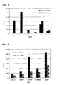
- FIG. 4 From FIG. 4, it can be seen that only hydrocarbons are detected after the layering process of the dielectric layers, but great quantities of hydrogen carbonitride and ammonia-based materials containing nitrogen are detected after the dry etch process of the dielectric layers.
- the dielectric layers SiOC layers without pores
- the dielectric layers were layered on the semiconductor substrate, dry-etched, and heated at 200°C while the UV rays were irradiated to the dielectric layers for 90 seconds, and the resulting structure was analyzed by TOF-SIMS analysis.
- a lower circuit was built on a semiconductor substrate, and a lower etch-stop layer, a lower dielectric layer, an upper etch-stop layer, and an upper dielectric layer were sequentially layered on the lower circuit.
- a silicon carbide (SiC) layer and a SiOC layer without pores were used as the upper and lower etch-stop layer and the upper and lower dielectric layer, respectively.
- a photoresist was then coated on the upper and lower dielectric layers, exposed and developed to form a photoresist pattern.
- the upper dielectric layer, upper etch-stop layer, and lower dielectric layer were sequentially dry-etched using the photoresist pattern as a mask to expose the lower etch-stop layer 2 positioned on the lower circuit, thereby forming the via hole in the dielectric layers.
- the via hole was irradiated by UV rays using a mercury light source for 60 seconds while being heated at 200°C to remove etched residue from the wall of the via hole and water absorbed/adsorbed into the wall of the via hole when the via hole is rinsed with water after the dielectric layers are etched.
- another via hole acting as a control sample was not subjected to the UV irradiation.
- the resulting semiconductor substrate irradiated by the UV rays was coated with the photoresist, exposed, and developed to form the photoresist pattern on the upper dielectric layer.
- the via hole subjected to the irradiation of the UV rays and the control sample were then photographed, and the results are shown in FIGs. 6 and 7. From FIGs. 6 and 7, it can be seen that the photoresist is not removed from the via hole of FIG. 7, while the via hole and photoresist pattern are desirably formed in the case of FIG. 6.
- the present invention is advantageous in that a metal circuit is formed in inter-metal dielectric layers according to the improved dual damascene process, thereby easily removing a photoresist residue, which is difficult to remove after developing the photoresist, and preventing an increase in the dielectric constant of a porous dielectric layer caused by the absorption of water into the porous dielectric layer.
- Another advantage of the present invention is that it is not necessary to conduct a dry procedure necessary in a wet etching process because the dielectric layers are etched according to a dry etching process, thus easily patterning inter-metal dielectric layers without additional drying devices.
Landscapes
- Internal Circuitry In Semiconductor Integrated Circuit Devices (AREA)
- Photosensitive Polymer And Photoresist Processing (AREA)
Abstract
Description
Claims (10)
- A method of patterning inter-metal dielectric layers, comprising:a) sequentially layering a lower etch-stop layer (2), a lower dielectric layer (3), an upper etch-stop layer (4), and an upper dielectric layer (5) on a semiconductor substrate, said semiconductor substrate including a lower circuit (1) patterned thereon;b) patterning the upper dielectric layer (5), the upper etch-stop layer (4), and the lower dielectric layer (3) to form a via hole (7), said via hole exposing the lower etch-stop layer (2) on the lower circuit (1);c) irradiating UV rays to the via hole (7);d) forming a photoresist layer (8) on the resulting semiconductor substrate including the via hole thereon, and patterning the photoresist layer (9);e) patterning the upper dielectric layer (5) using the patterned photoresist layer (9) as an etching mask to form a circuit line around the via hole (7) in the upper dielectric layer; andf) exposing an upper portion of the lower circuit.
- The method as claimed in claim 1, wherein each of the dielectric layers (3, 5) is selected from a SiO2 layer, a SiOF layer, a SiOC layer, and a porous dielectric layer.
- The method as claimed in claim 2, wherein the porous dielectric layer is formed by the steps of:1) coating a precursor solution on the semiconductor substrate to form a dielectric layer on the semiconductor substrate;2) baking the dielectric layer;3) curing the baked dielectric layer; and4) forming pores in the hardened dielectric layer using heat energy or UV rays.
- The method as claimed in claim 2, wherein the porous dielectric layer is formed by a chemical vapor deposition process.
- The method as claimed in claim 3, wherein the precursor solution contains aerogel or xerogel materials.
- The method as claimed in claim 3, wherein the precursor solution contains surfactant materials.
- The method as claimed in claim 3, wherein the precursor solution contains porogen materials.
- The method as claimed in any of claims 1 to 7, wherein the etch-stop layer (4) is a silicon carbide(SiC) layer, a silicon carbonitride(SiCN) layer, a silicon nitride (SiN) layer, or amorphous silicon carbide (a-SiC) layer.
- The method as claimed in any of claims 1 to 8, wherein the UV rays have a wavelength of 150 to 400 nm.
- The method as claimed in any of claims 1 to 9, wherein the UV rays are irradiated to the via hole (7) while heat energy at 100 to 300°C is supplied to the via hole.
Applications Claiming Priority (2)
| Application Number | Priority Date | Filing Date | Title |
|---|---|---|---|
| KR2002031547 | 2002-06-05 | ||
| KR1020020031547A KR20030093721A (en) | 2002-06-05 | 2002-06-05 | Method for Patterning Inter-Metal Dielectric Layer |
Publications (2)
| Publication Number | Publication Date |
|---|---|
| EP1369913A2 true EP1369913A2 (en) | 2003-12-10 |
| EP1369913A3 EP1369913A3 (en) | 2005-01-05 |
Family
ID=29546396
Family Applications (1)
| Application Number | Title | Priority Date | Filing Date |
|---|---|---|---|
| EP03253366A Withdrawn EP1369913A3 (en) | 2002-06-05 | 2003-05-29 | Method of patterning inter-metal dielectric layers |
Country Status (5)
| Country | Link |
|---|---|
| US (1) | US20040029386A1 (en) |
| EP (1) | EP1369913A3 (en) |
| JP (1) | JP2004096080A (en) |
| KR (1) | KR20030093721A (en) |
| CN (1) | CN1469452A (en) |
Cited By (1)
| Publication number | Priority date | Publication date | Assignee | Title |
|---|---|---|---|---|
| DE102008035815A1 (en) * | 2008-07-31 | 2010-02-04 | Advanced Micro Devices, Inc., Sunnyvale | Improve structural integrity and define critical dimensions of metallization systems of semiconductor devices using ALD techniques |
Families Citing this family (19)
| Publication number | Priority date | Publication date | Assignee | Title |
|---|---|---|---|---|
| JP5355892B2 (en) * | 2005-09-16 | 2013-11-27 | ルネサスエレクトロニクス株式会社 | Wiring structure, semiconductor device and manufacturing method thereof |
| US7514347B2 (en) * | 2005-10-13 | 2009-04-07 | United Microelectronics Corp. | Interconnect structure and fabricating method thereof |
| JP4567587B2 (en) * | 2005-12-12 | 2010-10-20 | 富士通株式会社 | Manufacturing method of semiconductor device |
| US7416990B2 (en) * | 2005-12-20 | 2008-08-26 | Dongbu Electronics Co., Ltd. | Method for patterning low dielectric layer of semiconductor device |
| JP5548332B2 (en) * | 2006-08-24 | 2014-07-16 | 富士通セミコンダクター株式会社 | Manufacturing method of semiconductor device |
| CN101140421B (en) * | 2006-09-04 | 2010-06-16 | 中芯国际集成电路制造(上海)有限公司 | Method for forming a photoresist pattern |
| JP2008103586A (en) * | 2006-10-20 | 2008-05-01 | Renesas Technology Corp | Semiconductor device manufacturing method and semiconductor device |
| JP4555320B2 (en) | 2007-06-15 | 2010-09-29 | 東京エレクトロン株式会社 | Low dielectric constant insulating film damage recovery method and semiconductor device manufacturing method |
| US20090042388A1 (en) * | 2007-08-10 | 2009-02-12 | Zhi-Qiang Sun | Method of cleaning a semiconductor substrate |
| CN100578731C (en) * | 2007-08-21 | 2010-01-06 | 联华电子股份有限公司 | Cleaning method of semiconductor substrate |
| KR101412144B1 (en) * | 2007-11-26 | 2014-06-26 | 삼성전자 주식회사 | METHOD FOR MANUFACTURING METAL WIRING AND METHOD FOR MANUFACTURING IMAGE SENSOR |
| KR20100006756A (en) * | 2008-07-10 | 2010-01-21 | 삼성전자주식회사 | Semiconductor device and method of fabricating the same |
| US9017933B2 (en) * | 2010-03-29 | 2015-04-28 | Tokyo Electron Limited | Method for integrating low-k dielectrics |
| CN102237296A (en) * | 2010-04-29 | 2011-11-09 | 中芯国际集成电路制造(上海)有限公司 | Through hole etching method |
| CN102877041B (en) * | 2011-07-14 | 2014-11-19 | 中国科学院微电子研究所 | Thin film deposition method and semiconductor device manufacturing method |
| US8871639B2 (en) | 2013-01-04 | 2014-10-28 | Taiwan Semiconductor Manufacturing Company, Ltd. | Semiconductor devices and methods of manufacture thereof |
| CN105702619A (en) * | 2014-11-27 | 2016-06-22 | 中芯国际集成电路制造(上海)有限公司 | Formation method of semiconductor structure |
| EP3332429B1 (en) * | 2015-08-03 | 2023-10-18 | Lumileds LLC | Semiconductor light emitting device with reflective side coating |
| CN108417532A (en) * | 2018-03-23 | 2018-08-17 | 上海华虹宏力半导体制造有限公司 | The forming method of contact plunger |
Family Cites Families (4)
| Publication number | Priority date | Publication date | Assignee | Title |
|---|---|---|---|---|
| JP3888794B2 (en) * | 1999-01-27 | 2007-03-07 | 松下電器産業株式会社 | Method for forming porous film, wiring structure and method for forming the same |
| US6420441B1 (en) * | 1999-10-01 | 2002-07-16 | Shipley Company, L.L.C. | Porous materials |
| EP1094506A3 (en) * | 1999-10-18 | 2004-03-03 | Applied Materials, Inc. | Capping layer for extreme low dielectric constant films |
| US6319809B1 (en) * | 2000-07-12 | 2001-11-20 | Taiwan Semiconductor Manfacturing Company | Method to reduce via poison in low-k Cu dual damascene by UV-treatment |
-
2002
- 2002-06-05 KR KR1020020031547A patent/KR20030093721A/en not_active Ceased
-
2003
- 2003-05-29 EP EP03253366A patent/EP1369913A3/en not_active Withdrawn
- 2003-06-03 CN CNA031386962A patent/CN1469452A/en active Pending
- 2003-06-04 JP JP2003159291A patent/JP2004096080A/en not_active Withdrawn
- 2003-06-05 US US10/454,488 patent/US20040029386A1/en not_active Abandoned
Cited By (2)
| Publication number | Priority date | Publication date | Assignee | Title |
|---|---|---|---|---|
| DE102008035815A1 (en) * | 2008-07-31 | 2010-02-04 | Advanced Micro Devices, Inc., Sunnyvale | Improve structural integrity and define critical dimensions of metallization systems of semiconductor devices using ALD techniques |
| US8105943B2 (en) | 2008-07-31 | 2012-01-31 | Globalfoundries Inc. | Enhancing structural integrity and defining critical dimensions of metallization systems of semiconductor devices by using ALD techniques |
Also Published As
| Publication number | Publication date |
|---|---|
| EP1369913A3 (en) | 2005-01-05 |
| KR20030093721A (en) | 2003-12-11 |
| CN1469452A (en) | 2004-01-21 |
| US20040029386A1 (en) | 2004-02-12 |
| JP2004096080A (en) | 2004-03-25 |
Similar Documents
| Publication | Publication Date | Title |
|---|---|---|
| EP1369913A2 (en) | Method of patterning inter-metal dielectric layers | |
| TWI488239B (en) | Method for removing insulating dielectric cover layer in interconnect structure | |
| US6319809B1 (en) | Method to reduce via poison in low-k Cu dual damascene by UV-treatment | |
| KR101283837B1 (en) | Method of treating dielectric film and method of forming feature | |
| US8183166B2 (en) | Dielectric layer structure and manufacturing method thereof | |
| US6444136B1 (en) | Fabrication of improved low-k dielectric structures | |
| JP5186086B2 (en) | Dual damascene patterning approach | |
| WO2008076663A1 (en) | Method for selective removal of damaged multi-stack bilayer films | |
| US6969683B2 (en) | Method of preventing resist poisoning in dual damascene structures | |
| US9236294B2 (en) | Method for forming semiconductor device structure | |
| US9004914B2 (en) | Method of and apparatus for active energy assist baking | |
| US6716741B2 (en) | Method of patterning dielectric layer with low dielectric constant | |
| JP2006073612A (en) | Resist removal method | |
| US6884728B2 (en) | Method for removing polymeric residue contamination on semiconductor feature sidewalls | |
| US7622403B2 (en) | Semiconductor processing system with ultra low-K dielectric | |
| CN100453487C (en) | Method for enhancing stability of fluorosilicone glass layer | |
| EP1764830B1 (en) | A method to create narrow trenches in dielectric materials | |
| CN1591820A (en) | Via First Dual Damascene Process | |
| JP2005072308A (en) | Method for removing resist and method for manufacturing semiconductor device | |
| Posseme et al. | In situ post etching treatment as a solution to improve defect density for porous low-k integration using metallic hard masks | |
| JP2006303422A (en) | Plasma processing method and semiconductor device manufacturing method | |
| JP2006041054A (en) | Ashing processing method and substrate processing method |
Legal Events
| Date | Code | Title | Description |
|---|---|---|---|
| PUAI | Public reference made under article 153(3) epc to a published international application that has entered the european phase |
Free format text: ORIGINAL CODE: 0009012 |
|
| AK | Designated contracting states |
Kind code of ref document: A2 Designated state(s): AT BE BG CH CY CZ DE DK EE ES FI FR GB GR HU IE IT LI LU MC NL PT RO SE SI SK TR |
|
| AX | Request for extension of the european patent |
Extension state: AL LT LV MK |
|
| PUAL | Search report despatched |
Free format text: ORIGINAL CODE: 0009013 |
|
| AK | Designated contracting states |
Kind code of ref document: A3 Designated state(s): AT BE BG CH CY CZ DE DK EE ES FI FR GB GR HU IE IT LI LU MC NL PT RO SE SI SK TR |
|
| AX | Request for extension of the european patent |
Extension state: AL LT LV MK |
|
| AKX | Designation fees paid | ||
| REG | Reference to a national code |
Ref country code: DE Ref legal event code: 8566 |
|
| STAA | Information on the status of an ep patent application or granted ep patent |
Free format text: STATUS: THE APPLICATION IS DEEMED TO BE WITHDRAWN |
|
| 18D | Application deemed to be withdrawn |
Effective date: 20050706 |