EP1367707A2 - System for controlling the delivery of power to dc computer components - Google Patents
System for controlling the delivery of power to dc computer components Download PDFInfo
- Publication number
- EP1367707A2 EP1367707A2 EP03016806A EP03016806A EP1367707A2 EP 1367707 A2 EP1367707 A2 EP 1367707A2 EP 03016806 A EP03016806 A EP 03016806A EP 03016806 A EP03016806 A EP 03016806A EP 1367707 A2 EP1367707 A2 EP 1367707A2
- Authority
- EP
- European Patent Office
- Prior art keywords
- regulation module
- voltage regulation
- voltage
- rectifier
- responsive
- Prior art date
- Legal status (The legal status is an assumption and is not a legal conclusion. Google has not performed a legal analysis and makes no representation as to the accuracy of the status listed.)
- Granted
Links
Images


Classifications
-
- H—ELECTRICITY
- H02—GENERATION; CONVERSION OR DISTRIBUTION OF ELECTRIC POWER
- H02M—APPARATUS FOR CONVERSION BETWEEN AC AND AC, BETWEEN AC AND DC, OR BETWEEN DC AND DC, AND FOR USE WITH MAINS OR SIMILAR POWER SUPPLY SYSTEMS; CONVERSION OF DC OR AC INPUT POWER INTO SURGE OUTPUT POWER; CONTROL OR REGULATION THEREOF
- H02M3/00—Conversion of dc power input into dc power output
- H02M3/22—Conversion of dc power input into dc power output with intermediate conversion into ac
- H02M3/24—Conversion of dc power input into dc power output with intermediate conversion into ac by static converters
- H02M3/28—Conversion of dc power input into dc power output with intermediate conversion into ac by static converters using discharge tubes with control electrode or semiconductor devices with control electrode to produce the intermediate ac
- H02M3/325—Conversion of dc power input into dc power output with intermediate conversion into ac by static converters using discharge tubes with control electrode or semiconductor devices with control electrode to produce the intermediate ac using devices of a triode or a transistor type requiring continuous application of a control signal
- H02M3/335—Conversion of dc power input into dc power output with intermediate conversion into ac by static converters using discharge tubes with control electrode or semiconductor devices with control electrode to produce the intermediate ac using devices of a triode or a transistor type requiring continuous application of a control signal using semiconductor devices only
- H02M3/33561—Conversion of dc power input into dc power output with intermediate conversion into ac by static converters using discharge tubes with control electrode or semiconductor devices with control electrode to produce the intermediate ac using devices of a triode or a transistor type requiring continuous application of a control signal using semiconductor devices only having more than one ouput with independent control
-
- E—FIXED CONSTRUCTIONS
- E02—HYDRAULIC ENGINEERING; FOUNDATIONS; SOIL SHIFTING
- E02D—FOUNDATIONS; EXCAVATIONS; EMBANKMENTS; UNDERGROUND OR UNDERWATER STRUCTURES
- E02D7/00—Methods or apparatus for placing sheet pile bulkheads, piles, mouldpipes, or other moulds
- E02D7/26—Placing by using several means simultaneously
-
- G—PHYSICS
- G06—COMPUTING; CALCULATING OR COUNTING
- G06F—ELECTRIC DIGITAL DATA PROCESSING
- G06F1/00—Details not covered by groups G06F3/00 - G06F13/00 and G06F21/00
- G06F1/26—Power supply means, e.g. regulation thereof
-
- H—ELECTRICITY
- H02—GENERATION; CONVERSION OR DISTRIBUTION OF ELECTRIC POWER
- H02J—CIRCUIT ARRANGEMENTS OR SYSTEMS FOR SUPPLYING OR DISTRIBUTING ELECTRIC POWER; SYSTEMS FOR STORING ELECTRIC ENERGY
- H02J1/00—Circuit arrangements for dc mains or dc distribution networks
- H02J1/002—Intermediate AC, e.g. DC supply with intermediated AC distribution
-
- H—ELECTRICITY
- H02—GENERATION; CONVERSION OR DISTRIBUTION OF ELECTRIC POWER
- H02J—CIRCUIT ARRANGEMENTS OR SYSTEMS FOR SUPPLYING OR DISTRIBUTING ELECTRIC POWER; SYSTEMS FOR STORING ELECTRIC ENERGY
- H02J1/00—Circuit arrangements for dc mains or dc distribution networks
- H02J1/08—Three-wire systems; Systems having more than three wires
- H02J1/082—Plural DC voltage, e.g. DC supply voltage with at least two different DC voltage levels
-
- H—ELECTRICITY
- H02—GENERATION; CONVERSION OR DISTRIBUTION OF ELECTRIC POWER
- H02M—APPARATUS FOR CONVERSION BETWEEN AC AND AC, BETWEEN AC AND DC, OR BETWEEN DC AND DC, AND FOR USE WITH MAINS OR SIMILAR POWER SUPPLY SYSTEMS; CONVERSION OF DC OR AC INPUT POWER INTO SURGE OUTPUT POWER; CONTROL OR REGULATION THEREOF
- H02M1/00—Details of apparatus for conversion
- H02M1/08—Circuits specially adapted for the generation of control voltages for semiconductor devices incorporated in static converters
- H02M1/088—Circuits specially adapted for the generation of control voltages for semiconductor devices incorporated in static converters for the simultaneous control of series or parallel connected semiconductor devices
-
- H—ELECTRICITY
- H02—GENERATION; CONVERSION OR DISTRIBUTION OF ELECTRIC POWER
- H02M—APPARATUS FOR CONVERSION BETWEEN AC AND AC, BETWEEN AC AND DC, OR BETWEEN DC AND DC, AND FOR USE WITH MAINS OR SIMILAR POWER SUPPLY SYSTEMS; CONVERSION OF DC OR AC INPUT POWER INTO SURGE OUTPUT POWER; CONTROL OR REGULATION THEREOF
- H02M3/00—Conversion of dc power input into dc power output
- H02M3/02—Conversion of dc power input into dc power output without intermediate conversion into ac
- H02M3/04—Conversion of dc power input into dc power output without intermediate conversion into ac by static converters
- H02M3/10—Conversion of dc power input into dc power output without intermediate conversion into ac by static converters using discharge tubes with control electrode or semiconductor devices with control electrode
- H02M3/145—Conversion of dc power input into dc power output without intermediate conversion into ac by static converters using discharge tubes with control electrode or semiconductor devices with control electrode using devices of a triode or transistor type requiring continuous application of a control signal
- H02M3/155—Conversion of dc power input into dc power output without intermediate conversion into ac by static converters using discharge tubes with control electrode or semiconductor devices with control electrode using devices of a triode or transistor type requiring continuous application of a control signal using semiconductor devices only
- H02M3/156—Conversion of dc power input into dc power output without intermediate conversion into ac by static converters using discharge tubes with control electrode or semiconductor devices with control electrode using devices of a triode or transistor type requiring continuous application of a control signal using semiconductor devices only with automatic control of output voltage or current, e.g. switching regulators
- H02M3/158—Conversion of dc power input into dc power output without intermediate conversion into ac by static converters using discharge tubes with control electrode or semiconductor devices with control electrode using devices of a triode or transistor type requiring continuous application of a control signal using semiconductor devices only with automatic control of output voltage or current, e.g. switching regulators including plural semiconductor devices as final control devices for a single load
-
- H—ELECTRICITY
- H02—GENERATION; CONVERSION OR DISTRIBUTION OF ELECTRIC POWER
- H02M—APPARATUS FOR CONVERSION BETWEEN AC AND AC, BETWEEN AC AND DC, OR BETWEEN DC AND DC, AND FOR USE WITH MAINS OR SIMILAR POWER SUPPLY SYSTEMS; CONVERSION OF DC OR AC INPUT POWER INTO SURGE OUTPUT POWER; CONTROL OR REGULATION THEREOF
- H02M3/00—Conversion of dc power input into dc power output
- H02M3/22—Conversion of dc power input into dc power output with intermediate conversion into ac
- H02M3/24—Conversion of dc power input into dc power output with intermediate conversion into ac by static converters
- H02M3/28—Conversion of dc power input into dc power output with intermediate conversion into ac by static converters using discharge tubes with control electrode or semiconductor devices with control electrode to produce the intermediate ac
- H02M3/325—Conversion of dc power input into dc power output with intermediate conversion into ac by static converters using discharge tubes with control electrode or semiconductor devices with control electrode to produce the intermediate ac using devices of a triode or a transistor type requiring continuous application of a control signal
- H02M3/335—Conversion of dc power input into dc power output with intermediate conversion into ac by static converters using discharge tubes with control electrode or semiconductor devices with control electrode to produce the intermediate ac using devices of a triode or a transistor type requiring continuous application of a control signal using semiconductor devices only
- H02M3/33507—Conversion of dc power input into dc power output with intermediate conversion into ac by static converters using discharge tubes with control electrode or semiconductor devices with control electrode to produce the intermediate ac using devices of a triode or a transistor type requiring continuous application of a control signal using semiconductor devices only with automatic control of the output voltage or current, e.g. flyback converters
- H02M3/33523—Conversion of dc power input into dc power output with intermediate conversion into ac by static converters using discharge tubes with control electrode or semiconductor devices with control electrode to produce the intermediate ac using devices of a triode or a transistor type requiring continuous application of a control signal using semiconductor devices only with automatic control of the output voltage or current, e.g. flyback converters with galvanic isolation between input and output of both the power stage and the feedback loop
-
- H—ELECTRICITY
- H02—GENERATION; CONVERSION OR DISTRIBUTION OF ELECTRIC POWER
- H02M—APPARATUS FOR CONVERSION BETWEEN AC AND AC, BETWEEN AC AND DC, OR BETWEEN DC AND DC, AND FOR USE WITH MAINS OR SIMILAR POWER SUPPLY SYSTEMS; CONVERSION OF DC OR AC INPUT POWER INTO SURGE OUTPUT POWER; CONTROL OR REGULATION THEREOF
- H02M3/00—Conversion of dc power input into dc power output
- H02M3/22—Conversion of dc power input into dc power output with intermediate conversion into ac
- H02M3/24—Conversion of dc power input into dc power output with intermediate conversion into ac by static converters
- H02M3/28—Conversion of dc power input into dc power output with intermediate conversion into ac by static converters using discharge tubes with control electrode or semiconductor devices with control electrode to produce the intermediate ac
- H02M3/325—Conversion of dc power input into dc power output with intermediate conversion into ac by static converters using discharge tubes with control electrode or semiconductor devices with control electrode to produce the intermediate ac using devices of a triode or a transistor type requiring continuous application of a control signal
- H02M3/335—Conversion of dc power input into dc power output with intermediate conversion into ac by static converters using discharge tubes with control electrode or semiconductor devices with control electrode to produce the intermediate ac using devices of a triode or a transistor type requiring continuous application of a control signal using semiconductor devices only
- H02M3/33569—Conversion of dc power input into dc power output with intermediate conversion into ac by static converters using discharge tubes with control electrode or semiconductor devices with control electrode to produce the intermediate ac using devices of a triode or a transistor type requiring continuous application of a control signal using semiconductor devices only having several active switching elements
- H02M3/33576—Conversion of dc power input into dc power output with intermediate conversion into ac by static converters using discharge tubes with control electrode or semiconductor devices with control electrode to produce the intermediate ac using devices of a triode or a transistor type requiring continuous application of a control signal using semiconductor devices only having several active switching elements having at least one active switching element at the secondary side of an isolation transformer
- H02M3/33592—Conversion of dc power input into dc power output with intermediate conversion into ac by static converters using discharge tubes with control electrode or semiconductor devices with control electrode to produce the intermediate ac using devices of a triode or a transistor type requiring continuous application of a control signal using semiconductor devices only having several active switching elements having at least one active switching element at the secondary side of an isolation transformer having a synchronous rectifier circuit or a synchronous freewheeling circuit at the secondary side of an isolation transformer
-
- E—FIXED CONSTRUCTIONS
- E02—HYDRAULIC ENGINEERING; FOUNDATIONS; SOIL SHIFTING
- E02D—FOUNDATIONS; EXCAVATIONS; EMBANKMENTS; UNDERGROUND OR UNDERWATER STRUCTURES
- E02D2250/00—Production methods
- E02D2250/0061—Production methods for working underwater
-
- H—ELECTRICITY
- H02—GENERATION; CONVERSION OR DISTRIBUTION OF ELECTRIC POWER
- H02M—APPARATUS FOR CONVERSION BETWEEN AC AND AC, BETWEEN AC AND DC, OR BETWEEN DC AND DC, AND FOR USE WITH MAINS OR SIMILAR POWER SUPPLY SYSTEMS; CONVERSION OF DC OR AC INPUT POWER INTO SURGE OUTPUT POWER; CONTROL OR REGULATION THEREOF
- H02M1/00—Details of apparatus for conversion
- H02M1/0083—Converters characterised by their input or output configuration
- H02M1/009—Converters characterised by their input or output configuration having two or more independently controlled outputs
-
- Y—GENERAL TAGGING OF NEW TECHNOLOGICAL DEVELOPMENTS; GENERAL TAGGING OF CROSS-SECTIONAL TECHNOLOGIES SPANNING OVER SEVERAL SECTIONS OF THE IPC; TECHNICAL SUBJECTS COVERED BY FORMER USPC CROSS-REFERENCE ART COLLECTIONS [XRACs] AND DIGESTS
- Y02—TECHNOLOGIES OR APPLICATIONS FOR MITIGATION OR ADAPTATION AGAINST CLIMATE CHANGE
- Y02B—CLIMATE CHANGE MITIGATION TECHNOLOGIES RELATED TO BUILDINGS, e.g. HOUSING, HOUSE APPLIANCES OR RELATED END-USER APPLICATIONS
- Y02B70/00—Technologies for an efficient end-user side electric power management and consumption
- Y02B70/10—Technologies improving the efficiency by using switched-mode power supplies [SMPS], i.e. efficient power electronics conversion e.g. power factor correction or reduction of losses in power supplies or efficient standby modes
Definitions
- Buck converter topologies are in current use for powering microprocessors. For a 2.5 volt, 13 ampere requirement, a switching frequency of 300 kHz is becoming inadequate. To meet substantial step load changes a large output capacitance is becoming required. As microprocessor voltage requirements move downward toward 1.0 volt at 50 amperes, the prior art topologies become even less suitable. With a drop in voltage (and an attendant drop in differential voltage tolerance) of 2.5 times, and an increase of current of 4 times, a larger output capacitor is now needed to maintain the required step response. It becomes increasingly difficult or impossible, however, to locate such a large capacitor close to the microprocessor connections. In addition, the cost of this approach increases with decreasing voltage. One solution to this problem has been to increase the frequency of the voltage regulation module.
- the non-resonant edges of this waveform cause problems such as the commutation of FET output capacitance and prevent increasing the switching frequency above about a megahertz.
- This situation is rapidly becoming serious as microprocessors and other low voltage electronics are ting developed which are increasingly difficult to provide suitable power for.
- the present invention permits the achievement of power for such needs. It permits higher frequencies and can be configured to handle higher currents.
- this invention specifically relates to powering computer systems.
- switch-mode DC is created to power the internal components of the system. It has particular applicability in new designs where microprocessors have high demands and power changes. Such can relate to the area of powering low voltage, high current electronics.
- the invention is applicable in the field of computing, and much of the following description is presented in that context. It should be understood, however, that other embodiments are in no way limited to the field of computing, and are applicable to a wide variety of circumstances wherein a variety of power absorbing loads which absorb electrical power may abruptly change their power absorbing characteristics (that is to say, their impedance may undergo a rapid change).
- microprocessor exhibit a lower maximum speed if operated at a lower voltage as compared to a higher operating voltage. That is, if a circuit is operating at full speed, and the voltage on that circuit is simply reduced, the circuit will not operate properly, and the speed of the circuit (the "clock speed") may have to be reduced. To maintain full speed capability and still operate at lower voltage, the circuit often must be redesigned to a smaller physical size. Also, as the size of the circuitry is reduced, and layer thickness is also reduced, the operating voltage may need to be lowered to maintain adequate margin to avoid breakdown of insulating oxide layers in the devices. For the past few years, these steps have defined the course of microprocessor design. Key microprocessor designers, seeking the maximum speed for their products, have therefore expended considerable effort trading off the following considerations:
- a processor may be drawing very little current because it is idling, and then an event may occur (such as the arrival of a piece of key data from a memory element or a signal from an outside event) which causes the processor to suddenly start rapid computation. This can produce an abrupt change in the current drawn by the processor, which has serious electrical consequences.
- Inductance is the measure of energy storage in magnetic fields. All current-carrying conductors have associated with their current a magnetic field, which represents energy storage. It is well known by workers in the art that the energy stored in a magnetic field is half the volume integral of the square of the magnetic field. Since the field is linearly related to the current in the conductor, it may be shown that the energy stored by a current carrying conductor is proportional to half the square of the current, and the constant of proportionality is called the "inductance" of the conductor.
- the energy stored in the system is supplied by the source of electrical current, and for a given power source there is a limit to the rate at which energy can be supplied, which means that the stored energy must be built up over time. Thus the presence of an energy storage mechanism naturally slows down a circuit, as the energy must be produced and metered into the magnetic field at some rate before the current can build up.
- V L * ⁇ I/ ⁇ t, where L is the inductance of the conductor, and ⁇ I / ⁇ t is the rate of change of current in the conductor.
- L the inductance of the conductor
- ⁇ I / ⁇ t the rate of change of current in the conductor.
- microprocessors operate at about two volts, and can tolerate a voltage transient on their supply lines of about 7%, or 140 millivolts. These same microprocessors can require that their supply current change at a rate of at least one-third or even nearly one ampere per nanosecond, or 3*10 8 or 10 9 amperes/second, respectively.
- Switchmode power conversion systems are powered by switchmode power conversion systems. Such a system converts incoming power from the utility line to the voltages and currents required by the electronic circuitry by operation of one or more switches. In low power business and consumer electronics, such as desktop personal computers, the incoming power is supplied as an alternating voltage, generally 115 volts in the United States, and 220 volts in much of the rest of the world. The frequency of alternation is either 50 or 60 Hertz, depending upon location. Such utility power must be converted to low voltage steady (direct) current, or dc, and regulated to a few percent in order to be useful as power for the electronic circuits. The device which performs such conversion is called a "power supply".
- switchmode conversion systems are powered by switchmode conversion systems. These systems typically operate as follows.
- the incoming utility power is first converted to unregulated direct current by a rectifier.
- the rectified DC is then converted to a higher frequency, typically hundreds of kilohertz, by electronic switches.
- This higher frequency power is then transformed by a suitable transformer to the appropriate voltage level; this transformer also provides isolation from the utility power, required for safety reasons.
- the resulting isolated higher frequency power is then rectified again, and filtered into steady direct current for use by the electronics. Regulation of the output voltage is usually accomplished by control of the conduction period of the electronic switches.
- the 5 resulting power conversion unit is smaller and lighter in weight than earlier approaches because the size and weight of the transformer and output filter are reduced proportionally to the increase in frequency over the basic utility power frequency. All of this is well known in the prior art.
- various voltages may be required.
- the peripherals such as disk drives
- the peripherals may require +12 volts
- some logic circuits may require +5 volts
- input/output circuits may additionally require -12 volts
- memory interface and general logic may require 3.3 volts
- the central microprocessor may require 2 volts.
- Standards have developed so that the central power source (the device that is connected directly to the utility power) delivers ⁇ 12 and +5 volts, and the lower voltages are derived from the +5 supply line by additional circuitry, called voltage regulation modules, or VRMs, near to the circuits that require the lower voltage.
- VRMs voltage regulation modules
- a typical 50 watt voltage regulation module which may convert +5 volts at 10 amperes to +2 volts at 25 amperes for the microprocessor, will itself have losses of about one watt each in the AC conversion and transformer, and ten watts in the final rectification and filtering.
- Other voltage regulation modules will have losses almost as great, resulting in losses for the entire system which may be one-third of the power used.
- Some particularly inefficient approaches may demonstrate efficiencies as low as 50%, requiring that the input power circuits utilize twice the power required by the actual final circuitry, and requiring that twice the heat be dissipated in the electronics (which must be removed by a fan) as is theoretically required by the actual operating circuitry.
- a further problem in the prior art is the use of square wave electronic conversion techniques.
- Such technology known as PWM, for Pulse Width Modulation, produces switch voltage waveforms which have steeply rising edges. These edges produce high frequency power components which can be conducted or radiated to adjacent circuitry, interfering with their proper operation. These high frequency power components may also be conducted or radiated to other electronic equipment such as radio or television receivers, also interfering with their proper operation.
- the presence of such components requires careful design of the packaging of the power system to shield other circuitry from the high frequency power components, and the installation of expensive and complex filters to prevent conduction of these components out of the power supply package on its input and output leads. What is needed then, is a power conversion system which enables small, highly efficient voltage regulation modules to be placed close to the point of power use, which is fast overall, and which is itself efficient and at least as low in cost as the prior art technology it replaces.
- a further object of the present invention is to provide a source of high frequency power which is substantially smaller than that of the prior art. Similarly it is an object to provide a source of low voltage at high current which is substantially smaller than that of the prior art to permit such a source to be placed in very close proximity to the electronic load.
- Another fundamental aspect of the invention is the potential for the affirmative use of the transformer leakage inductance. This can be necessary as the DC output voltage requirement is lowered.
- Another benefit of this invention involves the very nature of a power source. By incorporating some or all these elements it can be possible to provide power remotely. By making the output capacitance consist of only the bypass capacitors necessary on the microprocessor pins, the circuit feeding the microprocessor assembly can have essentially an inductive output.
- yet other objects include providing a circuit and method for providing power to electronics with low voltage, high current and high di/dt requirements, providing substantially higher power conversion frequencies, providing a circuit which allows a reasonable amount of transformer leakage inductance and switching device capacitances, providing a circuit or method whereby the synchronous rectifiers (SR's) always switch with zero voltage across the device, allowing high frequency operation, providing a circuit or method whereby the control signal to the SR operates in a non-dissipative fashion, allowing HF operation, and providing a reduced size of the output capacitance through HF operation.
- SR's synchronous rectifiers
- the present invention is directed to a system of energy storage which can store more energy and be placed physically farther from the powered electronics, through the reduction of magnetic fields surrounding the electrical connections and the magnetic energy stored therein, thereby creating a faster responding circuitry, and simplifies the design and reduces the cost of the line filters used to avoid conducted interference along the utility power lines. Also, distribution of low DCvoltages (e.g., 5 volts) results in relatively higher losses in the distribution wires and connectors when compared to the use of medium voltage alternating distribution levels (e.g., 30 volts rms), which nevertheless remain safe to touch.
- medium voltage alternating distribution levels e.g. 30 volts rms
- a DCpowered computer system comprising:
- Said computer component responsive to said remote power DCsupply system may comprise a component operating at a nominal DCvoltage selected from a group consisting of less than about 2 volts, less than about 1.8 volts, less than about 1.5 volts, less than about 1.3 volts, less than about 1 volt, and less than about 0.4 volts.
- Said computer component may be capable of a rapid current demand which rises at a level selected from a group consisting of at least about 0.2 amperes per nanosecond, at least about 0.5 amperes per nanosecond, at least about 1 ampere per nanosecond, at least about 3 amperes per nanosecond, at least about 10 amperes per nanosecond, and at least about 30 amperes per nanosecond.
- Said computer component may comprise a component operating at a maximum current selected from a group consisting of more than about 15 amperes, more than about 20 amperes, more than about 50 amperes, and more than about 100 amperes.
- Said passive rectifier control to which said first and said second switched voltage regulation module rectifier elements are responsive may comprise an alternating control input.
- Said alternating control input may comprise a sinusoidal drive system to which said first switched voltage regulation module rectifier element and said second switched voltage regulation module rectifier element are responsive.
- Said voltage regulation module may further comprise:
- Said voltage regulation module may further comprise an alternating input voltage regulator to which said voltage regulation module transformer is responsive.
- Said alternating input voltage regulator may comprise a variable capacitor.
- Said alternating input voltage regulator may comprise a series switch element.
- Said series switch element may comprise two switch elements.
- Said alternating input voltage regulator may comprise a regulator isolation element
- Said two switch elements may comprise switch elements driven at about a 180 degree phase relationship.
- Said voltage regulation module may further comprise a DCoutput coupling responsive to both said first rectifier inductive output and said second rectifier inductive output
- Said voltage regulation module may further comprise a third harmonics trap.
- Said voltage regulation module transformer may have a primary side and wherein said third harmonics trap comprises a third harmonics trap electrically tied to said primary side of said voltage regulation module transformer element
- Said step of transmitting said component DC supply voltage to an electrically remote computer component may comprise the step of transmitting said component DC supply voltage to over a distance selected from a group consisting of over at least about one-half inch, over at least about one inch, and over at least about two inches.
- Said step of transmitting said component DC supply voltage may comprise the step of transmitting said component DC supply voltage at a nominal DC voltage selected from a group consisting of less than about 2 volts, less than about 1.8 volts, less than about 1.5 volts, less than about 1.3 volts, less than about 1 volt, and less than about 0.4 volts.
- Said step of transmitting a component DC supply voltage may comprise the step of transmitting a component DC supply voltage through a DC output system capable of a rapid current demand which rises at a level selected from a group consisting of at least about 0.2 amperes per nanosecond, at least about 0.5 amperes per nanosecond, at least about 1 ampere per nanosecond, at least about 3 amperes per nanosecond, at least about 10 amperes per nanosecond, and at least about 30 amperes per nanosecond.
- Said step of transmitting a component DC supply voltage may comprise the step of transmitting a component DC supply voltage through a DC output system operating at a maximum current selected from a group consisting of more than about 15 amperes, more than about 20 amperes, more than about 50 amperes, and more than about 100 amperes.
- Said step of transmitting said component DC supply voltage to an electrically remote computer component may comprise the step of transmitting said component DC supply voltage through a substantially non-capacitive DC output system.
- Said step of transmitting said component DC supply voltage through a substantially non-capacitive DC output system may comprise the step of transmitting said component DC supply voltage through a substantially non-capacitive DC output system having an effective capacitance selected from a group consisting of less than about 0.3 millifarads, less than about 0.5 millifarads, less than about 1 millifarads, less than about 3 millifarads, less than about 10 millifarads, about only the inherent capacitance of a response network, about only an inherent reactance of a component connector, about only an inherent capacitance of said computer component, about only a bypass capacitance of a microprocessor, and any permutations or combinations of the above.
- the method may further comprise the step of electrically isolating said alternating power output prior to accomplish said step of establishing a component DC supply voltage.
- Said step of electrically isolating said alternating power output may comprise the step of transforming said alternating power output at said electrically remote location.
- Said step of rectifying said AC utility power to a DC signal may comprise the step of driving at least one rectifier element using a drive input and further comprising the step of electrically isolating said drive input at said electrically remote location.
- Said step of distributing power to an electrically remote location may comprise the step of utilizing substantially sinusoidal alternating signal power.
- Said step of utilizing substantially sinusoidal alternating signal power may comprise the step of utilizing substantially sinusoidal alternating signal power operating at a frequency selected from a group consisting of a frequency greater than at least about 300 kHz, a frequency greater than at least about 500 kHz, a frequency greater than at least about 1 MHz, a frequency greater than at least about 3 MHz, a frequency greater than at least about 10 MHz, a frequency greater than at least about 30 MHz, a frequency coordinated with an inherent capacitance of a first and a second switched voltage regulation module rectifier, a frequency coordinated with an inherent capacitance of said computer component, a frequency coordinated with an inherent capacitance of a component connector, a frequency coordinated with an inherent capacitance of a sinusoidal drive system, and any permutations or combinations of the above.
- Figure 3-5 shows one gate drive embodiment for the SR's according to the present invention.
- Figure 3-6 shows a circuit for voltage control on the primary side with a single switching design.
- Figure 3-7 shows a family of drain to source voltages as a function of the control input voltage across the FET.
- Figure 3-8 shows a circuit for voltage control on the primary side with a dual switching design.
- FIG. 3-9 a, b, c & d shows various synchronous rectification circuits according to the invention.
- Figure 3-10 shows a bulk capacitor and a by pass capacitor arrangement as applied to a microprocessor system in the prior art.
- Figure 3-11 shows an overall preferred embodiment of the invention using a single switch control element.
- Figure 3-12 shows an overall preferred embodiment of the invention using a dual switch control element.
- Figure 3-13 shows an overall preferred embodiment of important aspects of the aspect of the design.
- Figure 3-14 shows yet another preferred embodiment of a voltage regulation module design using a variable capacitor for primary side regulation.
- Figure 3-15 is a Smith chart showing a range of VRM input impedances vs load current percentage for one design of the present invention.
- the central power supply provides several standard voltages for use by the electronics.
- utility power typically at 110 or 220 volt nominal AC power alternating at 50 or 60 cycles, is converted by power supply (106) to standard DCvoltages, usually ⁇ 12 and +5 volts. These voltages are brought out of the power supply on flying leads, which form a kind of distribution system (107), terminated in one or more connectors (108)
- These standard voltages are useful directly for powering most of the input/output circuitry (140) and peripherals (144), such as a hard disc, floppy disc, and compact disc drives.
- CPU central processing unit
- DRAM dynamic random access memory
- VRM Voltage Regulation Module
- utility power (101) enters the silver box and is converted to unregulated DCpower by rectifier unit, or AC/DC converter (102).
- the resulting DCpower 5 is then re-converted to alternating current power at a higher frequency by inverter unit (103) (also called a DC/AC converter).
- inverter unit (103) also called a DC/AC converter.
- the higher frequency AC is galvanically connected to and is at the voltage level of utility power (101).
- Safety considerations require isolation from utility power (101), and as the required output voltage is much lower than that of utility power (101), voltage reduction is also needed. Both of these functions are accomplished by transformer (104).
- the resulting isolated, low voltage AC is then rectified to direct or multiply direct current power output(s) by rectifier and filter unit (105), distributed to the circuitry loads by distribution wiring (107) and connectors (108).
- specific standard voltages ⁇ 12 and +5 volts must be converted to lower voltages for CPU (141), memory (143) and management logic (145), by VRM unit (112).
- the standard DCvoltage from power supply unit (106) (usually +5 volts) is converted to alternating power again by DC/AC converter (109), transformed to the lower voltage by transformer (110), and re-rectified to the proper low voltage by AC/DC unit (111).
- VRM (112) the source of power, which for CPU unit (141) (and other low voltage circuits) is VRM (112), to be close to the circuit load. While for the near term designs the rate of change of current can be handled by capacitive energy storage, for future designs at still lower voltages and higher currents VRM unit (112) must be made extraordinarily small so that it can be placed close to its circuit load, and also must operate at a very high frequency so that large amounts of energy storage are not required. The requirement for low energy storage is rooted in the two facts that there is no physical room for the larger storage elements and no tolerance for their higher intrinsic inductance. Thus a requirement emerges that the frequency of VRM (112) must be increased.
- transformers (104) and (110) Another redundancy exists in principle, between transformers (104) and (110), but the desire to provide isolated power in the distribution system (107) mandates the use of transformer (104), and the requirement for different voltages for the different loads may also require the various VRMs to utilize transformer (110). Assuming that these elements are left in place, then, the use of high frequency AC distribution produces a system as shown in Figure 1-4. Thus one embodiment is directed specifically to the simplified VRM. Such an arrangement also permits electrically remote location of power element (e.g. at locations where the lead inductance would have otherwise have come into play using the prior techniques).
- central power supply (147) converts utility power (101) to DCpower by AC/DC converter (146). This DCpower is then converted to high frequency sinusoidal power by DC/AC converter (113).
- the sinusoidal power (or perhaps “substantially” or “approximately” sinusoidal power, as may be produced by even a less than ideal inverter or the like) is distributed to the location of use of the power, where high frequency VRMs (118) convert the sinusoidal power to low voltage, high current power for the circuit loads such as CPU (141), input/output circuits (140), logic management circuits (145), and memory (143).
- a VRM is required not only for the aforementioned low voltage circuits, but also for peripherals (144), since the DC power (likely +12 volt) requirement for these units is not supplied by the central power supply (106).
- the central power supply (106) may supply only sinusoidal high frequency AC power in this approach).
- High Frequency Transformer (114) may thus provide galvanic isolation and may transform the voltage from constant voltage Sinusoidal DC/AC Converter (113) to a level considered safe to touch.
- the present invention may be modified to provide a constant current as well. That is, as those of ordinary skill in the art would readily understand, it is possible to modify the described circuit so that a constant current is delivered into a load which varies from nominal to a short circuit, for use in constant current applications.
- Converter (113) may be designed to provide a constant output voltage with low THD, independent of load
- Some of the embodiments presented herein depend upon being supplied with a constant input DCvoltage from converter (146). It would of course also be possible to create this constant distribution voltage by feedback internal to converter (113), as an alternative, which then would not require a constant input voltage from converter (146).
- the latter approach - creating constant voltage through feedback - requires that the feedback system have very high bandwidth (high speed) in order to maintain the output voltage very close to constant against any output load variation, even on a nanosecond time scale. This feedback approach may be difficult and expensive to achieve, and the present invention is directed to accomplishing a constant voltage from converter (113) by the intrinsic operation of the circuit, without feedback.
- Figure 1-5 shows one embodiment of a constant voltage high frequency power source to accomplish the function of converter (113).
- DCpower source (119) is the circuit representation of the constant voltage from converter (146), and load (128) represents the constellation of loads connected to distribution system (115) (including the effects of connectors (18) and distribution system) (115).
- the voltage from source (119) is converted to a constant current by inductor (120) and either shunted by switch (122) when the switch is ON, or permitted to flow into network (148), comprising the elements in parallel with switch (122) when the switch is OFF.
- the network thus acts as a response network, that is, one which acts after the switch has transitioned.
- the voltage across switch (122) is approximately zero when switch (122) is ON and is dependent upon the response of network (148) when switch (122) is OFF.
- This response waveform, or "switch voltage waveform” is transformed by network (48) to form the voltage across load (128).
- the values of elements (123), (124), (125), and (126) may be chosen to cause the waveform across switch (122) to be approximately zero, or to be a desired fixed value, at the moment when switch (122) begins to conduct. Clear descriptions for the methodology for accomplishing this may be found in U.S. patents 3,919,656 and 5,187,580.
- the conductance of load (128) may be changed to the maximum nominal value, and the value of inductor (127) chosen to return the value of voltage across switch (122 )at the commencement of its ON period to the value chosen in the first step.
- This algorithm will result in a circuit for which the value of the switch voltage waveform at the commencement of the ON period of switch (122) is nearly independent of the value of the conductance of load (128), within the defined nominal range. It also results in a circuit for which the shape of the switch voltage waveform varies minimally over the range of the conductance of load (128).
- a significant function ofthe network formed by elements (123), (124), (125), (126), and (127) is to form a sinusoidal waveform across load (128).
- this is a linear passive network, namely, a network with no active elements (including but not limited to steering diodes, diodes generally, other active elements, or the like) or a network without some type of feedback element (an element which senses a condition and then responds to that condition as a result of a delayed decision-type of result), if the shape of the switch voltage waveform does not change in any substantial way, and especially if the fundamental frequency component of the switch-voltage waveform (the Fourier component of the waveform at the operating frequency) does not change substantially, for this circuit the value of the sinusoidal voltage across load (128) will not change substantially.
- the fundamental frequency component of the switch-voltage waveform the Fourier component of the waveform at the operating frequency
- a unique element of the invention is its high efficiency over the entire load range from a nominal load to an open circuit or from a nominal load to a short circuit. (As one skilled in the art should understand, one way to achieve one as opposed to the other simply involves altering the AC distribution system by one-quarter wavelength.) This comes about largely as 5 a result of the constant switch waveform described above. Since the voltage waveform changes but little over the load range, switching losses in the circuit are not affected by load variations. It should also be noted that all of the benefits of this invention are obtained without changing the frequency of operation. Thus, high efficiencies such as at least about 80%, at least about 85%, at least about 90%, at least about 95%, at least about 98% and even at least about 99% efficiency and beyond can be attained.
- Such a circuit which provides a constant voltage sinusoidal output across a load (or even in not strictly "across” the load, more generically “to which the load is responsive” thus encompassing bit direct and indirect responsiveness) which can vary at high speed, utilizing a single or multiple switch and a simple circuit, operating at constant frequency, while maintaining high efficiency over the entire load range, is a unique aspect of this invention in the field of power conversion.
- Another unique element of the invention is in the nature of the method of driving switch (122). As has been pointed out previously, efficiency is important in these applications, and it is desirable not to waste energy anywhere, including the circuit used to drive switch (122). It is in the nature of high frequency switches such as Field Effect Transistors (FETs) that they have a large input capacitance. Circuits which change the voltage on the gate terminal in a square-wave manner must first charge that capacitance to a voltage well above the gate threshold voltage for switch (122), turning ON the FET, and in the process deposit energy into that capacitance. It must then discharge that capacitance to a voltage well below the gate threshold voltage for switch (122), in the process absorbing the energy stored in the gate capacitance.
- FETs Field Effect Transistors
- the power lost in the process is the energy stored in the gate capacitance, multiplied by the frequency of operation, and this can be a substantial number. In the present invention this loss is avoided by affirmatively utilizing the gate capacitance of switch (122), thus coordinating the circuitry to the gate or capacitance. That is, the energy stored in the gate capacitance during the period switch (122) is ON is, in the present invention, stored in another element of the system during the period switch (122) is OFF, and is thereby available on the next cycle to return the gate above the threshold voltage for the next ON period. This may be accomplished by "resonating" the gate capacitance (or the effective capacitance of the system) with a series or parallel inductor.
- FET switch (122) is depicted as an internal switch device (139) with an explicit gate capacitance (138), shown separately.
- Gate drive circuit (121) contains inductor (136) connected in series (or in parallel as shown in the dotted-line alternate connection) (137) which is selected such that the reactance of inductor (136) or (137) is equal to the reactance of capacitor (138) at the 0 frequency of operation. In this way the energy in the gate system is transferred from gate capacitor (138) to inductor (136) (or its alternate) (137) and back again each cycle, and only the inevitable losses in the inductor and gate resistance need to be regenerated for each cycle.
- the gate voltage is substantially sinusoidal.
- the duty cycle of the system (that is, the fraction of the total period that switch (122) is ON) is determined by the fraction of the sinusoidal cycle which is substantially above the threshold voltage of switch (122).
- the duty cycle of switch (122) may be controlled by the magnitude of the sinusoidal signal, such an approach places limits on the available range of duty cycle, and also may result in longer than desirable commutation times (that is, the fraction of the total period during which the switch is transitioning from the ON to the OFF state), which may increase the losses of switch (122) and thereby reduce the efficiency of the system.
- the drive waveform for switch (122) may be divided in the present invention into an AC portion (149) and a DCportion (150), and variation in the duty cycle of switch (122) may be controlled by varying the relative magnitude of the AC and DCcomponents of the drive waveform for switch (122).
- DCpower source (119) is the circuit representation of the constant voltage from converter (146), and load (128) represents the constellation of loads connected to distribution system (115) (including the effects of connectors (108) and distribution system) (115).
- Switch (122) is placed in series with inductor (129), across source (119).
- the voltage across inductor (129) is transformed by transformer (131) and placed across the network comprised of elements (132), (133), (134), and (135).
- This network produces the output voltage appearing across load (128), which again represents the constellation of loads connected to distribution system (115) (including the effects of connectors (108) and distribution system) (115).
- this output voltage will be independent of the value of the conductance of load (128), within a nominal range of such conductance.
- the reactance of inductor (129) in parallel with the magnetizing inductance of transformer (131) is equal to the reactance of capacitor (130) in parallel with the adjunct output capacitance of switch (122) at the frequency of operation
- the reactance of inductor (132) in series with the leakage inductance of transformer (131) is equal to the reactance of capacitor (133) at the frequency of operation
- the reactance of inductor (134) is equal to the reactance of capacitor (35) at the frequency of operation.
- inductor (134) and capacitor (135) The necessity for the parallel resonant circuit formed by inductor (134) and capacitor (135) is reduced if the minimum load conductance is not too close to zero. That is, the network comprised of elements (134) and (135) has the function of providing a minimum load to the generator so that the output waveform remains sinusoidal when load (128) is removed or reduced to a very low value.
- the network comprised of elements (134) and (135) may be dispensed with Alternatively, the network comprised of elements (134) and (135) may be reduced to a single element, which may be either an inductor or a capacitor, if the highest efficiency is not demanded.
- converter 113 operating together with AC/DC element (146), is designed to provide a constant high frequency AC output voltage with low THD, independent of load. It is VRM (118) which must convert this high frequency AC power from power unit (147) to low voltage high current DC power for use by the powered circuitry (145), (141), and (143).
- Figure 1-8 shows one embodiment of the rectifier portion of one embodiment of a VRM to accomplish this conversion in accordance with the present invention.
- Input AC power from power unit (147) may also be processed further to enhance its stability before the rectification process, and this further processing is not shown in Figure 1-4.
- the result of this processing is a stable regulated AC input (177) to the rectifier circuit (178) shown in the dotted box in Figure 1-8.
- Rectifier circuit (178) is comprised of transformer (179), which in practice will exhibit leakage inductance caused by imperfect coupling between its primary and secondary windings.
- This leakage inductance may be represented in general as an inductance in series with the primary or secondary of the transformer. In Figure 1-8, it is represented by inductor (180), which therefore may not be an actual component in the circuit, but rather simply a circuit representation of part of the real transformer (179), as built.
- inductor (180) may be considered to be the total of the natural leakage inductance of transformer (179) and any additional discrete inductance which may have been added for any purpose.
- Diodes (83 ) rectify the AC output of transformer (179), and filter inductors (184) and filter capacitor (185) create a steady DCoutput for consumption by the microprocessor or other electronic load (186).
- the voltage drop across the diodes (183) is too large relative to the output voltage, resulting in loss of efficiency.
- diodes (183) may be profitably replaced by field effect transistor (FET) switches, which can be manufactured to have a much lower voltage drop. In this case the FET devices require a drive signal to determine their conduction period; the circuitry to do this is not shown in Figure 1-8.
- FET field effect transistor
- a second problem which arises as the output voltage is dropped is the intrinsic leakage inductance of transformer (179).
- This inductance which, together with other circuit inductance, is represented as inductor (180), and acts as a series impedance which increases the output impedance of the overall circuit. That is, there is a natural voltage division between the reactance of inductor (180) and load impedance (136), which requires an increased input voltage in compensation, if the output voltage is to remain constant over changes in the resistance of load (186).
- This voltage division causes the output voltage to be a strong function of the resistance of load (186), which is another way of saying that the output impedance of the circuit is not small compared to the load resistance (186).
- the diodes (183) shown in Figure 1-8 would ideally conduct whenever the voltage on their anodes was positive with respect to their cathodes, and would not conduct when the voltage was in the opposite polarity. This is what is called zero voltage switching, or ZVS, because the switching point, or transition, from the conducting to the nonconducting state occurs at zero voltage point in the waveform.
- ZVS zero voltage switching
- Operating an FET device at ZVS is an advantage, because the losses are lowered, since the device does not have to discharge energy from its output capacitance, or the energy stored in capacitors (182), which are in parallel with the switches.
- the timing for the switches to produce ZVS must change, and may complicate the FET drive circuitry. In the description of the figures which follow, we shall nevertheless assume that the switches are operated at ZVS conditions, or that a true diode is used.
- Figure 1-9 shows how the output voltage varies with changes in the value of capacitance (182) placed across diodes (183). These curves were plotted for an operating frequency of 3.39 MHz. As may be seen in Figure 1-9, as the value of capacitances (182) are increased, the output voltage (that is, the voltage across load resistance) (186) first begins to increase, but as the value of the capacitance (182) is increased still further, the voltage across load resistance (186) begins to drop again. Thus there is an optimum value for the capacitances (182) which obtains the highest voltage transfer function. In Figure 1-9 two curves are shown, curve (187) a value of inductance (180) of 40 nH, and curve (188) for a value of inductance (180) of 20 nH.
- Curve (187) shows that a peak in output voltage occurs at a value for capacitances (182) of about 27 nF
- curve (188) shows that a peak occurs at a value for capacitances (182) of about 86 nF. Note that these are not a factor of two apart (86/27>3) as would be the case if the values of capacitances (182) and inductor (180) satisfied the resonance condition since the two curves are for values of inductor (180) which are a factor of two apart. This means that the condition for maximum output is not the same as for resonance at the frequency of the input power from generator (177).
- the two capacitors (180) may be replaced by a single capacitor (181) in a parallel position across the secondary winding of transformer (179) and inductor (180), with the same result, although the current in the diodes (183) will not be the same in this case.
- Figures 1-10 and 1-11 show the voltage across load resistance (186) as a function of the load resistance (186).
- the slope of these curves is a measure of the output impedance of the circuit (178). That is, if the slope is zero, the output impedance is zero, and the circuit exhibits "natural regulation" without feedback.
- Curve (189) in Figure 1-10 and curve (192) in Figure 1-11 show that, for a value for capacitances (182) equal to the value which results in a peak in voltage across load resistance (186), a slope of nearly zero is obtained, without feedback.
- the circuit can be embodied in a variety of manners to achieve the overall goals of this invention.
- the circuit can be understood. It may have any combination of a variety more generically stated elements.
- the constant output element serves to maintain some output parameter as a constant regardless of a variation such as may occur from the variable load.
- the parameter maintained may be selected from a great variety of parameters, including but not limited to parameters such as:
- the system can include a constant trajectory element such as the constant trajectory element (162).
- the constant trajectory element serves to maintain the response waveform (or even the Fourier component of the waveform) as substantially a constant regardless of a variation such as may occur from the variable load.
- this constant trajectory element (162) has inductor L4 connected to a half supply (shown as capacitors C7 & C8). It provides a constant current at the time of transition from switch T1 conducting or switch T2 conducting (or visa versa) where diode D2 and capacitor C2 are adjunct elements of switch T1, and diode D3 and capacitor C4 are adjunct elements of switch T2.
- the trajectory which is maintained may even be held to one which present a continuous second derivative of voltage with respect to time.
- designs may also be configured to achieve a constant end point.
- the end point may or may not be zero, for instance, it may be desirable in certain designs to have a non-zero end point.
- That type of a design may include values such as: zero volts, a voltage which is less than a diode turn-on level, less than about 5% of said switch DC supply voltage, less than about 10% of said switch DC supply voltage, less than about 20% of said switch DC supply voltage, and less than about 50% of said switch DC supply voltage, each over all levels at which said variable load exists practically.
- a constant result can be important since it is the voltage at the moment of switch turn-on or the avoidance of turning on the body diode which can be highly important.
- Designs may thus provide a network which is substantially load independent and which provides a substantially trajectory fixed response.
- any nonlinear transfer characteristics of any component such as the varactor capacitance nature of many switches, the nonlinear transfer characteristics of a transformer, or the like, can be affirmatively utilized by the network as well for an optimal result.
- the circuit may include an energy maintenance element, such as the energy maintenance circuit (163).
- the energy maintenance circuit (163) serves to maintain the energy needed as a constant regardless of a variation such as may occur from the variable load.
- this energy maintenance circuit (163) has a capacitor C6 configured in parallel with inductor L2, both being in parallel with the load shown as R5. This element may serve to supply substantially all of the rapid energy demand of the load such as discussed earlier. Again, as before other designs can be configured to achieve this basic goal.
- the circuit may have some type of stabilizer element such as the stabilizer element (164) shown.
- This stabilizer element (164) serves to absorb energy not in the fundamental frequency in accordance with the principles discussed in US Patent No. 5,747,935, hereby incorporated by reference, to the assignee of the present invention.
- the circuit may include an automatic bias network such as the direct bias alteration element (165) as shown for each switch.
- these networks may include some type of voltage divider (166) with a conduction control element such as diode (167).
- the voltage divider (166) uses two resistors R1 & R2 which may be selected to be equal, each with high values such as 1k ohm.
- This element provides a negative bias in proportion to the AC drive amplitude.
- the result can be a conduction period which is independent of the drive amplitude. It can thus provide a constant dead time (response time) when neither switch is in the conductive state.
- buck converter topologies are in current use for powering microprocessors, especially for voltage regulation modules. For a 2.5 volt, 13 ampere requirement, a switching frequency of 300 kHz is becoming inadequate. To meet substantial step load changes an output capacitance (301) of 3 mF (millifarads) is becoming required. As microprocessor voltage requirements move downward toward 1.0 volt at 50 amperes, the prior art topologies become even less suitable. With a drop in voltage (and an attendant drop in differential voltage tolerance) of 2.5 times, and an increase of current of 4 times, an output capacitor of 30 mF would be needed to maintain the required step response.
- the voltage waveform (302) shown in Figure 3-2 is typical for a buck converter.
- the non-resonant edges of this waveform cause problems such as the commutation of FET output capacitance and prevent increasing the switching frequency above about a megahertz. This situation is rapidly becoming serious as microprocessors and other low voltage electronics are being developed which are increasingly difficult to provide suitable power for.
- the present invention permits the achievement of higher frequencies and currents as will be required.
- frequencies such as greater than at least about 300 kHz, greater than at least about 500 kHz, greater than at least about 1 MHZ, greater than at least about 3 MHZ, greater than at least about 10 MHZ, and even greater than at least about 30 MHZ and beyond, and can be configured to handle currents of more than about 15 amperes, more than about 20 amperes, more than about 50 amperes, and even more than about 100 amperes and beyond.
- an aspect of this invention is the basic change from a circuit converting DCto DCto a circuit transforming ACto DCmaking use of a transformer and a synchronous rectifier.
- a transformer is useful in this approach as it is possible to eliminate large currents being distributed to the converter input.
- the high current secondary can thus be located physically close to the load.
- the energy conversion frequency can be increased substantially, thereby allowing the output capacitance (303) to remain small and be located adjacent to a given load such as the microprocessor interconnections. In fact, much higher conversion frequencies can be achieved and whereby the output capacitance can be substantially reduced.
- the output capacitance (303) with the present invention can be 500 ⁇ F or lower, depending upon load requirements.
- designs can be accomplished which provide a network having an effective capacitance (that which causes an appreciable effect in the use or circuit designed) which is less than about 10 millifarads, less than about 3 millifarads, less than about 1 millifarads, less than about 0.5 millifarads, and even less than about 0.3 millifarads.
- the Synchronous Rectifier (SR) (304) device used may be a Field Effect Transistor (FET) with adjunct drain to source capacitance (305). This SR can always be commutated to the conducting state at a time when there is zero voltage across it.
- FET Field Effect Transistor
- Figure 3-3 shows a preferred embodiment for the rectification portion of a low voltage high current supply.
- the element LT (306) total series inductance is defined as the total of the transformer leakage inductance plus any other inductance in series with the transformer (inductance in the primary is simply scaled to the secondary).
- the element CT total parallel capacitance is defined as the total of the SR adjunct capacitance (305) (Coss), plus any external parallel capacitance of each SR (307) (Csr) plus any capacitance in parallel with the transformer secondary (308) (Cp).
- the transformer leakage inductance is a fundamental limiting factor for low voltage, high current, high frequency power supplies. It consists of an inductance in series with the transformer and has historically limited the conversion frequency.
- One fundamental aspect of this invention is a circuit topology and class of operation which can make allowance for a larger leakage inductance.
- This benefit can be realized by the choice of a high conduction angle in the SR's. In fact, for some applications conduction angles even greater than 300 degrees are shown to be valuable. As the output voltage requirement is reduced and the current requirement is increased, both of these shifts result in still higher conduction angles.
- the setting of this large conduction angle, the total inductance and total capacitance is done simultaneously with one of the desirable conditions being Zero Voltage Switching (ZVS) for the synchronous rectifiers. This allows operation at a higher frequency or, at a given frequency operation with a higher leakage inductance.
- ZVS Zero Voltage Switching
- rectifier circuit design One general principal observed in rectifier circuit design is to minimize the reverse voltage stress across the rectifier device.
- the peak inverse voltage is usually in the range of being equal to the DC output voltage upwards to 1.4 times the output voltage or in rare circumstances up to twice the DC output voltage.
- the next circuit being disclosed, Figure 3-5 is a gate drive circuit that derives its power from the ACinput and uses only passive elements.
- the gate drive of the SR's is also almost lossless. This all results in low cost and predictable performance. It is also important for higher frequency operation.
- the correct phase angle for conduction of the SR's is determined by the gate drive.
- the angle labeled DELAY ANGLE could be derived by using something like elements L1, R1,2 and C1,2 of Figure 3-5.
- the inductance L1 includes the gate drive transformer leakage inductance.
- gate drive which embody these principles. This may be contrasted with conventional technology in which the gate drive is derived from a DC source and involves timing circuitry and switching devices.
- Another method of providing regulation or control of the output could be to use parametric elements such as a varactor capacitor or saturable inductor to vary the output voltage. This can involve tuning the circuit to maximize the sensitivity to a given element and subsequently varying it.
- Another approach to this type of design is to begin with a basic transfer function having the characteristic of a voltage source. Then with small changes in one or more variable elements, the output can be held constant.
- this method of control may be the simplest or most cost i effective.
- loads which do not have high di/dt requirements or if the voltage required is not too low parametric regulation may be ideal.
- This method of control may have the disadvantage of poor response time for varying loads and poor input regulation.
- Another disadvantage is the incumbent increased sensitivity to component tolerances.
- the CA is quite large. In general, the optimum CA increases for lower output voltages.
- One consequence when using parametric regulation is that it can become increasingly difficult to manage the increased sensitivity of the output voltage to the actual circuit values. If the component sensitivity becomes unmanageable, it may be preferable to optimize the rectification portion of the circuit for rectification only and regulate or control on the primary side of the transformer, where the impedance is higher. Layout and component values can be more manageable on the primary.
- Naturally linear components such as linearly variable capacitors, linearly variable inductors, or even linearly variable resistors (as should be understood, resistors are likely not the preferred component since they may cause losses) may be utilized as well.
- Figure 3-6 shows a simplified series switch on the primary side of the transformer.
- This circuit design can be used to vary the ACvoltage on the input of the transformer as a potential method of regulating the DCoutput.
- C1 (310) can be resonant with any residual inductive component of the rectifier circuit.
- C2 (311) may be low impedance at the fundamental frequency.
- the duty cycle of Q1 (312) can be controlled to vary the ACvoltage into the rectifier circuit
- the phase delay (313) (L1, R1, and C4) may be chosen such that at the commencement of conduction the voltage across Q1 (312) is substantially zero.
- the gate drive of Q1 can be set in similar fashion to the gate drive for the synchronous rectifier discussed earlier.
- the ACinput (315) may be used as the source power, transformed down in voltage and supplied to the gate through the delay circuit (313). In series with this drive signal can be a control input (314). By summing these two voltages the conduction angle can be varied from 0 to 360 degrees.
- the conduction angle can be set by the control input and the phase relationship may be derived from the ACinput (315). With properly chosen circuit elements and delay time, Q1 (312) may be always commutated to the conducting state at a time when the voltage across it is zero. Thus the ACvoltage to the rectifier circuit can be varied from nearly zero to full while maintaining a lossless condition.
- Figure 3-7 shows a family of voltage waveforms across Q1 (312) (Vds for a FET switch) as a function of the control input.
- the waveform labeled 316 occurs with a low bias that results in a short conduction time. This condition provides minimum output.
- the waveform labeled (320) occurs with a high bias input and corresponds to a large conduction angle and provides maximum output. A simultaneous optimization of all parameters is also possible.
- FIGS 3-8 and 3-12 show other arrangements to provide regulation on the primary side of the transformer.
- This circuit can use two switches (323) that may operate 180 degrees out of phase. They can operate so as to move from a series resonance between a capacitor (321) and the leakage inductance (322) of the series transformer (320). This occurs when both switches are closed. This shorts the primary inductance and leaves only a series resonance already mentioned. This condition can give maximum ACvoltage to the rectifier circuit.
- a second condition can occur when both switches are completely open.
- the capacitors (324) (which includes the switch adjunct capacitance) can be in series across the series switch transformer. It is also possible to just use a capacitor across the transformer (325) or a combination of both. This total capacitance can be resonant with the magnetizing inductance of the transformer. This can create a parallel resonant circuit in series with the primary of the main transformer and may result in minimum ACvoltage to the rectifier circuit.
- the third and normal condition can occur with a variable conduction angle. With the values disclosed this circuit can operate over the entire conduction range with ZVS.
- Figure 3-5 shows one embodiment of a SR gate drive; it consists of summation of sinusoidal signal derived from the AC input plus a control signal. Also, the signal derived from the AC input can have an optimal delay for high efficiency.
- This circuit can produce a clean ACvoltage by taking advantage of the gate transformer leakage inductance and the gate capacitance to filter harmonics from the ACinput.
- This circuit can also show the creation of delay using R1,2, the combination of C1,2 (which includes the adjunct gate to source capacitance), and the inductor L1.
- FIG. 5 Also shown in Figures 5 is a valuable filter element C3 and L1 can form a parallel circuit resonant at twice the fundamental frequency.
- This parallel trap can provide the following advantages:
- Figures 3-9 A, B, C, and D show various topologies that may be used to implement the invention disclosed. The location of the total inductance and total capacitance is shown in each.
- Figure 3-9 A shows a single ended version. This can be an excellent topology for low cost concerns.
- Figure 3-9 B shows the effect of a transformer with a center tap. This circuit can be useful but may not utilize the transformer secondary fully. In addition for low voltages some realizations can require the secondary to have only one turn possibly making a center tap more difficult to implement.
- Figure 3-9 C shows inverting the SR's and the filter inductors. This circuit can be almost identical to the preferred one. In addition, the gate drive may not be referenced to a common source point making the drive circuit more complex (not shown).
- Figure 3-9 D shows a center tapped coil in place of a center tapped secondary. Some magnetic realizations make this circuit attractive. The essentials of this disclosure apply as well.
- even or odd harmonics may exist or be of concern in different directions.
- even order harmonics i.e. 2nd, 4th, etc.
- odd order harmonics i.e. 3rd, 5th, etc.
- the highest order of such harmonics ie. 2nd or 3rd
- a forward concerned, even order harmonic e.g. the 2nd harmonic
- a backward concerned, odd order harmonic e.g. the 3rd harmonic
- a series connection of an inductor and capacitor tuned to the third harmonic can be placed across the primary of the main VRM transformer.
- the preferred embodiment disclosed can draw an input current with substantial third harmonic content.
- By placing a trap on the input of the circuit the harmonic currents can flow through the trap and may not appear on the distribution supplying the circuit.
- other harmonics can also be addressed.
- the output circuit can be non-linear especially with the SR's having a long conduction angle (see Figure 3-4).
- the DCoutput voltage from this circuit ( Figures 3-4 & 3-10) can be equal to the integral of the voltage across the SR's (the average voltage across an inductor must be zero). Any distortion of this waveform can usually cause a reduction of the DCoutput voltage and consequently a reduction in efficiency.
- the third harmonic trap can preserve the natural peak of the SR voltage waveform.
- Another potential benefit of the third harmonic trap is improved stability of a system where multiple SR circuits are fed from a common AC source.
- a local third harmonic trap can prevent SR circuits from interacting due to third harmonic current flowing along the distribution path.
- a third harmonic trap negative impedance can exist during a SR non-conduction time. Slight phase variations between SR circuits can result in high harmonic energy flowing between SR circuits. This can manifest itself in overall system instability.
- the presence of a third harmonic trap on the input of each SR circuit can locally satisfy the high order current requirement and can result in system stability.
- bypass capacitor (328) (which may be composed by many small capacitors in parallel) can be located near the microprocessor power pins.
- a larger capacitor, often called the bulk capacitor (327) can be located a small distance away.
- the short distance between capacitors (327) and (328) can form an inductor (326). This inductor (326) may limit the maximum di/dt the microprocessor can pull from the power supply.
- bypass capacitor is small (this is normally the case) and/or the basic power conversion frequency is too low (also the normal case).
- the bypass capacitor (328) may not be kept charged to the demanded voltage. Even if the power supply feeding capacitor (327) were ideal, or if capacitor (327 )were replaced with an ideal voltage source a di/dt limit might still exist as a result of the interconnect inductance (326).
- the power conversion frequency can be increased to the point where the output capacitance can be small enough to be used as the microprocessor bypass capacitor which can be located adjacent to the microprocessor power pins; hence the output can be substantially non-capacitive.
- the DCsupply voltage for the particular component can be located electrically remote to the component itself. This location can avoid the need for providing the VRM immediately adjacent to the particular component involved.
- the DCvoltage can now be supplied at distances such as greater than about one-half an inch from the active portion (such as the microprocessor itself) of the component.
- the active portion of the component that is, the portion which consumes the power to achieve some desired function - other than merely transmitting the power such as wires or connectors or the like do
- the true electrical effect of being remotely located can be fully appreciated.
- this design even greater distances for locating the power are possible. This may include distances of not only greater than about one-half an inch from the active portion, but also distances of greater than about one inch from the active portion and even distances of greater than about two inches from the active portion.
- First the switching FET's (329) may be force commutated with steep voltage wavefronts. This can conduct and radiate noise into the surrounding structures. Compare the voltage waveforms of Figure 3-2 to those of Figure 3-4 to see the difference.
- the input circuit shown in Figure 3-1 can inject current into the ground path.
- the FET's (329) are switched, large current can flow around loop (330 )through the input capacitor (332), interconnect inductance (331) and FET's (329).
- the rate of change of current di/dt around this loop (330) can cause a voltage to be developed across inductor (331) which can be impressed onto the output voltage.
- the output of a circuit like Figure 3-1 can be inherently noisy as the DCoutput voltage is reduced.
- the DCoutput voltage is the average value of the voltage on point 2 shown in Figure 3-2.
- the voltage regulation method is sometimes dubbed pulse width modulation. For lower output voltages the pulse width becomes narrower to the point of difficulty of control. This is because a variation in width is a larger percentage of the total pulse width. This can create a shaky or noisy output voltage.
- the circuits being disclosed can use zero voltage switching (ZVS) and can have smooth voltage waveforms in the rectification circuitry. Compare the voltage waveforms for Figure 3-2 (Prior Art) to Figure 3-4. It is obvious the waveforms on the invention will be less noisy. Secondly in one preferred embodiment the regulation can occur on the primary of the transformer. This circuit is also ZVS plus it is isolated from the DCoutput voltage. These factors combined can make this approach much more suited to the next generation low voltage devices.
- ZVS zero voltage switching
- Figures 3-11 and 3-12 show schematics for a complete ACto DCpower converter which can include the rectifier section, the gate drive, the series switch(es) along with a self derived DCpower supply and feedback from the output to the series switch for regulation.
- These schematics can embody much of what has been disclosed and can show a complete working 1.8 volt, 20 ampere DCpower supply suitable for loads requiring high di/dt. They can operate from an AC input buss at 30 volts RMS at a frequency of 3.39 MHZ.
- Figure 3-13 shows a potential design for some significant overall portions of the "silver box" as it may be configured in one preferred design.
- variable capacitor (C1) can create a phase shift between the primary AC energy source and the primary winding of the main transformer.
- the primary elements of regulation for this topology may include the gate drive phase angle and the combination of series capacitor impedance with SR input impedance.
- a ZVS switch can be used as an analog equivalent on the primary side of transformer.
- the configuration of one realization of the switch equivalent can be similar to that described above with regard to Fig. 3-8, but it operates in a different mode.
- This circuit can use two switches that may operate 180 degrees out of phase as can be understood from Figure 3-12.
- the circuit may be galvanically isolated from the SR with a transformer. There may be no special requirements for the transformer except in many cases it may need to have stable leakage inductance. The leakage inductance value can also be taken into account during circuit design and compensated if necessary. Neither magnetization inductance nor leakage inductance may need to be part of a resonant circuit.
- the core magnetic permeability for the transformer.
- ZVS switching and equivalence to the linear variable capacitor can also be maintained over the whole regulation range.
- Control of the value of effective capacitance may be set by the control DCbias voltage on the FET gates.
- the waveform across the insulation transformer may be substantially sinusoidal over the whole regulation range and the amplitude may only change under a different load condition.
- Figure 3-14 shows another option for the output filter element for the SR.
- the output filter element instead of two output inductors such as Lf shown in Fig. 3-3, only one transformer with 1:1 ratio can be used. More generally, the output transformer may simply be two output inductances (W3 and W4 in Fig. 3-14) which are coupled in some manner. By using a magnetic coupling or even a transformer, the following advantages can be realized:
Abstract
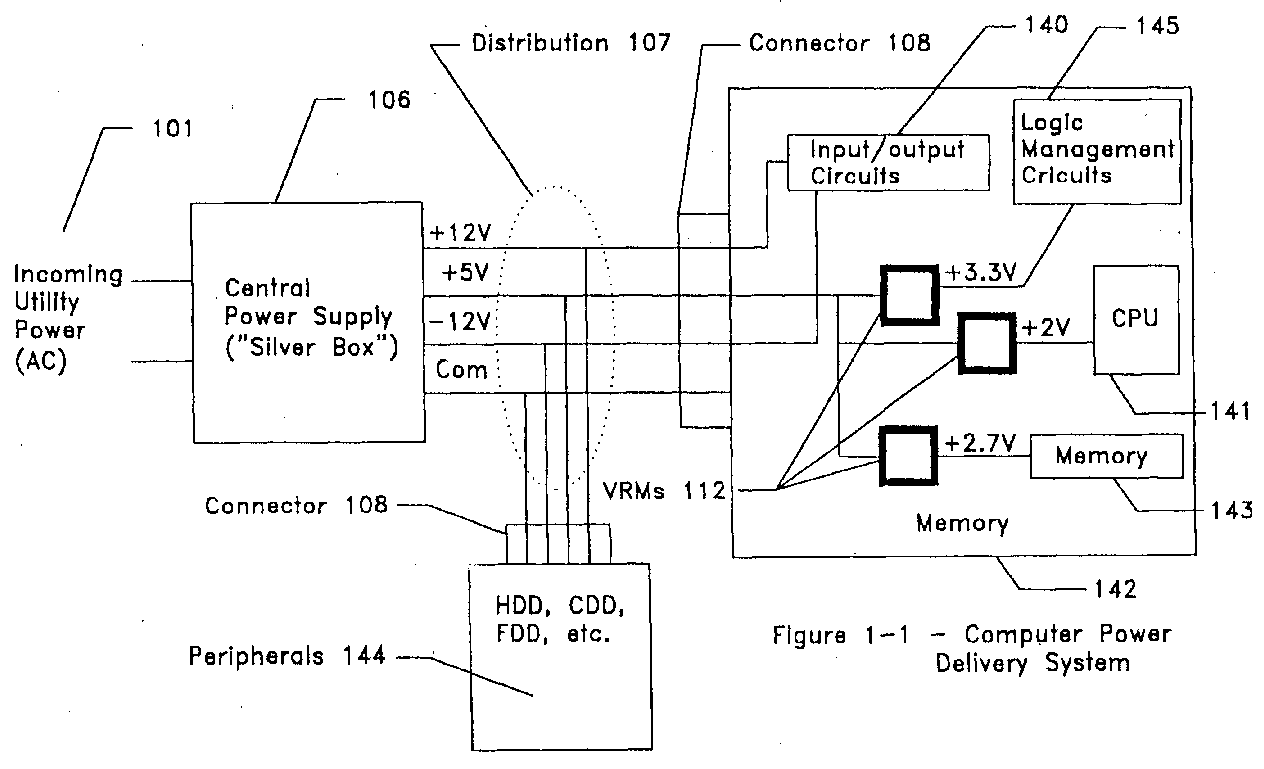
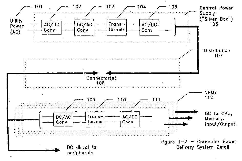


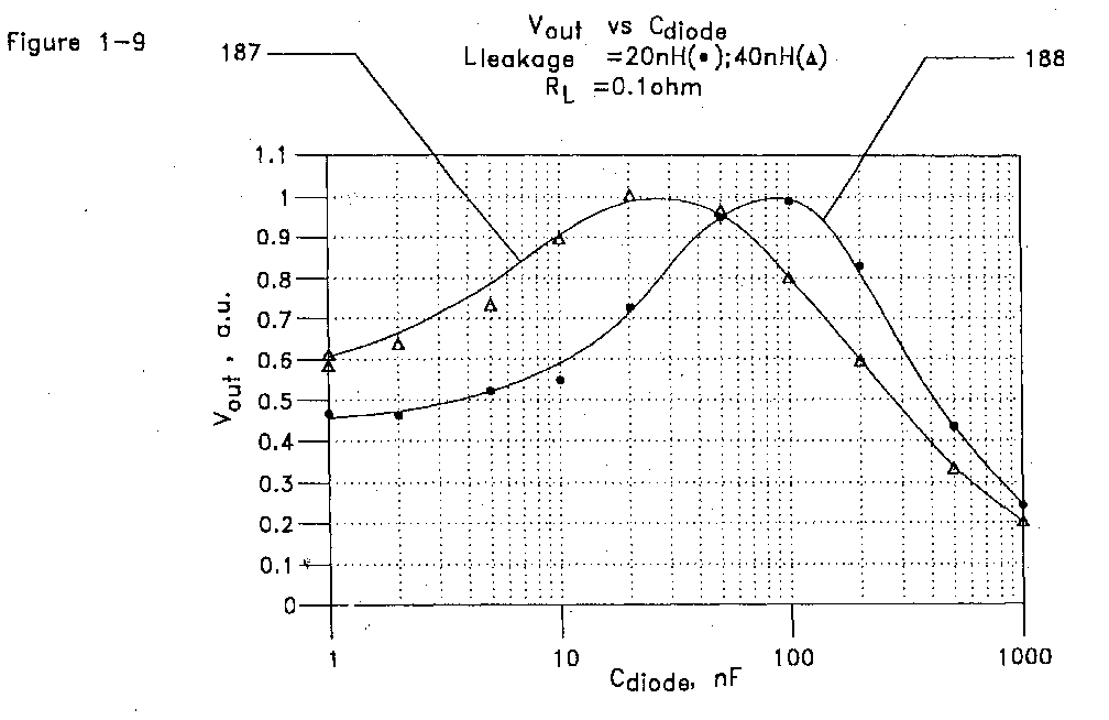


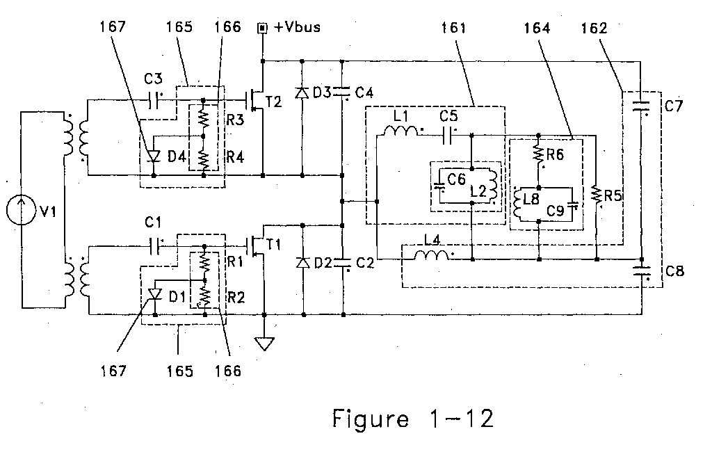
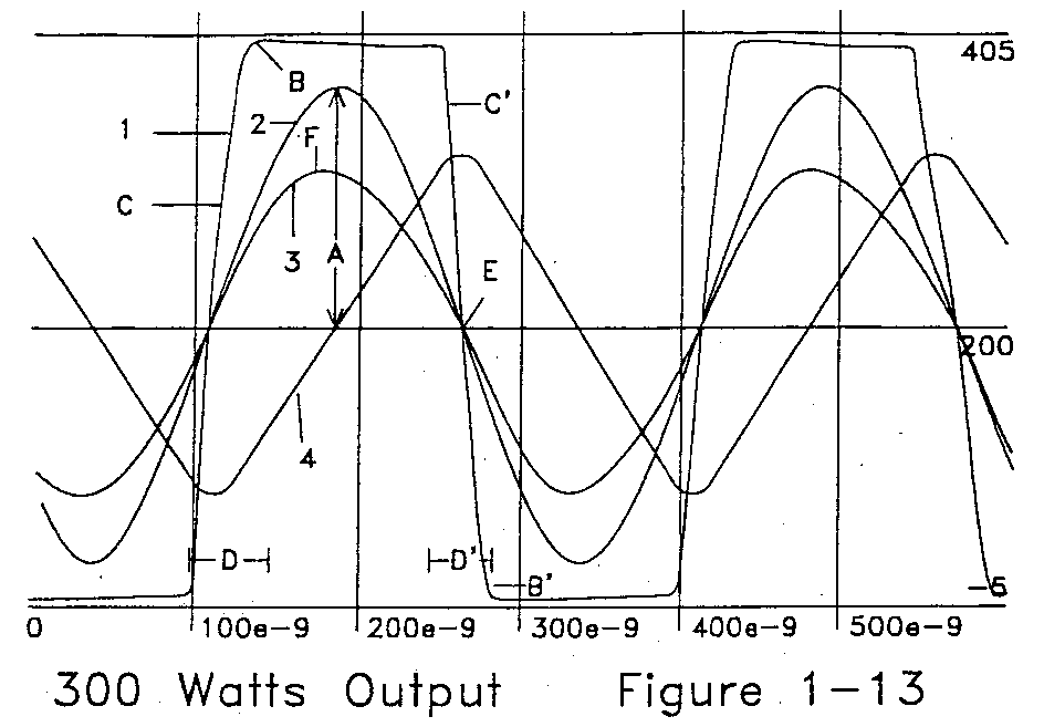
Description
- This invention is applicable for use in powering a wide variety of circuitry that requires low voltage and high current. In addition it provides capability to provide rapidly changing current. In particular it applies to microprocessors and similar circuitry especially where they are requiring less than 2 volts and are projected to require less than one volt.
- Buck converter topologies are in current use for powering microprocessors. For a 2.5 volt, 13 ampere requirement, a switching frequency of 300 kHz is becoming inadequate. To meet substantial step load changes a large output capacitance is becoming required. As microprocessor voltage requirements move downward toward 1.0 volt at 50 amperes, the prior art topologies become even less suitable. With a drop in voltage (and an attendant drop in differential voltage tolerance) of 2.5 times, and an increase of current of 4 times, a larger output capacitor is now needed to maintain the required step response. It becomes increasingly difficult or impossible, however, to locate such a large capacitor close to the microprocessor connections. In addition, the cost of this approach increases with decreasing voltage. One solution to this problem has been to increase the frequency of the voltage regulation module. When the frequency increases in such an arrangement, however, the non-resonant edges of this waveform cause problems such as the commutation of FET output capacitance and prevent increasing the switching frequency above about a megahertz. This situation is rapidly becoming serious as microprocessors and other low voltage electronics are ting developed which are increasingly difficult to provide suitable power for. The present invention permits the achievement of power for such needs. It permits higher frequencies and can be configured to handle higher currents.
- This situation is rapidly becoming serious as microprocessors and other low voltage electronics are being developed which are increasingly difficult to provide suitable power for.
- As mentioned, this invention specifically relates to powering computer systems. Here, often switch-mode DC is created to power the internal components of the system. It has particular applicability in new designs where microprocessors have high demands and power changes. Such can relate to the area of powering low voltage, high current electronics. As mentioned, though, the invention is applicable in the field of computing, and much of the following description is presented in that context. It should be understood, however, that other embodiments are in no way limited to the field of computing, and are applicable to a wide variety of circumstances wherein a variety of power absorbing loads which absorb electrical power may abruptly change their power absorbing characteristics (that is to say, their impedance may undergo a rapid change). They are also applicable if such loads are separated physically such that the voltage which may be dropped across the dynamic impedance of the power carrying conductors is a significant fraction of the voltage delivered to such loads. They are also increasingly applicable to applications wherein design tradeoffs are forcing a steady decrease in operating voltages. Such situations may arise in telecommunications, radar systems, vehicle power systems and the like, as well as in computing systems. Further, the DC/AC converter itself may have applications in broader and other contexts as well.
- The architecture of computing systems has undergone tremendous changes in the recent past, due principally to the advance of microcomputers from the original four-bit chips running at hundreds of kilohertz to the most modern 32 and 64 bit microprocessors running at hundreds of megahertz. As the chip designers push to higher and higher speeds, problems arise which relate to thermal issues. That is, as the speed of a circuit is increased, the internal logic switches must each discharge its surrounding capacitance that much faster. Since the energy stored in that capacitance is fixed (at a given voltage), as the speed is increased, that energy, which must be dissipated in the switches, is dumped into the switch that many more times per second. Since energy per second is defined as power, the power lost in the switches therefore increases directly with frequency.
- On the other hand, the energy stored in a capacitance increases as the square of the voltage, so a capacitor charged to two volts will store only 44% of the energy stored in that same capacitor charged to three volts. For this reason, a microcomputer designed to operate at two volts will, when run at the same speed, dissipate much less power than the same microprocessor operating a three volts. So there is a tendency to lower the operating voltage of microprocessors.
- Other considerations cause the microprocessor to exhibit a lower maximum speed if operated at a lower voltage as compared to a higher operating voltage. That is, if a circuit is operating at full speed, and the voltage on that circuit is simply reduced, the circuit will not operate properly, and the speed of the circuit (the "clock speed") may have to be reduced. To maintain full speed capability and still operate at lower voltage, the circuit often must be redesigned to a smaller physical size. Also, as the size of the circuitry is reduced, and layer thickness is also reduced, the operating voltage may need to be lowered to maintain adequate margin to avoid breakdown of insulating oxide layers in the devices. For the past few years, these steps have defined the course of microprocessor design. Key microprocessor designers, seeking the maximum speed for their products, have therefore expended considerable effort trading off the following considerations:
- higher speed chips are worth more money;
- higher speed chips must dissipate more heat;
- there are limitations to removal of that heat;
- lower voltages reduce the heat generated at a given speed; and
- smaller devices run faster at a given voltage.
- Of course, there are many, many important trade-off considerations beyond these, but the above list gives the basic elements which relate to some aspects of the current invention. The result of these considerations has been for the microprocessor designers to produce designs that operate at lower and lower voltages. Early designs operated at five volts; this was reduced to 3.3. to 3.0, to 2.7, to 2.3, and at the time of writing the leading designs are operating at 2.0 volts. Further reductions are in store, and it is expected that future designs will be operated at 1.8, 1.5, 1.3, 1.0, and even below one volt, eventually perhaps as low as 0.4 volts.
- Meanwhile, advances in heat removal are expected to permit processors to run at higher and higher heat dissipation levels. Early chips dissipated perhaps a watt; current designs operate at the 30 watt level, and future heat removal designs may be able to dissipate as much as 100 watts of power generated by the processor. Since the power dissipated is proportional to the square of the operating voltage, even as the ability to remove heat is improved, there remains a tendency to run at lower operating voltages.
- All of this is driven by the fundamental consideration: higher speed chips are worth more money. So the designers are driven to increase the speed by any and all means at their disposal, and this drives the size of the chips smaller, the voltages lower, and the power up. As the voltage drops the current increases for a given power, because power is voltage times current If at the same time improvements in heat removal permit higher powers, the current increases still further. This means that the current is rising very rapidly. Early chips drew small fractions of an ampere of supply current to operate, current designs use up to 15-50 amperes, and future designs may use as much as 100 amperes or more.
- As the speed of the processors increase, the dynamics of their power supply requirements also increase. A processor may be drawing very little current because it is idling, and then an event may occur (such as the arrival of a piece of key data from a memory element or a signal from an outside event) which causes the processor to suddenly start rapid computation. This can produce an abrupt change in the current drawn by the processor, which has serious electrical consequences.
- Inductance is the measure of energy storage in magnetic fields. All current-carrying conductors have associated with their current a magnetic field, which represents energy storage. It is well known by workers in the art that the energy stored in a magnetic field is half the volume integral of the square of the magnetic field. Since the field is linearly related to the current in the conductor, it may be shown that the energy stored by a current carrying conductor is proportional to half the square of the current, and the constant of proportionality is called the "inductance" of the conductor. The energy stored in the system is supplied by the source of electrical current, and for a given power source there is a limit to the rate at which energy can be supplied, which means that the stored energy must be built up over time. Thus the presence of an energy storage mechanism naturally slows down a circuit, as the energy must be produced and metered into the magnetic field at some rate before the current can build up.
- The available voltage, the inductance, and the rate of change of current in a conductor are related by the following equation, well known by those skilled in the art:
- Normally, in powering semiconductor devices one does not need to consider the inductance of the connections to the device, but with modem electronics, and especially with microprocessors, these considerations force a great deal of attention to be brought to lowering the inductance of the connections. At the current state of the art, for example, microprocessors operate at about two volts, and can tolerate a voltage transient on their supply lines of about 7%, or 140 millivolts. These same microprocessors can require that their supply current change at a rate of at least one-third or even nearly one ampere per nanosecond, or 3*108 or 109 amperes/second, respectively. The above equation indicates that an inductance of about 140 picohenries (1.4*10-10 H) and ½ nanohenry, (5*10-10 H) will drop a voltage of 140 millivolts at these two rates of current rise. To put this number in perspective, the inductance of a wire one inch in length in free space is approximately 20 nanohenries, or 20,000 picohenries. While the inductance of a connection can be reduced by paralleling redundant connections, to create a connection with an inductance of 140 picohenries with conductors about a centimeter long would require some 20 parallel conductors, and for instance a connection with an inductance of ½ nanohenry would require nearly 100 parallel conductors.
- The foregoing discussion implies that the source of low voltage must be physically close to the microprocessor, or more generally the active portion of a particular component, which in turn implies that it be physically small. While it might be suggested that capacitors might be used to supply energy during the delay interval required for the current in the conductors to rise, the intrinsic inductance of the connections to the capacitors currently severely limits this approach. So the system designer is faced with placing the source of power very close to the processor to ensure that the processor's power source is adequately stable under rapid changes in current draw. This requirement will become increasingly severe as the voltages drop still further and the currents increase, because the former reduces the allowable transient size and the latter increases the potential rate of change of current. Both factors reduce the permissible inductance of the connection. This can force the designer to use smaller capacitors which have low inductance connections, and because the smaller capacitors store less energy, this drives the power system to higher frequencies, which adds costs and lowers efficiency.
- The foregoing remarks are not limited in computers to the actual central microprocessor. Other elements of a modem computer, such as memory management circuits, graphic display devices, high speed input output circuitry and other such ancillary circuitry have been increased in speed nearly as rapidly as the central processing element, and the same considerations apply.
- Many modem electronics circuitry, including computers, are powered by switchmode power conversion systems. Such a system converts incoming power from the utility line to the voltages and currents required by the electronic circuitry by operation of one or more switches. In low power business and consumer electronics, such as desktop personal computers, the incoming power is supplied as an alternating voltage, generally 115 volts in the United States, and 220 volts in much of the rest of the world. The frequency of alternation is either 50 or 60 Hertz, depending upon location. Such utility power must be converted to low voltage steady (direct) current, or dc, and regulated to a few percent in order to be useful as power for the electronic circuits. The device which performs such conversion is called a "power supply". While it is possible to create a low voltage regulated DCpower source using simple transformers, rectifiers, and linear regulators, such units would be heavy, bulky and inefficient. In these applications it is desirable to reduce weight and size, and this approach is unsuitable for this reason alone. In addition, the inefficiency of linear regulators is also unacceptable. Efficiency is defined as the ratio of output power to input power, and a low efficiency implies that heat is being developed in the unit which must be transferred to the environment to keep the unit cool. The lower the efficiency the more heat must be transferred, and this is itself a reason for finding an alternate approach.
- For these reasons, virtually all modem electronics circuitry is powered by switchmode conversion systems. These systems typically operate as follows. The incoming utility power is first converted to unregulated direct current by a rectifier. The rectified DCis then converted to a higher frequency, typically hundreds of kilohertz, by electronic switches. This higher frequency power is then transformed by a suitable transformer to the appropriate voltage level; this transformer also provides isolation from the utility power, required for safety reasons. The resulting isolated higher frequency power is then rectified again, and filtered into steady direct current for use by the electronics. Regulation of the output voltage is usually accomplished by control of the conduction period of the electronic switches. The 5 resulting power conversion unit is smaller and lighter in weight than earlier approaches because the size and weight of the transformer and output filter are reduced proportionally to the increase in frequency over the basic utility power frequency. All of this is well known in the prior art.
- In a complex electronic system, various voltages may be required. For example, in a computer system the peripherals (such as disk drives) may require +12 volts, some logic circuits may require +5 volts, input/output circuits may additionally require -12 volts, memory interface and general logic may require 3.3 volts, and the central microprocessor may require 2 volts. Standards have developed so that the central power source (the device that is connected directly to the utility power) delivers ±12 and +5 volts, and the lower voltages are derived from the +5 supply line by additional circuitry, called voltage regulation modules, or VRMs, near to the circuits that require the lower voltage. These additional circuits convert the +5 volt supply to high frequency AC power again, modifying the voltage through control of the period of the AC power, and again re-rectifying to the lower voltage dc.
- The resulting overall system is complex and not very efficient, in spite of the use of switchmode technology. In a typical 200 watt computer system, four watts are lost in the initial rectification of the utility line, eight watts in the electronic switches, 2.5 watts in the transformer, 20 watts in the output rectification and filtering, and four watts in the connections between the center power supply and the electronics boards. Thus 38.5 watts are lost in the conversion process for the higher voltage electronic loads. Substantial additional losses may be sustained in the low voltage conversion process. A typical 50 watt voltage regulation module, which may convert +5 volts at 10 amperes to +2 volts at 25 amperes for the microprocessor, will itself have losses of about one watt each in the AC conversion and transformer, and ten watts in the final rectification and filtering. Other voltage regulation modules will have losses almost as great, resulting in losses for the entire system which may be one-third of the power used. Some particularly inefficient approaches may demonstrate efficiencies as low as 50%, requiring that the input power circuits utilize twice the power required by the actual final circuitry, and requiring that twice the heat be dissipated in the electronics (which must be removed by a fan) as is theoretically required by the actual operating circuitry.
- This system evolved over the years and is not optimum for many current uses, but persists because of inertia of the industry and because of the perceived benefit of maintaining industry standards on voltages and currents as generated by the central power unit.
- An analysis of current trends in the microprocessor industry clearly indicates that the current system will not be adequate for the future. These trends show that the current draw of critical elements such as the core microprocessor has been steadily increasing and will continue to do so into the future. Meanwhile, the operating voltage has been steadily decreasing, dropping with it the allowable tolerance of the supply voltage in absolute terms. Finally, the rate of change of processor current - the current slew rate - is increasing very rapidly, with substantial additional increases forecast for the near future. All of these factors mitigate against the current technology and require a new approach to be adopted in the future. It has been reliably estimated that the current powering and other technology will not last more than one additional generation of microprocessors, and since designers are currently at work on the generation following the next, it can be said that these designers are in the process of developing a microprocessor which cannot be powered by currently available technology.
- A further problem in the prior art is the use of square wave electronic conversion techniques. Such technology, known as PWM, for Pulse Width Modulation, produces switch voltage waveforms which have steeply rising edges. These edges produce high frequency power components which can be conducted or radiated to adjacent circuitry, interfering with their proper operation. These high frequency power components may also be conducted or radiated to other electronic equipment such as radio or television receivers, also interfering with their proper operation. The presence of such components requires careful design of the packaging of the power system to shield other circuitry from the high frequency power components, and the installation of expensive and complex filters to prevent conduction of these components out of the power supply package on its input and output leads. What is needed then, is a power conversion system which enables small, highly efficient voltage regulation modules to be placed close to the point of power use, which is fast overall, and which is itself efficient and at least as low in cost as the prior art technology it replaces.
- It is an object of the present invention, therefore, to provide a means for storing energy with lower inductance connections than could be achieved with the prior art. It is a further object of the present invention to provide a source of energy at low voltage and high current which does not need to be placed in very close proximity to the electronic load. Similarly, it is yet an another object of the invention to provide a source of low voltage which can sustain the voltage across the powered load even in the presence of high rates of change of current draw
- It is also an object of the present invention, to provide a means of converting utility power to high frequency alternating power for efficient distribution at higher efficiency than can be achieved using existing techniques. It is also an object to provide a means of converting high frequency AC power to the low DCvoltages and high DCcurrents required by current and future electronics at higher efficiency than can be achieved using current techniques. It is another object of the present invention to maintain that efficiency over a wide range of load conditions.
- A further object of the present invention is to provide a source of high frequency power which is substantially smaller than that of the prior art. Similarly it is an object to provide a source of low voltage at high current which is substantially smaller than that of the prior art to permit such a source to be placed in very close proximity to the electronic load.
- It is also an object of the preset invention to provide closer control of the output voltage of a power source, even for extremely short time periods. That is to say, it is an object to ease the task of the powering or of providing a power source so that it does not need such wide bandwidth and has a small transient response to changes in load. Thus an object is to provide a system with better transient response to changes in load
- It is a further object of the invention to provide a power conversion system which stores less energy than that required by the prior art.
- It is additionally an object of the present invention to provide a power conversion system which can be produced at lower cost than the prior art.
- It is also an object to address problems associated with the use of square wave electronic conversion techniques. It is yet another object of the invention to reduce possible interference between the power system and the electronics being powered, as well as with other devices in the vicinity of the powered electronics, by reducing the rate of rise of currents and the rate of fall of voltages in the power system. Similarly, an object is to provide power using smoothly varying waveforms in the power conversion circuitry.
- It yet a further object of one embodiment of the present invention provide to power with the aforesaid objects being satisfied, yet operate at either a constant frequency or, through other embodiments, to accommodate variable frequencies as well.
- Another fundamental aspect of the invention is the potential for the affirmative use of the transformer leakage inductance. This can be necessary as the DC output voltage requirement is lowered.
- Another benefit of this invention involves the very nature of a power source. By incorporating some or all these elements it can be possible to provide power remotely. By making the output capacitance consist of only the bypass capacitors necessary on the microprocessor pins, the circuit feeding the microprocessor assembly can have essentially an inductive output.
- Several features will be disclosed which taken together or separately can allow the power conversion frequency to be increased to provide a low stored energy approach to meet the high di/dt requirements for next generation low voltage requirements. Thus, yet other objects include providing a circuit and method for providing power to electronics with low voltage, high current and high di/dt requirements, providing substantially higher power conversion frequencies, providing a circuit which allows a reasonable amount of transformer leakage inductance and switching device capacitances, providing a circuit or method whereby the synchronous rectifiers (SR's) always switch with zero voltage across the device, allowing high frequency operation, providing a circuit or method whereby the control signal to the SR operates in a non-dissipative fashion, allowing HF operation, and providing a reduced size of the output capacitance through HF operation.
- Accordingly, in one embodiment the present invention is directed to a system of energy storage which can store more energy and be placed physically farther from the powered electronics, through the reduction of magnetic fields surrounding the electrical connections and the magnetic energy stored therein, thereby creating a faster responding circuitry, and simplifies the design and reduces the cost of the line filters used to avoid conducted interference along the utility power lines. Also, distribution of low DCvoltages (e.g., 5 volts) results in relatively higher losses in the distribution wires and connectors when compared to the use of medium voltage alternating distribution levels (e.g., 30 volts rms), which nevertheless remain safe to touch.
- According to the present invention there is provided:
- A DCpowered computer system comprising:
- a. a utility power input which supplies AC utility power having a line frequency,
- b. a line voltage rectifier element which converts said AC utility power to a DCsignal;
- c. an inverter element responsive to said DCsignal which establishes an alternating power output;
- d. a frequency driver which controls said inverter element to establish a distribution frequency;
- e. a supply transformer element which is responsive to said alternating power output and which establishes at least one distribution output at least one distribution voltage;
- f. a power distribution system responsive to said supply transformer element and which provides computer components power at locations electrically remote from said inverter element;
- g. at least one electrically remote voltage regulation
module responsive to said power distribution system
comprising;
- 1) an alternating power input;
- 2) at least one voltage regulation module transformer which is responsive to said alternating power input;
- 3) a first switched voltage regulation module rectifier element responsive to said voltage regulation module transformer element;
- 4) a second switched voltage regulation module rectifier element responsive to said voltage regulation module transformer element;
- 5) a passive rectifier control to which said first and said second switched voltage regulation module rectifier elements are responsive;
- 6) a bias input to which said passive rectifier control is responsive;
- 7) a second harmonics trap which is responsive to said first and said second voltage regulation module rectifier elements; and
- 8) a substantially non-capacitive DCoutput system which is responsive to said second harmonics trap; and
- h.. at least one computer component responsive to said DCsupply output.
-
- Said computer component responsive to said remote power DCsupply system may comprise a component operating at a nominal DCvoltage selected from a group consisting of less than about 2 volts, less than about 1.8 volts, less than about 1.5 volts, less than about 1.3 volts, less than about 1 volt, and less than about 0.4 volts.
- Said computer component may be capable of a rapid current demand which rises at a level selected from a group consisting of at least about 0.2 amperes per nanosecond, at least about 0.5 amperes per nanosecond, at least about 1 ampere per nanosecond, at least about 3 amperes per nanosecond, at least about 10 amperes per nanosecond, and at least about 30 amperes per nanosecond.
- Said computer component may comprise a component operating at a maximum current selected from a group consisting of more than about 15 amperes, more than about 20 amperes, more than about 50 amperes, and more than about 100 amperes.
- Said passive rectifier control to which said first and said second switched voltage regulation module rectifier elements are responsive may comprise an alternating control input.
- Said alternating control input may comprise a sinusoidal drive system to which said first switched voltage regulation module rectifier element and said second switched voltage regulation module rectifier element are responsive.
- Said voltage regulation module may further comprise:
- a. a first rectifier inductive output responsive to said first switched voltage regulation module rectifier element;
- b. a second rectifier inductive output responsive to said second switched voltage regulation module rectifier element; and
- c. a rectifier junction responsive to both said first rectifier inductive
output and said second rectifier inductive output, and
wherein said second harmonics trap comprises a parallel inductor and parallel capacitor connected to said rectifier junction. -
- Said voltage regulation module may further comprise an alternating input voltage regulator to which said voltage regulation module transformer is responsive.
- Said alternating input voltage regulator may comprise a variable capacitor.
- Said alternating input voltage regulator may comprise a series switch element.
- Said series switch element may comprise two switch elements.
- Said alternating input voltage regulator may comprise a regulator isolation element
- Said two switch elements may comprise switch elements driven at about a 180 degree phase relationship.
- Said voltage regulation module may further comprise a DCoutput coupling responsive to both said first rectifier inductive output and said second rectifier inductive output
- Said voltage regulation module may further comprise a third harmonics trap.
- Said voltage regulation module transformer may have a primary side and wherein said third harmonics trap comprises a third harmonics trap electrically tied to said primary side of said voltage regulation module transformer element
- According to another aspect of the invention there is provided a method of powering a DC computer system comprising the steps of:
- a. supplying an AC utility power having a line frequency;
- b. rectifying said AC utility power to a DC signal;
- c. inverting said DC signal to establish an alternating power output;
- d. distributing power to an electrically remote location;
- e. establishing a component DC supply voltage;
- f. transmitting said component DC supply voltage to an electrically remote computer component; and
- g. powering said computer component from said component DC supply voltage.
-
- Said step of transmitting said component DC supply voltage to an electrically remote computer component may comprise the step of transmitting said component DC supply voltage to over a distance selected from a group consisting of over at least about one-half inch, over at least about one inch, and over at least about two inches.
- Said step of transmitting said component DC supply voltage may comprise the step of transmitting said component DC supply voltage at a nominal DC voltage selected from a group consisting of less than about 2 volts, less than about 1.8 volts, less than about 1.5 volts, less than about 1.3 volts, less than about 1 volt, and less than about 0.4 volts.
- Said step of transmitting a component DC supply voltage may comprise the step of transmitting a component DC supply voltage through a DC output system capable of a rapid current demand which rises at a level selected from a group consisting of at least about 0.2 amperes per nanosecond, at least about 0.5 amperes per nanosecond, at least about 1 ampere per nanosecond, at least about 3 amperes per nanosecond, at least about 10 amperes per nanosecond, and at least about 30 amperes per nanosecond.
- Said step of transmitting a component DC supply voltage may comprise the step of transmitting a component DC supply voltage through a DC output system operating at a maximum current selected from a group consisting of more than about 15 amperes, more than about 20 amperes, more than about 50 amperes, and more than about 100 amperes.
- Said step of transmitting said component DC supply voltage to an electrically remote computer component may comprise the step of transmitting said component DC supply voltage through a substantially non-capacitive DC output system.
- Said step of transmitting said component DC supply voltage through a substantially non-capacitive DC output system may comprise the step of transmitting said component DC supply voltage through a substantially non-capacitive DC output system having an effective capacitance selected from a group consisting of less than about 0.3 millifarads, less than about 0.5 millifarads, less than about 1 millifarads, less than about 3 millifarads, less than about 10 millifarads, about only the inherent capacitance of a response network, about only an inherent reactance of a component connector, about only an inherent capacitance of said computer component, about only a bypass capacitance of a microprocessor, and any permutations or combinations of the above.
- The method may further comprise the step of electrically isolating said alternating power output prior to accomplish said step of establishing a component DC supply voltage.
- Said step of electrically isolating said alternating power output may comprise the step of transforming said alternating power output at said electrically remote location.
- Said step of rectifying said AC utility power to a DC signal may comprise the step of driving at least one rectifier element using a drive input and further comprising the step of electrically isolating said drive input at said electrically remote location.
- Said step of distributing power to an electrically remote location may comprise the step of utilizing substantially sinusoidal alternating signal power.
- Said step of utilizing substantially sinusoidal alternating signal power may comprise the step of utilizing substantially sinusoidal alternating signal power operating at a frequency selected from a group consisting of a frequency greater than at least about 300 kHz, a frequency greater than at least about 500 kHz, a frequency greater than at least about 1 MHz, a frequency greater than at least about 3 MHz, a frequency greater than at least about 10 MHz, a frequency greater than at least about 30 MHz, a frequency coordinated with an inherent capacitance of a first and a second switched voltage regulation module rectifier, a frequency coordinated with an inherent capacitance of said computer component, a frequency coordinated with an inherent capacitance of a component connector, a frequency coordinated with an inherent capacitance of a sinusoidal drive system, and any permutations or combinations of the above.
-
- Figure 1-1 shows a conventional computer power delivery system of the prior art.
- Figure 1-2 is a more detailed depiction of a computer power delivery system of the prior art.
- Figure 1-3 indicates the parts of the computer power delivery system of the prior art that may be eliminated by the present invention.
- Figure 1-4 shows a computer power delivery system according to one embodiment of the present invention.
- Figure 1-5 indicates an embodiment of the power conversion element of the present invention.
- Figure 1-6 depicts another embodiment of the power conversion element of the present invention.
- Figure 1-7 shows details of a switch drive according to the present invention.
- Figure 1-8 shows a rectifier circuit of the present invention.
- Figure 1-9 shows a variation of output voltage with changes in the value of a capacitance in one embodiment.
- Figures 1-10 and 1-11 show two variations of the voltage across a load resistance as a function of the load resistance.
- Figure 1-12 shows another embodiment with a two switch configuration and various general elements.
- Figures 1-13 and 1-14 are plots of voltage waveforms at various locations for two different loads, high and low respectively.
- Figure 3-1 shows a traditional buck converter of the prior art.
- Figure 3-2 shows a waveform of the center point of the buck converter shown in Figure 3-1.
- Figure 3-3 shows an embodiment of a transformer and rectifier portion according to the present invention.
- Figure 3-4 shows the voltage waveforms as they may exist at various locations in the circuit shown in Figure 3-3.
- Figure 3-5 shows one gate drive embodiment for the SR's according to the present invention.
- Figure 3-6 shows a circuit for voltage control on the primary side with a single switching design.
- Figure 3-7 shows a family of drain to source voltages as a function of the control input voltage across the FET.
- Figure 3-8 shows a circuit for voltage control on the primary side with a dual switching design.
- Figures 3-9 a, b, c & d shows various synchronous rectification circuits according to the invention.
- Figure 3-10 shows a bulk capacitor and a by pass capacitor arrangement as applied to a microprocessor system in the prior art.
- Figure 3-11 shows an overall preferred embodiment of the invention using a single switch control element.
- Figure 3-12 shows an overall preferred embodiment of the invention using a dual switch control element.
- Figure 3-13 shows an overall preferred embodiment of important aspects of the aspect of the design.
- Figure 3-14 shows yet another preferred embodiment of a voltage regulation module design using a variable capacitor for primary side regulation.
- Figure 3-15 is a Smith chart showing a range of VRM input impedances vs load current percentage for one design of the present invention.
-
- As can be easily understood, the basic concepts of the present invention may be embodied in a variety of ways. These concepts involve both processes or methods as well as devices to or which accomplish such. In addition, while some specific circuitry is disclosed, it should be understood that these not only accomplish certain methods but also can be varied in a number of ways. Importantly, as to all of the foregoing, all of these facets should be understood to be encompassed by this disclosure.
- Figure 3-5 shows one gate drive embodiment for the SR's according to the present invention.
- Figure 3-6 shows a circuit for voltage control on the primary side with a single switching design.
- Figure 3-7 shows a family of drain to source voltages as a function of the control input voltage across the FET.
- Figure 3-8 shows a circuit for voltage control on the primary side with a dual switching design.
- Figures 3-9 a, b, c & d shows various synchronous rectification circuits according to the invention.
- Figure 3-10 shows a bulk capacitor and a by pass capacitor arrangement as applied to a microprocessor system in the prior art.
- Figure 3-11 shows an overall preferred embodiment of the invention using a single switch control element.
- Figure 3-12 shows an overall preferred embodiment of the invention using a dual switch control element.
- Figure 3-13 shows an overall preferred embodiment of important aspects of the aspect of the design.
- Figure 3-14 shows yet another preferred embodiment of a voltage regulation module design using a variable capacitor for primary side regulation.
- Figure 3-15 is a Smith chart showing a range of VRM input impedances vs load current percentage for one design of the present invention.
- As can be easily understood, the basic concepts of the present invention may be embodied in a variety of ways. These concepts involve both processes or methods as well as devices to or which accomplish such. In addition, while some specific circuitry is disclosed, it should be understood that these not only accomplish certain methods but also can be varied in a number of ways. Importantly, as to all of the foregoing, all of these facets should be understood to be encompassed by this disclosure.
- In the prior art, the central power supply provides several standard voltages for use by the electronics. Referring to Figure 1-1, utility power (101), typically at 110 or 220 volt nominal AC power alternating at 50 or 60 cycles, is converted by power supply (106) to standard DCvoltages, usually ±12 and +5 volts. These voltages are brought out of the power supply on flying leads, which form a kind of distribution system (107), terminated in one or more connectors (108) These standard voltages are useful directly for powering most of the input/output circuitry (140) and peripherals (144), such as a hard disc, floppy disc, and compact disc drives. As the technology of central processing unit (CPU) chip (141) has advanced, as discussed above, the operating voltage of such chips has steadily been reduced in the quest for higher and higher operating speeds. This increase in processor speed eventually required an increase in speed of the dynamic random access memory (DRAM) chips (143) used to hold instructions and data for the CPU, and as a result the operating voltage of these DRAM chips has also been reduced. Also, not all of the logic required to manage the input/output functions and particularly the flow of data to and from the CPU and the memory and external devices is present on the CPU chip. These management functions, along with housekeeping functions (such as clock generation), interrupt request handling, etc., can be dealt with by the "chip set", shown in Figure 1-1 as logic management circuits (145). These circuits also have steadily increased in speed and have correspondingly required lower operating voltages.
- The standard voltages are thus too high to properly power CPU (141), memory (143), and management circuits (145). These may all require different voltages, as shown in Figure 1-1, where the actual voltages shown are representative only. These different voltages may each be created by an individual Voltage Regulation Module (112) (VRM), which may reduce the voltage supplied by the power supply (106) to the voltage required by the powered circuitry.
- From an overall point of view, the prior art process of delivering power to a circuit load such as CPU (141) involves all of the power processing internal to power supply (106), distribution system (107) and connectors (108), and the power processing internal to VRM unit (112). This overall process is shown in Figure 1-2. Central power supply (106), also called the "silver box", uses switchmode technology, with processing elements (102), (103), (104), and (105). The voltage regulation module (VRM) also uses switchmode technology. It should be understood that the discussion provided applies to both components. Thus the various features discussed in one context should be understood as potentially being applicable to the other. Focusing upon the silver box design only for purposes of initial understanding, it can be understood that utility power (101) enters the silver box and is converted to unregulated DCpower by rectifier unit, or AC/DC converter (102). The resulting
DCpower 5 is then re-converted to alternating current power at a higher frequency by inverter unit (103) (also called a DC/AC converter). The higher frequency AC is galvanically connected to and is at the voltage level of utility power (101). Safety considerations require isolation from utility power (101), and as the required output voltage is much lower than that of utility power (101), voltage reduction is also needed. Both of these functions are accomplished by transformer (104). The resulting isolated, low voltage AC is then rectified to direct or multiply direct current power output(s) by rectifier and filter unit (105), distributed to the circuitry loads by distribution wiring (107) and connectors (108). As mentioned before, specific standard voltages ±12 and +5 volts must be converted to lower voltages for CPU (141), memory (143) and management logic (145), by VRM unit (112). The standard DCvoltage from power supply unit (106) (usually +5 volts) is converted to alternating power again by DC/AC converter (109), transformed to the lower voltage by transformer (110), and re-rectified to the proper low voltage by AC/DC unit (111). - As the voltage of the delivered power to the circuit load is decreased, the current increases, and as the speed of CPU (141) is increased, the power system must be able to handle larger and larger rates of change of current as well. As discussed above, this requires the source of power, which for CPU unit (141) (and other low voltage circuits) is VRM (112), to be close to the circuit load. While for the near term designs the rate of change of current can be handled by capacitive energy storage, for future designs at still lower voltages and higher currents VRM unit (112) must be made extraordinarily small so that it can be placed close to its circuit load, and also must operate at a very high frequency so that large amounts of energy storage are not required. The requirement for low energy storage is rooted in the two facts that there is no physical room for the larger storage elements and no tolerance for their higher intrinsic inductance. Thus a requirement emerges that the frequency of VRM (112) must be increased.
- Further, a glance at Figure 1-2 indicates at least two redundant elements which can be eliminated. The established policy of distributing direct current power requires rectifier and filter (105), and the need for dropping the voltage to lower levels requires re-conversion of the DCto alternating current power by inverter (109). One of these is clearly redundant.
- This opens the possibility of reduction of cost by eliminating elements (105) and (109), and choosing to distribute alternating current power instead of direct current power. Of course, the AC improvement may also be configured with existing, traditional DCleads as well in a hybrid system if desired. Returning to the improvement, however, as mentioned before, the frequency of inverter (109) has had to increase and will continue to increase, which requires, in the reduced system, that the frequency of inverter (103) be increased to a level adequate to serve the future needs of the system. Figure 1-3 indicates these redundant elements.
- Another redundancy exists in principle, between transformers (104) and (110), but the desire to provide isolated power in the distribution system (107) mandates the use of transformer (104), and the requirement for different voltages for the different loads may also require the various VRMs to utilize transformer (110). Assuming that these elements are left in place, then, the use of high frequency AC distribution produces a system as shown in Figure 1-4. Thus one embodiment is directed specifically to the simplified VRM. Such an arrangement also permits electrically remote location of power element (e.g. at locations where the lead inductance would have otherwise have come into play using the prior techniques).
- In Figure 1-4, central power supply (147) converts utility power (101) to DCpower by AC/DC converter (146). This DCpower is then converted to high frequency sinusoidal power by DC/AC converter (113). The sinusoidal power (or perhaps "substantially" or "approximately" sinusoidal power, as may be produced by even a less than ideal inverter or the like) is distributed to the location of use of the power, where high frequency VRMs (118) convert the sinusoidal power to low voltage, high current power for the circuit loads such as CPU (141), input/output circuits (140), logic management circuits (145), and memory (143). In this approach, a VRM is required not only for the aforementioned low voltage circuits, but also for peripherals (144), since the DC power (likely +12 volt) requirement for these units is not supplied by the central power supply (106). (Note, the central power supply (106) may supply only sinusoidal high frequency AC power in this approach). High Frequency Transformer (114) may thus provide galvanic isolation and may transform the voltage from constant voltage Sinusoidal DC/AC Converter (113) to a level considered safe to touch.
- It is possible to organize a distribution system which provides a constant current to the totality of the loads, or alternatively to provide a constant voltage to those loads. The architecture of computer systems and other complex electronic systems with loads which require multiple voltages is more suited to the latter approach. That is, it is desirable that the magnitude of the distributed AC voltage be maintained very close to constant against any output load variation, even on a microsecond time scale. Thus, it can accommodate a variable load, namely a load which alters at levels which would have caused variation in the power supplied in arrangements of the prior art. It may also be important to keep the Total Harmonic Distortion (THD) of the distributed AC voltage low, to reduce Electro-Magnetic Interference (EMI). It should be noted, however, that the present invention may be modified to provide a constant current as well. That is, as those of ordinary skill in the art would readily understand, it is possible to modify the described circuit so that a constant current is delivered into a load which varies from nominal to a short circuit, for use in constant current applications.
- Converter (113) may be designed to provide a constant output voltage with low THD, independent of load Some of the embodiments presented herein depend upon being supplied with a constant input DCvoltage from converter (146). It would of course also be possible to create this constant distribution voltage by feedback internal to converter (113), as an alternative, which then would not require a constant input voltage from converter (146). The latter approach - creating constant voltage through feedback - requires that the feedback system have very high bandwidth (high speed) in order to maintain the output voltage very close to constant against any output load variation, even on a nanosecond time scale. This feedback approach may be difficult and expensive to achieve, and the present invention is directed to accomplishing a constant voltage from converter (113) by the intrinsic operation of the circuit, without feedback. This can be significant because it can satisfy the needs of a system which has rapid energy demands such as a rapid current demand of at least about 0.2 amperes per nanosecond, at least about 0.5 amperes per nanosecond, at least about 1 ampere per nanosecond, at least about 3 amperes per nanosecond, at least about 10 amperes per nanosecond, and even at least about 30 amperes per nanosecond and beyond. It also can be significant because it can permit reaction to a change in conditions very quickly, such as within:
- less than about a period of a "Nyquist frequency" (e.g. the Nyquist rate, that is the maximum theoretical rate at which sampling or transmission of an event can occur for a feedback-type of system),
- less than about two and a half times a period of a Nyquist frequency,
- less than about five times a period of a Nyquist frequency,
- less than about ten times a period of a Nyquist frequency,
- less than about twice a period of said alternating power output,
- less than about four times a period of said alternating power output,
- less than about 200 nanoseconds,
- less than about 500 nanoseconds,
- less than about 1000 nanoseconds, and
- less than about 2000 nanoseconds.
- Figure 1-5 shows one embodiment of a constant voltage high frequency power source to accomplish the function of converter (113). Here DCpower source (119) is the circuit representation of the constant voltage from converter (146), and load (128) represents the constellation of loads connected to distribution system (115) (including the effects of connectors (18) and distribution system) (115). The voltage from source (119) is converted to a constant current by inductor (120) and either shunted by switch (122) when the switch is ON, or permitted to flow into network (148), comprising the elements in parallel with switch (122) when the switch is OFF. The network thus acts as a response network, that is, one which acts after the switch has transitioned. The voltage across switch (122) is approximately zero when switch (122) is ON and is dependent upon the response of network (148) when switch (122) is OFF. This response waveform, or "switch voltage waveform" is transformed by network (48) to form the voltage across load (128). It turns out to be possible to choose the values of elements (123), (124), (125), (126), and (127) such that the switch voltage is zero at the commencement of the interval of time when switch (122) is ON, independent of the value of the conductance of load (128), at least within a nominal range of conductance for load (128). This may be accomplished in the following way. If the conductance of load (128) is very small (light loading), little current will flow in inductance (127), and its value will not strongly affect the waveform across switch (122). Then the values of elements (123), (124), (125), and (126) may be chosen to cause the waveform across switch (122) to be approximately zero, or to be a desired fixed value, at the moment when switch (122) begins to conduct. Clear descriptions for the methodology for accomplishing this may be found in U.S. patents 3,919,656 and 5,187,580. Once this has been accomplished, the conductance of load (128) may be changed to the maximum nominal value, and the value of inductor (127) chosen to return the value of voltage across switch (122 )at the commencement of its ON period to the value chosen in the first step. This algorithm will result in a circuit for which the value of the switch voltage waveform at the commencement of the ON period of switch (122) is nearly independent of the value of the conductance of load (128), within the defined nominal range. It also results in a circuit for which the shape of the switch voltage waveform varies minimally over the range of the conductance of load (128). A significant function ofthe network formed by elements (123), (124), (125), (126), and (127) is to form a sinusoidal waveform across load (128). Since this is a linear passive network, namely, a network with no active elements (including but not limited to steering diodes, diodes generally, other active elements, or the like) or a network without some type of feedback element (an element which senses a condition and then responds to that condition as a result of a delayed decision-type of result), if the shape of the switch voltage waveform does not change in any substantial way, and especially if the fundamental frequency component of the switch-voltage waveform (the Fourier component of the waveform at the operating frequency) does not change substantially, for this circuit the value of the sinusoidal voltage across load (128) will not change substantially. Thus selection of the values of elements (123), (124), (125), (126), and (127) in this manner results in a stable, constant, high frequency, pure sinusoidal voltage across load (128), independent of the value of the conductance of load (128), thereby accomplishing the objective of providing a constant voltage to the distribution system. It should be noted that the operation of this network to produce a constant output voltage is very fast; abrupt changes in the conductance of load (128) anywhere over its entire nominal range may be corrected in a few cycles of operation. This is much faster than typical feedback approaches could make the same correction and serves to provide a fast acting network, namely one which does not suffer the existing delay in a feedback type of system.
- A unique element of the invention is its high efficiency over the entire load range from a nominal load to an open circuit or from a nominal load to a short circuit. (As one skilled in the art should understand, one way to achieve one as opposed to the other simply involves altering the AC distribution system by one-quarter wavelength.) This comes about largely as 5 a result of the constant switch waveform described above. Since the voltage waveform changes but little over the load range, switching losses in the circuit are not affected by load variations. It should also be noted that all of the benefits of this invention are obtained without changing the frequency of operation. Thus, high efficiencies such as at least about 80%, at least about 85%, at least about 90%, at least about 95%, at least about 98% and even at least about 99% efficiency and beyond can be attained.
- Such a circuit, which provides a constant voltage sinusoidal output across a load (or even in not strictly "across" the load, more generically "to which the load is responsive" thus encompassing bit direct and indirect responsiveness) which can vary at high speed, utilizing a single or multiple switch and a simple circuit, operating at constant frequency, while maintaining high efficiency over the entire load range, is a unique aspect of this invention in the field of power conversion.
- Another unique element of the invention is in the nature of the method of driving switch (122). As has been pointed out previously, efficiency is important in these applications, and it is desirable not to waste energy anywhere, including the circuit used to drive switch (122). It is in the nature of high frequency switches such as Field Effect Transistors (FETs) that they have a large input capacitance. Circuits which change the voltage on the gate terminal in a square-wave manner must first charge that capacitance to a voltage well above the gate threshold voltage for switch (122), turning ON the FET, and in the process deposit energy into that capacitance. It must then discharge that capacitance to a voltage well below the gate threshold voltage for switch (122), in the process absorbing the energy stored in the gate capacitance. The power lost in the process is the energy stored in the gate capacitance, multiplied by the frequency of operation, and this can be a substantial number. In the present invention this loss is avoided by affirmatively utilizing the gate capacitance of switch (122), thus coordinating the circuitry to the gate or capacitance. That is, the energy stored in the gate capacitance during the period switch (122) is ON is, in the present invention, stored in another element of the system during the period switch (122) is OFF, and is thereby available on the next cycle to return the gate above the threshold voltage for the next ON period. This may be accomplished by "resonating" the gate capacitance (or the effective capacitance of the system) with a series or parallel inductor. The entire system may be tuned to coordinate with the frequency of the output and the output capacitance of the switch. Referring to Figure 1-7, FET switch (122) is depicted as an internal switch device (139) with an explicit gate capacitance (138), shown separately. Gate drive circuit (121), according to the current invention, contains inductor (136) connected in series (or in parallel as shown in the dotted-line alternate connection) (137) which is selected such that the reactance of inductor (136) or (137) is equal to the reactance of capacitor (138) at the 0 frequency of operation. In this way the energy in the gate system is transferred from gate capacitor (138) to inductor (136) (or its alternate) (137) and back again each cycle, and only the inevitable losses in the inductor and gate resistance need to be regenerated for each cycle.
- In such a system the gate voltage is substantially sinusoidal. It will be obvious to those skilled in the art that the duty cycle of the system (that is, the fraction of the total period that switch (122) is ON) is determined by the fraction of the sinusoidal cycle which is substantially above the threshold voltage of switch (122). It will also be obvious that, while the duty cycle of switch (122) may be controlled by the magnitude of the sinusoidal signal, such an approach places limits on the available range of duty cycle, and also may result in longer than desirable commutation times (that is, the fraction of the total period during which the switch is transitioning from the ON to the OFF state), which may increase the losses of switch (122) and thereby reduce the efficiency of the system. For this reason, the drive waveform for switch (122) may be divided in the present invention into an AC portion (149) and a DCportion (150), and variation in the duty cycle of switch (122) may be controlled by varying the relative magnitude of the AC and DCcomponents of the drive waveform for switch (122).
- An alternative approach to constant voltage, high frequency power generation is shown in Figure 1-6. Here again, DCpower source (119) is the circuit representation of the constant voltage from converter (146), and load (128) represents the constellation of loads connected to distribution system (115) (including the effects of connectors (108) and distribution system) (115). Switch (122) is placed in series with inductor (129), across source (119). The voltage across inductor (129) is transformed by transformer (131) and placed across the network comprised of elements (132), (133), (134), and (135). This network produces the output voltage appearing across load (128), which again represents the constellation of loads connected to distribution system (115) (including the effects of connectors (108) and distribution system) (115). Provided the values of the circuit elements are properly chosen, this output voltage will be independent of the value of the conductance of load (128), within a nominal range of such conductance. To create this independence, it is sufficient to select the values of the elements such that, as one example, the reactance of inductor (129) in parallel with the magnetizing inductance of transformer (131) is equal to the reactance of capacitor (130) in parallel with the adjunct output capacitance of switch (122) at the frequency of operation, the reactance of inductor (132) in series with the leakage inductance of transformer (131) is equal to the reactance of capacitor (133) at the frequency of operation; and the reactance of inductor (134) is equal to the reactance of capacitor (35) at the frequency of operation. Selection of the values of the circuit elements in this manner will result in a stable, constant, high frequency, pure sinusoidal voltage across load (128), independent of the value of the conductance of load (128), thereby accomplishing the objective of providing a constant voltage to the distribution system.
- The necessity for the parallel resonant circuit formed by inductor (134) and capacitor (135) is reduced if the minimum load conductance is not too close to zero. That is, the network comprised of elements (134) and (135) has the function of providing a minimum load to the generator so that the output waveform remains sinusoidal when load (128) is removed or reduced to a very low value. Should the application to which the invention is applied not present a load variation down to low values, or if the requirement for low THD not be present at light loads, the network comprised of elements (134) and (135) may be dispensed with Alternatively, the network comprised of elements (134) and (135) may be reduced to a single element, which may be either an inductor or a capacitor, if the highest efficiency is not demanded.
- It is generally possible to also dispense with inductor (129) by affirmatively utilizing the magnetization inductance of transformer (131). Similarly, it is generally possible to dispense with inductor (132) by affirmatively utilizing the leakage inductance of transformer (131). This may be accomplished through the modification of the construction of transformer (131) in the manner well known to those skilled in the art. As before, to attain high efficiency it is important to affirmatively utilize the gate capacitance of switch (122), and all the remarks made above in reference to Figure 1-7 apply to the embodiment of Figure 1-6 as well.
- As mentioned earlier, and referring to Figure 1-4,
converter 113, operating together with AC/DC element (146), is designed to provide a constant high frequency AC output voltage with low THD, independent of load. It is VRM (118) which must convert this high frequency AC power from power unit (147) to low voltage high current DC power for use by the powered circuitry (145), (141), and (143). Figure 1-8 shows one embodiment of the rectifier portion of one embodiment of a VRM to accomplish this conversion in accordance with the present invention. Input AC power from power unit (147) may also be processed further to enhance its stability before the rectification process, and this further processing is not shown in Figure 1-4. The result of this processing is a stable regulated AC input (177) to the rectifier circuit (178) shown in the dotted box in Figure 1-8. - Rectifier circuit (178) is comprised of transformer (179), which in practice will exhibit leakage inductance caused by imperfect coupling between its primary and secondary windings. This leakage inductance may be represented in general as an inductance in series with the primary or secondary of the transformer. In Figure 1-8, it is represented by inductor (180), which therefore may not be an actual component in the circuit, but rather simply a circuit representation of part of the real transformer (179), as built. It should be noted that, should the natural leakage inductance of transformer (179) be smaller than desirable for any reason, additional inductance may be added in series with its secondary (or primary) to increase the natural value, as will be understood by those skilled in the art. For the purposes of this disclosure, inductor (180) may be considered to be the total of the natural leakage inductance of transformer (179) and any additional discrete inductance which may have been added for any purpose.
- Diodes (83 )rectify the AC output of transformer (179), and filter inductors (184) and filter capacitor (185) create a steady DCoutput for consumption by the microprocessor or other electronic load (186). For small output voltages, the voltage drop across the diodes (183) is too large relative to the output voltage, resulting in loss of efficiency. As a result diodes (183) may be profitably replaced by field effect transistor (FET) switches, which can be manufactured to have a much lower voltage drop. In this case the FET devices require a drive signal to determine their conduction period; the circuitry to do this is not shown in Figure 1-8.
- A second problem which arises as the output voltage is dropped is the intrinsic leakage inductance of transformer (179). This inductance, which, together with other circuit inductance, is represented as inductor (180), and acts as a series impedance which increases the output impedance of the overall circuit. That is, there is a natural voltage division between the reactance of inductor (180) and load impedance (136), which requires an increased input voltage in compensation, if the output voltage is to remain constant over changes in the resistance of load (186). This voltage division causes the output voltage to be a strong function of the resistance of load (186), which is another way of saying that the output impedance of the circuit is not small compared to the load resistance (186).
- The diodes (183) shown in Figure 1-8 would ideally conduct whenever the voltage on their anodes was positive with respect to their cathodes, and would not conduct when the voltage was in the opposite polarity. This is what is called zero voltage switching, or ZVS, because the switching point, or transition, from the conducting to the nonconducting state occurs at zero voltage point in the waveform. Operating an FET device at ZVS is an advantage, because the losses are lowered, since the device does not have to discharge energy from its output capacitance, or the energy stored in capacitors (182), which are in parallel with the switches. As the output current through load (186) increases, the timing for the switches to produce ZVS must change, and may complicate the FET drive circuitry. In the description of the figures which follow, we shall nevertheless assume that the switches are operated at ZVS conditions, or that a true diode is used.
- Figure 1-9 shows how the output voltage varies with changes in the value of capacitance (182) placed across diodes (183). These curves were plotted for an operating frequency of 3.39 MHz. As may be seen in Figure 1-9, as the value of capacitances (182) are increased, the output voltage (that is, the voltage across load resistance) (186) first begins to increase, but as the value of the capacitance (182) is increased still further, the voltage across load resistance (186) begins to drop again. Thus there is an optimum value for the capacitances (182) which obtains the highest voltage transfer function. In Figure 1-9 two curves are shown, curve (187) a value of inductance (180) of 40 nH, and curve (188) for a value of inductance (180) of 20 nH. Curve (187) shows that a peak in output voltage occurs at a value for capacitances (182) of about 27 nF, while curve (188) shows that a peak occurs at a value for capacitances (182) of about 86 nF. Note that these are not a factor of two apart (86/27>3) as would be the case if the values of capacitances (182) and inductor (180) satisfied the resonance condition since the two curves are for values of inductor (180) which are a factor of two apart. This means that the condition for maximum output is not the same as for resonance at the frequency of the input power from generator (177). The two capacitors (180) may be replaced by a single capacitor (181) in a parallel position across the secondary winding of transformer (179) and inductor (180), with the same result, although the current in the diodes (183) will not be the same in this case.
- Figures 1-10 and 1-11 show the voltage across load resistance (186) as a function of the load resistance (186). The slope of these curves is a measure of the output impedance of the circuit (178). That is, if the slope is zero, the output impedance is zero, and the circuit exhibits "natural regulation" without feedback. Curve (189) in Figure 1-10 and curve (192) in Figure 1-11 show that, for a value for capacitances (182) equal to the value which results in a peak in voltage across load resistance (186), a slope of nearly zero is obtained, without feedback. That is, for a proper selection of the value of capacitances (182) in relation to inductance (180), the voltage across load resistor (186) becomes relatively independent of the actual value of the load resistor (186) - the output is "naturally regulated". It will be seen that the advantage of "natural regulation" - regulation without feedback - is that one does not need to wait for a feedback system to recognize a change in output voltage compared to a reference, and to change some parameter internal to the circuit. Under the described conditions, the output voltage is held constant and maintained so within a cycle or two of the operating frequency, which is short compared to stable feedback systems.
- Thus a system has been described which produces a stable output voltage over a wide range of load resistances without feedback, even under conditions of rapid change in the load resistance. For systems which can tolerate the change in output shown in the figures, no feedback is required. For systems which require tighter control of the output voltage under conditions of changing load, feedback may be added, and it will be noted that the teachings of the present invention reduce the requirement for action on the part of the feedback system, permitting simpler, faster, and less costly feedback circuits to be used.
- As mentioned earlier, the circuit can be embodied in a variety of manners to achieve the overall goals of this invention. For example, referring to Figure 1-12 as but one other example of a circuit design, in general, the circuit can be understood. It may have any combination of a variety more generically stated elements. First, it may have a constant output element, such as the constant output voltage element (161). In this arrangement, the constant output element serves to maintain some output parameter as a constant regardless of a variation such as may occur from the variable load. As one skilled in the art would readily understand, the parameter maintained may be selected from a great variety of parameters, including but not limited to parameters such as:
- a substantially constant switch voltage output which is substantially constant over all levels at which said variable load exists practically,
- a substantially constant load voltage input which is substantially constant over all levels at which said variable load exists practically,
- a substantially constant switch voltage Fourier transform which is substantially constant over all levels at which said variable load exists practically,
- a substantially constant switch voltage output waveform which is substantially constant over all levels at which said variable load exists practically,
- a substantially constant switch voltage transition endpoint which is substantially constant over all levels at which said variable load exists practically, and
- all permutations and combinations of each of the above
- Second, the system can include a constant trajectory element such as the constant trajectory element (162). In this arrangement, the constant trajectory element serves to maintain the response waveform (or even the Fourier component of the waveform) as substantially a constant regardless of a variation such as may occur from the variable load. In the configuration shown, this constant trajectory element (162) has inductor L4 connected to a half supply (shown as capacitors C7 & C8). It provides a constant current at the time of transition from switch T1 conducting or switch T2 conducting (or visa versa) where diode D2 and capacitor C2 are adjunct elements of switch T1, and diode D3 and capacitor C4 are adjunct elements of switch T2. The trajectory which is maintained may even be held to one which present a continuous second derivative of voltage with respect to time. As shown herein, designs may also be configured to achieve a constant end point. The end point may or may not be zero, for instance, it may be desirable in certain designs to have a non-zero end point. That type of a design may include values such as: zero volts, a voltage which is less than a diode turn-on level, less than about 5% of said switch DC supply voltage, less than about 10% of said switch DC supply voltage, less than about 20% of said switch DC supply voltage, and less than about 50% of said switch DC supply voltage, each over all levels at which said variable load exists practically. Regardless, a constant result (trajectory, end point, or otherwise) can be important since it is the voltage at the moment of switch turn-on or the avoidance of turning on the body diode which can be highly important. Again, from all these general principles, as a person of ordinary skill in the art would readily understand, other designs can be configured to achieve each of these basic goals. Designs may thus provide a network which is substantially load independent and which provides a substantially trajectory fixed response. Further, any nonlinear transfer characteristics of any component, such as the varactor capacitance nature of many switches, the nonlinear transfer characteristics of a transformer, or the like, can be affirmatively utilized by the network as well for an optimal result.
- Third, the circuit may include an energy maintenance element, such as the energy maintenance circuit (163). In this feature, the energy maintenance circuit (163) serves to maintain the energy needed as a constant regardless of a variation such as may occur from the variable load. In the configuration shown, this energy maintenance circuit (163) has a capacitor C6 configured in parallel with inductor L2, both being in parallel with the load shown as R5. This element may serve to supply substantially all of the rapid energy demand of the load such as discussed earlier. Again, as before other designs can be configured to achieve this basic goal.
- Fourth, the circuit may have some type of stabilizer element such as the stabilizer element (164) shown. This stabilizer element (164)serves to absorb energy not in the fundamental frequency in accordance with the principles discussed in US Patent No. 5,747,935, hereby incorporated by reference, to the assignee of the present invention.
- Finally, the circuit may include an automatic bias network such as the direct bias alteration element (165) as shown for each switch. In this arrangement, these networks may include some type of voltage divider (166) with a conduction control element such as diode (167). Here, the voltage divider (166) uses two resistors R1 & R2 which may be selected to be equal, each with high values such as 1k ohm. This element provides a negative bias in proportion to the AC drive amplitude. The result can be a conduction period which is independent of the drive amplitude. It can thus provide a constant dead time (response time) when neither switch is in the conductive state. Again, from these general principles, as a person of ordinary skill in the art would readily understand, other designs can be configured to achieve this basic goal as well.
- As illustrated in Figures 1-13 and 1-14, it can be seen how a properly configured system according to the present invention has the constancy features mentioned. The plots 1-4 show waveforms as follows:
- 1- the voltage at the junction between switches T1 and T2;
- 2- the output voltage across the load, R5;
- 3- the current through L1; and
- 4- the current through L4. By comparing the high load and low load situations for the same network as shown between the two figures, several events can be noticed. These include the constant output voltage (A), constant end point (B and B'), constant trajectory (C and C'), constant response time period (D and D'), zero voltage switching (B and B'), and constantly an event of zero load current in the transition (E), all even though there is a highly varying power and load current as indicated by the current into the network at L1 (F and F'). Other features are also noticeable, as one skilled in the art should easily understand.
-
- As mentioned earlier, buck converter topologies (such as shown in Figure 3-1) are in current use for powering microprocessors, especially for voltage regulation modules. For a 2.5 volt, 13 ampere requirement, a switching frequency of 300 kHz is becoming inadequate. To meet substantial step load changes an output capacitance (301) of 3 mF (millifarads) is becoming required. As microprocessor voltage requirements move downward toward 1.0 volt at 50 amperes, the prior art topologies become even less suitable. With a drop in voltage (and an attendant drop in differential voltage tolerance) of 2.5 times, and an increase of current of 4 times, an output capacitor of 30 mF would be needed to maintain the required step response. It becomes increasingly difficult or impossible, however, to locate such a large capacitor close to the microprocessor connections. In addition, the cost of this approach increases with decreasing voltage. The other possibility would be to increase the frequency. The voltage waveform (302) shown in Figure 3-2 is typical for a buck converter. When the frequency increases in such an arrangement, however, the non-resonant edges of this waveform cause problems such as the commutation of FET output capacitance and prevent increasing the switching frequency above about a megahertz. This situation is rapidly becoming serious as microprocessors and other low voltage electronics are being developed which are increasingly difficult to provide suitable power for. The present invention permits the achievement of higher frequencies and currents as will be required. It permits frequencies such as greater than at least about 300 kHz, greater than at least about 500 kHz, greater than at least about 1 MHZ, greater than at least about 3 MHZ, greater than at least about 10 MHZ, and even greater than at least about 30 MHZ and beyond, and can be configured to handle currents of more than about 15 amperes, more than about 20 amperes, more than about 50 amperes, and even more than about 100 amperes and beyond.
- In one embodiment, an aspect of this invention is the basic change from a circuit converting DCto DCto a circuit transforming ACto DCmaking use of a transformer and a synchronous rectifier. A transformer is useful in this approach as it is possible to eliminate large currents being distributed to the converter input. The high current secondary can thus be located physically close to the load. One circuit for accomplishing this shown in Figure 3-3. With the invention disclosed, the energy conversion frequency can be increased substantially, thereby allowing the output capacitance (303) to remain small and be located adjacent to a given load such as the microprocessor interconnections. In fact, much higher conversion frequencies can be achieved and whereby the output capacitance can be substantially reduced. In the case of the 1.0 volt, 50 ampere requirement, the output capacitance (303) with the present invention can be 500 µF or lower, depending upon load requirements. In fact, with the present invention, designs can be accomplished which provide a network having an effective capacitance (that which causes an appreciable effect in the use or circuit designed) which is less than about 10 millifarads, less than about 3 millifarads, less than about 1 millifarads, less than about 0.5 millifarads, and even less than about 0.3 millifarads.
- Such a dramatic improvement can come through the incorporation of several elements individually or simultaneously. One primary goal of this invention is the elimination of frequency related limitations. Consequently it can be important to eliminate forced voltage commutation of any capacitors. The Synchronous Rectifier (SR) (304) device used may be a Field Effect Transistor (FET) with adjunct drain to source capacitance (305). This SR can always be commutated to the conducting state at a time when there is zero voltage across it.
- Figure 3-3 shows a preferred embodiment for the rectification portion of a low voltage high current supply. The element LT (306) (total series inductance) is defined as the total of the transformer leakage inductance plus any other inductance in series with the transformer (inductance in the primary is simply scaled to the secondary). The element CT (total parallel capacitance) is defined as the total of the SR adjunct capacitance (305) (Coss), plus any external parallel capacitance of each SR (307) (Csr) plus any capacitance in parallel with the transformer secondary (308) (Cp).
- There are several parameters which may be considered to optimize this circuit If the load being powered has the possibility of high di/dt or if the load current can be a step function up or down then the following parameters could be considered:
- fundamental frequency of operation
- transformer turns ratio
- LT
- CT
- conduction angle (CA) for the SR's
- phase delay (PD) of the SR's
- Also to be potentially considered is the basic relationship between conduction angle and efficiency. In prior art and practice the conduction angle for the SR's has been carefully chosen to be less than or equal to 180 degrees (i.e., no SR conduction overlap) to prevent a short circuit on the transformer secondary. This common misperception arises from lower frequency assumptions. With the present invention, a conduction angle greater than 180 degrees is not only allowed but provides a fundamental benefit of operation. Conduction angles in the range of 300 degrees or higher are clearly demonstrated. With properly chosen LT, CT, phase angle (PA) and conduction angle (CA), the drain waveforms on the SR's (304) shown in Figure 3-4 can be realized. With these conditions, a low ratio of SR root-mean-square (RMS) current to output current can be realized. Ratios of<1.3:1 have been achieved.
- Just as a general comparison, the waveforms from Figure 3-4 can be compared to Figure 3-2 from the prior art. They both share the low duty cycle aspect but it is clear in Figure 3-4 the switching of the SR occurs at zero volts and is ideally lossless.
- The transformer leakage inductance is a fundamental limiting factor for low voltage, high current, high frequency power supplies. It consists of an inductance in series with the transformer and has historically limited the conversion frequency.
- In other art leakage inductance has been dealt with in various ways. Three patents, by Schlecht, Lee and Bowman, covering DCto DCconverters will be touched on as all include methods of handling the leakage inductance. In Schlecht et al., US Patent #4,788,634, the leakage inductance is managed by minimizing it As that patent states: "It is desirable to limit the size of this leakage inductance to a negligibly small value compared to the resonant inductor (in this case the transformer primary inductance) such that the unilateral conducting element and controllable switch both have zero voltage switching transitions." In Lee et al., US Patent # 4,785,387 and Bowman US Patent # 4,605,999 the transformer leakage inductance is used in a circuit resonant at or slightly above the fundamental frequency. The goal for this circuit is to accomplish zero voltage switching both for the primary switches as well as for the rectifiers. However, the present invention shows use of the leakage inductance in a manner not resonant at the fundamental frequency.
- One fundamental aspect of this invention is a circuit topology and class of operation which can make allowance for a larger leakage inductance. This benefit can be realized by the choice of a high conduction angle in the SR's. In fact, for some applications conduction angles even greater than 300 degrees are shown to be valuable. As the output voltage requirement is reduced and the current requirement is increased, both of these shifts result in still higher conduction angles. The setting of this large conduction angle, the total inductance and total capacitance is done simultaneously with one of the desirable conditions being Zero Voltage Switching (ZVS) for the synchronous rectifiers. This allows operation at a higher frequency or, at a given frequency operation with a higher leakage inductance. This 5 combination of high frequency operation and/or higher leakage inductance tolerance is a fundamental benefit of this design and may perhaps be a necessary benefit as microprocessor power requirements become more difficult to fulfill.
- One additional note with respect to the total capacitance - the choice of location between putting the capacitor across the transformer (308) or across the SR's (307) changes the current waveform through the SR's but does not greatly affect the voltage waveform. With the capacitor across the transformer makes the current waveform more like a square wave while it is quasi-sinusoidal when the capacitor is across the SR. This difference can have significant ramifications as those of ordinary skill in the art should readily understand to some degree.
- One general principal observed in rectifier circuit design is to minimize the reverse voltage stress across the rectifier device. Depending on the type of filter input the peak inverse voltage is usually in the range of being equal to the DC output voltage upwards to 1.4 times the output voltage or in rare circumstances up to twice the DC output voltage.
- One consequence though of the high conduction angle is substantially higher voltage across the rectifier devices. For example in the circuit values disclosed here the output voltage is 1.8 volts while the voltage across the rectifier devices is 15 volts! Historically this type of circuit performance has been thought of as poor practice for a variety of reasons as those of ordinary skill in the art well understand. Perhaps this is one reason why such a valuable circuit has not been discovered to date.
- But a high conductance angle with attendant high voltage across the SR during the non-conducting state has the benefit of low RMS current through the SR during the conducting state and is a condition for allowing large transformer leakage inductance. This circuit is ideally suited for low voltage, high current requirements. Furthermore it is well suited to loads which have a high di/dt requirement as a result of the higher operating frequency and lower stored energy in the output capacitance. As it turns out the higher voltage requirement for the SR's is not troublesome. With current manufacturing technology there appears to little benefit to restraining the SR off state voltage to less than about 20 volts.
- The next circuit being disclosed, Figure 3-5, is a gate drive circuit that derives its power from the ACinput and uses only passive elements. The gate drive of the SR's is also almost lossless. This all results in low cost and predictable performance. It is also important for higher frequency operation.
- In addition it is possible to add a DCor low frequency bias to provide regulation or improve efficiency under various load conditions. In Figure 3-5 the point labeled BIAS INPUT is an example of an injection point for the control input. Varying the voltage on this input has the effect of varying the conduction angle of the SR's without effecting the DELAY ANGLE (Figure 3-4).
- The correct phase angle for conduction of the SR's is determined by the gate drive. Referring to Figure 3-4, the angle labeled DELAY ANGLE could be derived by using something like elements L1, R1,2 and C1,2 of Figure 3-5. The inductance L1 includes the gate drive transformer leakage inductance.
- There could be many variations of gate drive which embody these principles. This may be contrasted with conventional technology in which the gate drive is derived from a DC source and involves timing circuitry and switching devices.
- It is possible to also control and/or regulate the output voltage by varying the SR Conduction Angle (CA). Consider Figure 3-3 again with the inclusion of the
capacitor Cin 309 shown in dotted lines. - To select values for the controlled output circuit, first examine the case where the CA goes to 360 degrees for the SR's. This results in a zero DC output The impedance of
Cin 309 should now be matched to the value of LT (transformed to the primary by the square of the turns ratio) forming a parallel resonant circuit at the fundamental frequency. As can now be seen the AC input is only loaded by a parallel resonant circuit which in the ideal condition is lossless. - There exists a continuum of CA's from 360 degrees downward until the full load condition is reached as before. With properly chosen circuit parameters ZVS switching can be maintained over the whole regulation range. One important requirement for ZVS is to provide constant phase relationship between conduction time and the ACinput. In the first order analysis, the only control input required is that shown in Figure 3-5.
- Another method of providing regulation or control of the output could be to use parametric elements such as a varactor capacitor or saturable inductor to vary the output voltage. This can involve tuning the circuit to maximize the sensitivity to a given element and subsequently varying it. Another approach to this type of design is to begin with a basic transfer function having the characteristic of a voltage source. Then with small changes in one or more variable elements, the output can be held constant.
- For some load requirements, this method of control may be the simplest or most cost i effective. In particular loads which do not have high di/dt requirements or if the voltage required is not too low, parametric regulation may be ideal.
- This method of control may have the disadvantage of poor response time for varying loads and poor input regulation. Another disadvantage is the incumbent increased sensitivity to component tolerances. In Figure 3-4 it can be seen that the CA is quite large. In general, the optimum CA increases for lower output voltages. One consequence when using parametric regulation is that it can become increasingly difficult to manage the increased sensitivity of the output voltage to the actual circuit values. If the component sensitivity becomes unmanageable, it may be preferable to optimize the rectification portion of the circuit for rectification only and regulate or control on the primary side of the transformer, where the impedance is higher. Layout and component values can be more manageable on the primary. Naturally linear components such as linearly variable capacitors, linearly variable inductors, or even linearly variable resistors (as should be understood, resistors are likely not the preferred component since they may cause losses) may be utilized as well.
- Figure 3-6 shows a simplified series switch on the primary side of the transformer. This circuit design can be used to vary the ACvoltage on the input of the transformer as a potential method of regulating the DCoutput. For instance, C1 (310) can be resonant with any residual inductive component of the rectifier circuit. C2 (311) may be low impedance at the fundamental frequency. The duty cycle of Q1 (312) can be controlled to vary the ACvoltage into the rectifier circuit The phase delay (313) (L1, R1, and C4) may be chosen such that at the commencement of conduction the voltage across Q1 (312) is substantially zero. Further, the gate drive of Q1 can be set in similar fashion to the gate drive for the synchronous rectifier discussed earlier. The ACinput (315) may be used as the source power, transformed down in voltage and supplied to the gate through the delay circuit (313). In series with this drive signal can be a control input (314). By summing these two voltages the conduction angle can be varied from 0 to 360 degrees.
- The conduction angle can be set by the control input and the phase relationship may be derived from the ACinput (315). With properly chosen circuit elements and delay time, Q1 (312) may be always commutated to the conducting state at a time when the voltage across it is zero. Thus the ACvoltage to the rectifier circuit can be varied from nearly zero to full while maintaining a lossless condition. Figure 3-7 shows a family of voltage waveforms across Q1 (312) (Vds for a FET switch) as a function of the control input. The waveform labeled 316 occurs with a low bias that results in a short conduction time. This condition provides minimum output. The waveform labeled (320) occurs with a high bias input and corresponds to a large conduction angle and provides maximum output. A simultaneous optimization of all parameters is also possible.
- Figures 3-8 and 3-12 show other arrangements to provide regulation on the primary side of the transformer. This circuit can use two switches (323) that may operate 180 degrees out of phase. They can operate so as to move from a series resonance between a capacitor (321) and the leakage inductance (322) of the series transformer (320). This occurs when both switches are closed. This shorts the primary inductance and leaves only a series resonance already mentioned. This condition can give maximum ACvoltage to the rectifier circuit.
- A second condition can occur when both switches are completely open. During this condition the capacitors (324) (which includes the switch adjunct capacitance) can be in series across the series switch transformer. It is also possible to just use a capacitor across the transformer (325) or a combination of both. This total capacitance can be resonant with the magnetizing inductance of the transformer. This can create a parallel resonant circuit in series with the primary of the main transformer and may result in minimum ACvoltage to the rectifier circuit.
- The third and normal condition can occur with a variable conduction angle. With the values disclosed this circuit can operate over the entire conduction range with ZVS.
- If certain values of total inductance, total capacitance and the output filter inductance are chosen correctly a new phenomenon can exist. The DCoutput voltage can remain relatively independent of the load current. This can occur without any variable elements or feedback.
- Choosing all the circuit parametric values can be a lengthy task. The following example is a general-purpose rectifier which may be optimized for powering a microprocessor operating at 1.8 volts and requiring 20 amperes. Using the circuit of Figure 3-3 the following parametric values may be appropriate:
- Frequency
- = 3.3 MHZ
- Turns ratio
- = 5:1
- Input voltage
- = 30 VAC
- LT
- = 30 nH
- CT
- = 10 nF
- Cin
- = 2 nF
- L1 & L2
- = 100 nH
- Co
- = 500µF
- SR1 & SR2
- = 3 ea. FDS6880
- Conduction angle
- = 266 degrees
- Delay angle
- = 24 degrees
- Figure 3-5 shows one embodiment of a SR gate drive; it consists of summation of sinusoidal signal derived from the AC input plus a control signal. Also, the signal derived from the AC input can have an optimal delay for high efficiency. This circuit can produce a clean ACvoltage by taking advantage of the gate transformer leakage inductance and the gate capacitance to filter harmonics from the ACinput. This circuit can also show the creation of delay using R1,2, the combination of C1,2 (which includes the adjunct gate to source capacitance), and the inductor L1.
- Also shown in Figures 5 is a valuable filter element C3 and L1 can form a parallel circuit resonant at twice the fundamental frequency. This parallel trap can provide the following advantages:
- 1) targeting largest ripple component only
- 2) storing very little energy - allowing fast loop control
- 3) sharply reducing the ACcurrent component of the connection to the output capacitor. If this circuit powers a microprocessor, the C4 may be critically located to minimize inductance to the microprocessor. In this case the parallel trap can minimize the 'hot leads' problem for the connection from the rest of the circuit to the Cout.
-
- Figures 3-9 A, B, C, and D show various topologies that may be used to implement the invention disclosed. The location of the total inductance and total capacitance is shown in each. Figure 3-9 A shows a single ended version. This can be an excellent topology for low cost concerns. Figure 3-9 B shows the effect of a transformer with a center tap. This circuit can be useful but may not utilize the transformer secondary fully. In addition for low voltages some realizations can require the secondary to have only one turn possibly making a center tap more difficult to implement. Figure 3-9 C shows inverting the SR's and the filter inductors. This circuit can be almost identical to the preferred one. In addition, the gate drive may not be referenced to a common source point making the drive circuit more complex (not shown). Figure 3-9 D shows a center tapped coil in place of a center tapped secondary. Some magnetic realizations make this circuit attractive. The essentials of this disclosure apply as well.
- The above examples represent only a few of the many designs possible. It should be obvious from these variations that other circuits may be designed which embody the ideas disclosed.
- As may be understood from the above and the circuit designs, even or odd harmonics may exist or be of concern in different directions. For examples even order harmonics (i.e. 2nd, 4th, etc.) may be of concern in the forward direction and odd order harmonics (i.e. 3rd, 5th, etc.) may be of concern in the backward direction. Each may be addressed. Naturally, the highest order of such harmonics (ie. 2nd or 3rd) may be of initial interest. In the above discussion, a forward concerned, even order harmonic (e.g. the 2nd harmonic) was addressed. A backward concerned, odd order harmonic (e.g. the 3rd harmonic) may also be addressed. For the third harmonic, a series connection of an inductor and capacitor tuned to the third harmonic can be placed across the primary of the main VRM transformer. The preferred embodiment disclosed can draw an input current with substantial third harmonic content. By placing a trap on the input of the circuit the harmonic currents can flow through the trap and may not appear on the distribution supplying the circuit. As those skilled in the art would easily appreciate, by simple tuning, other harmonics can also be addressed.
- More importantly, the efficiency of the rectifier can be improved with the addition of a third harmonic trap. The output circuit can be non-linear especially with the SR's having a long conduction angle (see Figure 3-4).
- The DCoutput voltage from this circuit (Figures 3-4 & 3-10) can be equal to the integral of the voltage across the SR's (the average voltage across an inductor must be zero). Any distortion of this waveform can usually cause a reduction of the DCoutput voltage and consequently a reduction in efficiency. The third harmonic trap can preserve the natural peak of the SR voltage waveform.
- Another potential benefit of the third harmonic trap is improved stability of a system where multiple SR circuits are fed from a common AC source. A local third harmonic trap can prevent SR circuits from interacting due to third harmonic current flowing along the distribution path. Better put, without a third harmonic trap negative impedance can exist during a SR non-conduction time. Slight phase variations between SR circuits can result in high harmonic energy flowing between SR circuits. This can manifest itself in overall system instability. The presence of a third harmonic trap on the input of each SR circuit can locally satisfy the high order current requirement and can result in system stability.
- Devices like microprocessors can require low voltage, high current and exhibit high di/dt requirements. In the circuit of Figure 3-10, one problem which can exist is the di/dt limitation caused by the interconnect inductance (326). In this commonly used circuit, bypass capacitor (328) (which may be composed by many small capacitors in parallel) can be located near the microprocessor power pins. A larger capacitor, often called the bulk capacitor (327), can be located a small distance away. The short distance between capacitors (327) and (328) can form an inductor (326). This inductor (326) may limit the maximum di/dt the microprocessor can pull from the power supply. This can be especially true if the bypass capacitor is small (this is normally the case) and/or the basic power conversion frequency is too low (also the normal case). The bypass capacitor (328) may not be kept charged to the demanded voltage. Even if the power supply feeding capacitor (327) were ideal, or if capacitor (327 )were replaced with an ideal voltage source a di/dt limit might still exist as a result of the interconnect inductance (326).
- In the circuit of the invention this problem can be overcome. Referring to Figure 3-3, with this method and circuit the power conversion frequency can be increased to the point where the output capacitance can be small enough to be used as the microprocessor bypass capacitor which can be located adjacent to the microprocessor power pins; hence the output can be substantially non-capacitive. Thus the DCsupply voltage for the particular component can be located electrically remote to the component itself. This location can avoid the need for providing the VRM immediately adjacent to the particular component involved. Importantly, with the present invention, the DCvoltage can now be supplied at distances such as greater than about one-half an inch from the active portion (such as the microprocessor itself) of the component. By considering the active portion of the component, that is, the portion which consumes the power to achieve some desired function - other than merely transmitting the power such as wires or connectors or the like do, the true electrical effect of being remotely located can be fully appreciated. Significantly, with this design even greater distances for locating the power are possible. This may include distances of not only greater than about one-half an inch from the active portion, but also distances of greater than about one inch from the active portion and even distances of greater than about two inches from the active portion.
- One of the problems facing the power supply industry as voltages drop, currents increase and di/dt requirements increase is noise. The circuit of Figure 3-1 is noisy for three reasons.
- First the switching FET's (329) may be force commutated with steep voltage wavefronts. This can conduct and radiate noise into the surrounding structures. Compare the voltage waveforms of Figure 3-2 to those of Figure 3-4 to see the difference.
- Second, the input circuit shown in Figure 3-1 can inject current into the ground path. As the FET's (329) are switched, large current can flow around loop (330 )through the input capacitor (332), interconnect inductance (331) and FET's (329). The rate of change of current di/dt around this loop (330) can cause a voltage to be developed across inductor (331) which can be impressed onto the output voltage.
- Third, the output of a circuit like Figure 3-1 can be inherently noisy as the DCoutput voltage is reduced. The DCoutput voltage is the average value of the voltage on
point 2 shown in Figure 3-2. The voltage regulation method is sometimes dubbed pulse width modulation. For lower output voltages the pulse width becomes narrower to the point of difficulty of control. This is because a variation in width is a larger percentage of the total pulse width. This can create a shaky or noisy output voltage. - The circuits being disclosed can use zero voltage switching (ZVS) and can have smooth voltage waveforms in the rectification circuitry. Compare the voltage waveforms for Figure 3-2 (Prior Art) to Figure 3-4. It is obvious the waveforms on the invention will be less noisy. Secondly in one preferred embodiment the regulation can occur on the primary of the transformer. This circuit is also ZVS plus it is isolated from the DCoutput voltage. These factors combined can make this approach much more suited to the next generation low voltage devices.
- Figures 3-11 and 3-12 show schematics for a complete ACto DCpower converter which can include the rectifier section, the gate drive, the series switch(es) along with a self derived DCpower supply and feedback from the output to the series switch for regulation. These schematics can embody much of what has been disclosed and can show a complete working 1.8 volt, 20 ampere DCpower supply suitable for loads requiring high di/dt. They can operate from an AC input buss at 30 volts RMS at a frequency of 3.39 MHZ. Finally, Figure 3-13 shows a potential design for some significant overall portions of the "silver box" as it may be configured in one preferred design.
- The difference between a series switch on the primary side of the transformer and a capacitor is that the capacitor can present a lossless element. It may also be a linear element. Referring to the embodiment shown in Figure 3-14, the variable capacitor (C1) can create a phase shift between the primary AC energy source and the primary winding of the main transformer. In this configuration of the primary side regulator the mechanism of regulation is different from the one described previously for single and dual switches. No resonance of the magnetizing inductance is involved for the process of regulation. The primary elements of regulation for this topology may include the gate drive phase angle and the combination of series capacitor impedance with SR input impedance. Certain combinations of values of the series capacitor, the leakage inductance of the transformer(s), and the natural or additional capacitances of the SRs can provide a number of advantages including:
- 1) The circuit can be relatively insensitive to the magnetization inductance of the transformer (e.g. the stability of magnetic permeability of materials used for transformers can be largely irrelevant);
- 2) The phase delay circuit for the gate drive of the SR may no longer be required, (e.g. elements L1, R1, R2, C1 and C2 as shown in Figure 3-5 can be excluded);
- 3) In situations of a variable load, while undergoing the variable load conditions (e.g. an output current change) the SR gate drive voltage can adjust automatically to the most efficient value for the given load condition. For example, in one of the practical realizations of this circuit the efficiency at 10% current load was only 15% less than at full load!
- 4) The reactive part of the circuit can become constant under different load conditions and may be brought to zero (for series equivalent R-X circuit) by adding a parallel inductor to the input of the circuit. That is, the input impedance of the circuit can stay substantially non-reactive for the full range of load conditions. This is shown in Figure 3-15 for various load conditions. This aspect can be important for the primary energy source as most AC generators can work efficiently only into substantially resistive loads. This feature can allow the use of a less complicated AC generator for the primary power source.
- 5) the phenomenon of natural regulation can appear. This can result in limiting the range required for the series capacitor to achieve the full range of load regulation. For example, in one embodiment, the series capacitor value range needed is only ± 25% of the mean value. A simple varactor element may be used to achieve this.
-
- As a result of the limited range of the capacitance required a ZVS switch can be used as an analog equivalent on the primary side of transformer. The configuration of one realization of the switch equivalent can be similar to that described above with regard to Fig. 3-8, but it operates in a different mode. This circuit can use two switches that may operate 180 degrees out of phase as can be understood from Figure 3-12. The circuit may be galvanically isolated from the SR with a transformer. There may be no special requirements for the transformer except in many cases it may need to have stable leakage inductance. The leakage inductance value can also be taken into account during circuit design and compensated if necessary. Neither magnetization inductance nor leakage inductance may need to be part of a resonant circuit. There also may be no special requirements for stability of the core magnetic permeability for the transformer. With properly chosen circuit parameters ZVS switching and equivalence to the linear variable capacitor can also be maintained over the whole regulation range. Control of the value of effective capacitance may be set by the control DCbias voltage on the FET gates. In contrast to the Series Switch embodiment described above, the waveform across the insulation transformer may be substantially sinusoidal over the whole regulation range and the amplitude may only change under a different load condition.
- Yet another potentially independent aspect of the invention is shown in Figure 3-14. This shows another option for the output filter element for the SR. Instead of two output inductors such as Lf shown in Fig. 3-3, only one transformer with 1:1 ratio can be used. More generally, the output transformer may simply be two output inductances (W3 and W4 in Fig. 3-14) which are coupled in some manner. By using a magnetic coupling or even a transformer, the following advantages can be realized:
- 1) Only one magnetic element instead of two may be used;
- 2) The fundamental frequency ACcurrent through the magnetic elements may be sharply reduced, reducing also the radiated ACmagnetic field;
- 3) Leakage inductance of the transformer may b used as a filtering element for the output of the SR. Again, leakage inductance in the first approach may not depend on magnetic permeability of the core hence no special requirements for magnetic material stability;
- 4) The output DCcurrent from the two halves of the SR may flow through the transformer in opposite directions and cancel each other so the resulting DCmagnetic field in the transformer core may be nearly zero. As a result there may be no magnetic saturation in the core and a small amount of magnetic material can be used in a closed configuration (toroid).
-
- The discussion included in this patent is intended to serve as a basic description. The reader should be aware that the specific discussion may not explicitly, describe all embodiments possible; many alternatives are implicit It. also may not fully explain the generic nature of the invention and may not explicitly show how each feature or element can actually be representative of a broader function or of a great variety of alternative or equivalent elements. A variety of changes may be made without departing from the essence of the invention. All these are implicitly included in this disclosure. Where the invention is 5 described in device-oriented terminology, each element of the device implicitly performs a function. Apparatus claims are included for many of the embodiments described, however only initial method claims are presented. Both additional method claims to track the apparatus claims presented and even additional method and/or apparatus to address the various functions the invention and each element performs may be included. Product by process claims or the like may also be added to any results achieved through such systems. Importantly, it should be understood that neither the description, nor the terminology, nor the specific claims presented is intended to limit the scope of the patent disclosure or the coverage ultimately available. Coverage for computer system as well as other electronics items may be presented and should be understood as encompassed by this application regardless of what is initially presented or the title indicated. All this should be particularly noted with respect to the method claims as well. Although claims directed to the apparatus have been included in various detail, for administrative efficiencies, only initial claims directed toward the methods have been included. Naturally, the disclosure and claiming of the apparatus focus in detail is to be understood as sufficient to support the full scope of both method and apparatus claims. Additional method claims may and likely will be added at a later date when appropriate to explicitly claim such details. Thus, the present disclosure is to be construed as encompassing the full scope of method claims, including but not limited to claims and subclaims similar to those presented in a apparatus context In addition other claims for embodiments disclosed but not yet claimed may be added as well.
- Further, the use of the principles described herein may result in a wide variety of configurations and, as mentioned, may permit a wide variety of design tradeoffs. In addition, each of the various elements of the invention and claims may also be achieved in a variety of manners or may be presented independently. This disclosure should be understood to encompass each such variation and the various combinations and permutations of any and all elements or applications. Particularly, it should be understood that as the disclosure relates to elements of the invention, the words for each element may be expressed by equivalent apparatus terms or method terms - even if only the function or result is the same. Such equivalent, broader, or even more generic terms should be considered to be encompassed in the description of each element or action. Such terms can be substituted where desired to make explicit the implicitly broad coverage to which this invention is entitled. As but one 5 example, it should be understood that all action may be expressed as a means for taking that action or as an element which causes that action. Similarly, each physical element disclosed should be understood to encompass a disclosure of the action which that physical element facilitates. Regarding this last aspect, the disclosure of a "switch" should be understood to encompass disclosure of the act of "switching" - whether explicitly discussed or not - and, conversely, were there only disclosure of the act of "switching", such a disclosure should be understood to encompass disclosure of a "switch" or even a "means for switching." Such changes and alternative terms are to be understood to be explicitly included in the description as is particularly true for the present invention since its basic concepts and understandings are fundamental in nature and can be applied in a variety of ways to a variety of fields.
- Furthermore, any references mentioned in the application for this patent as well as all references listed in any list of references filed with the application are hereby incorporated by reference, however, to the extent statements might be considered inconsistent with the patenting of this invention such statements are expressly not to be considered as made by the applicant.
- Finally, unless the context requires otherwise, the word "comprise" or variations such as "comprises" or "comprising", should be understood to imply the inclusion of a stated element or step or group of elements or steps but not the exclusion of any other element or step or group of elements or steps. Additionally, the various combinations and permutations of all elements or applications can be created and presented. All can be done to optimize performance in a specific application.
Claims (17)
- A DCpowered computer system comprising:a. a utility power input which supplies AC utility power having a line frequency;b. a line voltage rectifier element which converts said AC utility power to a DCsignal;c. an inverter element responsive to said DCsignal which establishes an alternating power output;d. a frequency driver which controls said inverter element to establish a distribution frequency;e. a supply transformer element which is responsive to said alternating power output and which establishes at least one distribution output at least one distribution voltage;f. a power distribution system responsive to said supply transformer element and which provides computer components power at locations electrically remote from said inverter element;g. at least one electrically remote voltage regulation module responsive to said power distribution system comprising;1) a first voltage regulation module rectifier element;2) a second voltage regulation module rectifier element;3) an overlapping rectifier control system to which said first and said second voltage regulation module rectifier elements are responsive; and4) a DCsupply output responsive to said first voltage regulation module rectifier element and said second voltage regulation module rectifier element; andh. at least one computer component responsive to said DCsupply output.
- A DCpowered computer system as described in claim 1 wherein said overlapping rectifier control system to which said first and said second voltage regulation module rectifier elements are responsive causes conduction in both said first voltage regulation module rectifier element and said second voltage regulation module rectifier element to simultaneously occur at at least some time.
- A DCpowered computer system as described in claim 1 wherein said overlapping rectifier control system to which said first and said second voltage regulation module rectifier elements are responsive comprises an overlapping rectifier control system configured to create a conduction angle in each of said first and said second voltage regulation module rectifier elements selected from a group consisting of at least about 180 degrees, at least about 300 degrees, a conduction angle which creates a low rectifier RMS current, a conduction angle which creates a rectifier RMS current which less than about 1.3 as compared to a DCoutput current, a conduction angle which creates a rectifier RMS current which less than about 1.4 as compared to a DCoutput current, a conduction angle which creates a rectifier RMS current which less than about 1.5 as compared to a DCoutput current, and a conduction angle which creates zero voltage on said rectifier at the time when said rectifier is switched to a conductive state.
- A DCpowered computer system as described in claim 1 or 2 wherein said voltage regulation module further comprises high voltage response circuitry which subjects said first and said second voltage regulation module rectifier elements to a high voltage when said first and said second voltage regulation module rectifier elements are in a non-conducting state.
- A DCpowered computer system as described in claim 4 wherein said high voltage response circuitry subjects said first and said second voltage regulation module rectifier elements to a voltage selected from a group consisting of at least about 1.4 times the voltage to which said first and said second voltage regulation module rectifier elements are subjected in a conducting state, at least about 8 times the voltage to which said first and said second voltage regulation module rectifier elements are subjected in a conducting state, at least about 15 volts, and at least about 20 volts when said first and said second voltage regulation module rectifier elements are in a non-conducting state.
- A voltage regulation module comprising:a. an alternative power input;b. at least one voltage regulation module transformer which is responsive to said alternative power input;c. a first switched voltage regulation module rectifier element responsive to said voltage regulation module transformer element;d. a second switched voltage regulation module rectifier element responsive to said voltage regulation module transformer element;e. a passive rectifier control to which said first and said second switched voltage regulation module rectifier elements are responsive;f. a bias input to which said passive rectifier control is responsive;g. a second harmonics trap which is responsive to said first and said second voltage regulation module rectifier elements; andh. a substantially non-capacitive DC output system which is responsive to said second harmonics trap.
- A DC powered computer system as described in claim 1 wherein said first voltage regulation module rectifier element comprises a first switched voltage regulation module rectifier element and wherein said second voltage regulation module rectifier element comprises a second switched voltage regulation module rectifier element.
- A DC powered computer system as described in claim 1 wherein said first voltage regulation module rectifier element comprises a first controllable diode element and wherein said second voltage regulation module rectifier element comprises a second controllable diode element.
- A DC powered computer system as described in claim 1 wherein said voltage regulation module further comprises a voltage regulation module transformer element to which said first and said second voltage regulation module rectifier elements are responsive.
- A DC voltage regulation module comprising:a. a first voltage regulation module rectifier element;b. a second voltage regulation module rectifier element;c. an overlapping rectifier control system to which said first and said second voltage regulation module rectifier elements are responsive; andd. a DC supply output responsive to said first voltage regulation module rectifier element and said second voltage regulation module rectifier element.
- A DC voltage regulation module as described in claim 10 wherein said overlapping rectifier control system to which said first and said second voltage regulation module rectifier elements are responsive causes conduction in both said first voltage regulation module rectifier element and said second voltage regulation module rectifier element to simultaneously occur at least some time.
- A DC voltage regulation module as described in claim 10 wherein said first voltage regulation module rectifier element comprises a first switched voltage regulation module rectifier element and wherein said second voltage regulation module rectifier element comprises a second switched voltage regulation module rectifier element.
- A DC voltage regulation module as described in claim 10 wherein said first voltage regulation module rectifier element comprises a first controllable diode element and wherein said second voltage regulation module rectifier element comprises a second controllable diode element.
- A DC voltage regulation module as described in claim 10 wherein said overlapping rectifier control system to which said first and said second voltage regulation module rectifier elements are responsive comprises an overlapping rectifier control system configured to create a conduction angle in each of said first and said second voltage regulation module rectifier elements selected from a group consisting of at least about 180 degrees, at least about 300 degrees, a conduction angle which creates a low rectifier RMS current, a conduction angle which creates a rectifier RMS current which is low as compared to an output current, a conduction angle which creates a rectifier RMS current which less than about 1.3 as compared to a DC output current, a conduction angle which creates a rectifier RMS current which less than about 1.4 as compared to a DC output current, a conduction angle which creates a rectifier RMS current which less than about 1.5 as compared to a DC output current, and a conduction angle which creates zero voltage on said rectifier at the time when said rectifier is switched to a conductive state.
- A DC voltage regulation module as described in claim 10 or 14 wherein said voltage regulation module further comprises high voltage response circuitry which subjects said first and said second voltage regulation module rectifier elements to a high voltage when said first and said second voltage regulation module rectifier elements are in a non-conducting state.
- A DC voltage regulation module as described in claim 15 wherein said high voltage response circuitry subjects said first and said second voltage regulation module rectifier elements to a voltage selected from a group consisting of at least about 1.4 times the voltage to which said first and said second voltage regulation module rectifier elements are subjected in a conducting state, at least about 8 times the voltage to which said first and said second voltage regulation module rectifier elements are subjected in a conducting state, at least about 15 volts, and at least about 20 volts when said first and said second voltage regulation module rectifier elements are in a non-conducting state.
- A DC voltage regulation module as described in claim 10 wherein said voltage regulation module further comprises a voltage regulation module transformer element to which said first and said second voltage regulation module rectifier elements are responsive.
Applications Claiming Priority (11)
| Application Number | Priority Date | Filing Date | Title |
|---|---|---|---|
| US14210299P | 1999-07-02 | 1999-07-02 | |
| US142102P | 1999-07-02 | ||
| US14434299P | 1999-07-16 | 1999-07-16 | |
| US144342P | 1999-07-16 | ||
| US09/534,641 US6307757B1 (en) | 1999-03-23 | 2000-03-23 | High frequency switch-mode DC powered computer system |
| WOPCT/US00/07779 | 2000-03-23 | ||
| PCT/US2000/007779 WO2000057543A1 (en) | 1999-03-23 | 2000-03-23 | High frequency switch-mode dc powered computer system |
| US534641P | 2000-05-23 | ||
| US584412P | 2000-05-31 | ||
| US09/584,412 US6694438B1 (en) | 1999-07-02 | 2000-05-31 | System for controlling the delivery of power to DC computer components |
| EP00945041A EP1198876B1 (en) | 1999-07-02 | 2000-06-30 | System for controlling the delivery of power to dc computer components |
Related Parent Applications (1)
| Application Number | Title | Priority Date | Filing Date |
|---|---|---|---|
| EP00945041A Division EP1198876B1 (en) | 1999-07-02 | 2000-06-30 | System for controlling the delivery of power to dc computer components |
Publications (3)
| Publication Number | Publication Date |
|---|---|
| EP1367707A2 true EP1367707A2 (en) | 2003-12-03 |
| EP1367707A3 EP1367707A3 (en) | 2004-02-25 |
| EP1367707B1 EP1367707B1 (en) | 2008-03-26 |
Family
ID=46203868
Family Applications (2)
| Application Number | Title | Priority Date | Filing Date |
|---|---|---|---|
| EP03016806A Expired - Lifetime EP1367707B1 (en) | 1999-07-02 | 2000-06-30 | System for controlling the delivery of power to dc computer components |
| EP00945041A Expired - Lifetime EP1198876B1 (en) | 1999-07-02 | 2000-06-30 | System for controlling the delivery of power to dc computer components |
Family Applications After (1)
| Application Number | Title | Priority Date | Filing Date |
|---|---|---|---|
| EP00945041A Expired - Lifetime EP1198876B1 (en) | 1999-07-02 | 2000-06-30 | System for controlling the delivery of power to dc computer components |
Country Status (9)
| Country | Link |
|---|---|
| US (3) | US6694438B1 (en) |
| EP (2) | EP1367707B1 (en) |
| JP (6) | JP4819265B2 (en) |
| KR (1) | KR100723353B1 (en) |
| CN (2) | CN1375123A (en) |
| AT (2) | ATE268070T1 (en) |
| AU (1) | AU5903700A (en) |
| HK (1) | HK1047197A1 (en) |
| WO (1) | WO2001003279A1 (en) |
Cited By (1)
| Publication number | Priority date | Publication date | Assignee | Title |
|---|---|---|---|---|
| WO2006077540A2 (en) * | 2005-01-19 | 2006-07-27 | Koninklijke Philips Electronics N.V. | A power supply system |
Families Citing this family (56)
| Publication number | Priority date | Publication date | Assignee | Title |
|---|---|---|---|---|
| US6694438B1 (en) | 1999-07-02 | 2004-02-17 | Advanced Energy Industries, Inc. | System for controlling the delivery of power to DC computer components |
| DE60030424D1 (en) | 1999-03-23 | 2006-10-12 | Advanced Energy Ind Inc | DC-POWERED COMPUTER SYSTEM WITH A HIGH-FREQUENCY SWITCHING POWER SUPPLY |
| US6545450B1 (en) | 1999-07-02 | 2003-04-08 | Advanced Energy Industries, Inc. | Multiple power converter system using combining transformers |
| WO2002089303A1 (en) * | 2001-04-26 | 2002-11-07 | Powerlab A/S | Ac-dc converter with no input rectifying diode bridge |
| ITPD20010124A1 (en) | 2001-05-29 | 2002-11-29 | Multitecno Srl | PERFECTED DEVICE FOR ACOUSTIC DERATTIZATION |
| US20040233690A1 (en) * | 2001-08-17 | 2004-11-25 | Ledenev Anatoli V. | Multiple power converter system using combining transformers |
| JP4230189B2 (en) | 2002-10-03 | 2009-02-25 | 株式会社日立製作所 | Disk array device and power supply method thereof |
| US7042110B2 (en) * | 2003-05-07 | 2006-05-09 | Clipper Windpower Technology, Inc. | Variable speed distributed drive train wind turbine system |
| KR100512962B1 (en) * | 2003-05-19 | 2005-09-07 | 삼성전자주식회사 | A controlling apparatus and a controlling method of heater lamp provided with pulse signal corresponding to detected input AC voltage |
| FR2860368B1 (en) * | 2003-09-25 | 2007-07-27 | Omwave Sas | CENTRAL AUDIO, VIDEO, AND PC FUNCTION MANAGEMENT APPARATUS |
| EP1738455A2 (en) * | 2004-04-13 | 2007-01-03 | Koninklijke Philips Electronics N.V. | Flyback converter |
| WO2005104343A1 (en) * | 2004-04-21 | 2005-11-03 | Mitsubishi Denki Kabushiki Kaisha | Power supply apparatus |
| US9257895B2 (en) * | 2004-06-17 | 2016-02-09 | Grant A. MacLennan | Distributed gap inductor filter apparatus and method of use thereof |
| US7234055B2 (en) * | 2004-08-24 | 2007-06-19 | Inventec Corporation | Computer operating booting system making use of multi-buttons |
| US7315463B2 (en) * | 2004-09-30 | 2008-01-01 | Intel Corporation | Apparatus and method for multi-phase transformers |
| US7212012B1 (en) * | 2004-12-16 | 2007-05-01 | Linear Technology Corporation | Method of and system for regulating output voltage |
| US8068355B1 (en) | 2005-02-17 | 2011-11-29 | Volterra Semiconductor Corporation | Apparatus for isolated switching power supply with coupled output inductors |
| GB0506442D0 (en) * | 2005-03-30 | 2005-05-04 | Przybyla Jan | AC-DC converters |
| EP1728825B2 (en) * | 2005-06-02 | 2013-10-23 | Dow Global Technologies LLC | Toughened structural epoxy adhesive |
| US7482792B2 (en) * | 2005-06-14 | 2009-01-27 | Intel Corporation | IC with fully integrated DC-to-DC power converter |
| US7504808B2 (en) * | 2005-06-30 | 2009-03-17 | Intel Corporation | Multiphase transformer for a multiphase DC-DC converter |
| US20070097571A1 (en) * | 2005-07-07 | 2007-05-03 | Intel Corporation | Multiphase voltage regulation using paralleled inductive circuits having magnetically coupled inductors |
| US7598630B2 (en) | 2005-07-29 | 2009-10-06 | Intel Corporation | IC with on-die power-gating circuit |
| TW200537794A (en) * | 2005-08-04 | 2005-11-16 | Topower Computer Ind Co Ltd | Output voltage circuit of power supply device |
| US8005633B2 (en) * | 2006-02-06 | 2011-08-23 | Verigy (Singapore) Pte. Ltd. | Excitation signal generator for improved accuracy of model-based testing |
| US7949887B2 (en) | 2006-11-01 | 2011-05-24 | Intel Corporation | Independent power control of processing cores |
| US7612514B2 (en) * | 2006-11-09 | 2009-11-03 | Honeywell International Inc. | Architecture and a multiple function power converter for aircraft |
| US8397090B2 (en) | 2006-12-08 | 2013-03-12 | Intel Corporation | Operating integrated circuit logic blocks at independent voltages with single voltage supply |
| US7844841B2 (en) * | 2007-04-30 | 2010-11-30 | Hewlett-Packard Development Company, L.P. | Electronic device |
| KR100968969B1 (en) * | 2007-09-27 | 2010-07-14 | 삼성전기주식회사 | Transformer |
| CN101499657B (en) * | 2008-09-22 | 2014-03-12 | 王晓鹏 | Remote wired, wireless wideband network and electrical power system |
| US8582330B2 (en) * | 2009-01-23 | 2013-11-12 | Lockheed Martin Corporation | High voltage and frequency distributed power system |
| US9502973B2 (en) * | 2009-04-08 | 2016-11-22 | Infineon Technologies Americas Corp. | Buck converter with III-nitride switch for substantially increased input-to-output voltage ratio |
| US8772967B1 (en) | 2011-03-04 | 2014-07-08 | Volterra Semiconductor Corporation | Multistage and multiple-output DC-DC converters having coupled inductors |
| US8686522B2 (en) | 2011-10-13 | 2014-04-01 | International Business Machines Corporation | Semiconductor trench inductors and transformers |
| US9691538B1 (en) | 2012-08-30 | 2017-06-27 | Volterra Semiconductor LLC | Magnetic devices for power converters with light load enhancers |
| CN103036437B (en) * | 2012-12-11 | 2015-03-11 | 航天科工深圳(集团)有限公司 | Distribution network terminal power supply device |
| EP2955846B1 (en) | 2013-02-06 | 2020-03-25 | Mitsubishi Electric Corporation | Filter device and electric rolling stock drive controller |
| US9391453B2 (en) * | 2013-06-26 | 2016-07-12 | Intel Corporation | Power management in multi-die assemblies |
| EP2966764A1 (en) * | 2014-07-11 | 2016-01-13 | Erwin Reisinger | Decentralised energy supply |
| CN105656075B (en) * | 2014-11-25 | 2018-10-23 | 国网河南省电力公司平顶山供电公司 | A kind of distributed electrical source power supply system and method for supplying power to |
| JP6399112B2 (en) * | 2015-02-05 | 2018-10-03 | 株式会社村田製作所 | High frequency switch module |
| EP3089552B1 (en) * | 2015-04-29 | 2021-03-31 | TE Connectivity Nederland B.V. | Dc low voltage power distribution unit and system for a power grid |
| TWI608694B (en) * | 2015-05-13 | 2017-12-11 | Fu Tzu Hsu | Static magnetoresistive magnetic amplifying device |
| US9647551B2 (en) * | 2015-08-14 | 2017-05-09 | Qualcomm Incorporated | Switched power control circuits for controlling the rate of providing voltages to powered circuits, and related systems and methods |
| CN110463028B (en) | 2017-01-30 | 2023-04-28 | 开利公司 | Method for controlling passive front-end rectifier with and without interleaving |
| US9906183B1 (en) | 2017-01-30 | 2018-02-27 | Otis Elevator Company | Parallel interleaved 2-level or 3-level regenerative drives |
| CN110226286B (en) | 2017-01-30 | 2024-02-02 | 开利公司 | Parallel passive front-end rectifiers with and without interleaving |
| WO2018152842A1 (en) * | 2017-02-27 | 2018-08-30 | 深圳和而泰家居在线网络科技有限公司 | Skin detector and skin detection system |
| US10804804B1 (en) * | 2017-07-27 | 2020-10-13 | National Technology & Engineering Solutions Of Sandia, Llc | Power supply including a nonlinear transmission line that receives a single input pulse and outputs a plurality of pulses |
| DE102018110665A1 (en) | 2018-05-03 | 2019-11-07 | Infineon Technologies Austria Ag | POWER SUPPLY |
| CN109408766B (en) * | 2018-09-26 | 2023-05-16 | 国网山西省电力公司电力科学研究院 | Ladder diagram frequency calculation method |
| JP7310501B2 (en) | 2019-09-27 | 2023-07-19 | 株式会社デンソーウェーブ | programmable controller |
| US11387646B2 (en) * | 2020-07-02 | 2022-07-12 | Hewlett Packard Enterprise Development Lp | Power management system for maintaining bus voltage |
| CN112532054B (en) * | 2020-11-12 | 2022-03-25 | 苏州浪潮智能科技有限公司 | System, method and medium for automatically adjusting voltage regulator |
| KR102317086B1 (en) * | 2021-06-07 | 2021-10-25 | 서병찬 | Computing Device and Driving Method Thereof |
Citations (2)
| Publication number | Priority date | Publication date | Assignee | Title |
|---|---|---|---|---|
| US4205368A (en) * | 1975-04-28 | 1980-05-27 | Siemens Aktiengesellschaft | Method for the transmission of DC current between at least one rectifier station and several inverter stations |
| EP0854564A2 (en) * | 1997-01-16 | 1998-07-22 | Nec Corporation | AC/CD converter with a piezoelectric transformer |
Family Cites Families (67)
| Publication number | Priority date | Publication date | Assignee | Title |
|---|---|---|---|---|
| US2212543A (en) * | 1938-06-20 | 1940-08-27 | Hartford Nat Bank & Trust Co | Polyphase choke coil |
| US3628123A (en) | 1970-03-11 | 1971-12-14 | Westinghouse Electric Corp | Apparatus for harmonic neutralization of inverters |
| FR2214994B1 (en) * | 1973-01-23 | 1976-05-14 | Thomson Csf | |
| US3919656A (en) | 1973-04-23 | 1975-11-11 | Nathan O Sokal | High-efficiency tuned switching power amplifier |
| US3848175A (en) | 1973-10-24 | 1974-11-12 | Gen Electric | Starting inhibit scheme for an hvdc converter |
| US4384321A (en) * | 1980-04-29 | 1983-05-17 | California Institute Of Technology | Unity power factor switching regulator |
| US4488136A (en) * | 1981-05-18 | 1984-12-11 | Westinghouse Electric Corp. | Combination transformer with common core portions |
| JPS58186792U (en) * | 1982-06-07 | 1983-12-12 | 株式会社ケンウッド | DC power supply |
| US4449174A (en) | 1982-11-30 | 1984-05-15 | Bell Telephone Laboratories, Incorporated | High frequency DC-to-DC converter |
| DE3433886A1 (en) * | 1984-09-14 | 1986-03-27 | Siemens AG, 1000 Berlin und 8000 München | CONTROL DEVICE FOR A DC SEMICONDUCTOR CONTROLLER |
| US4605999A (en) | 1985-03-11 | 1986-08-12 | At&T Bell Laboratories | Self-oscillating high frequency power converter |
| JPS61199137U (en) * | 1985-05-31 | 1986-12-12 | ||
| US4785387A (en) | 1986-04-28 | 1988-11-15 | Virginia Tech Intellectual Properties, Inc. | Resonant converters with secondary-side resonance |
| US4777406A (en) * | 1986-09-19 | 1988-10-11 | Varian Associates, Inc. | High voltage power supply particularly adapted for a TWT |
| US4788634A (en) | 1987-06-22 | 1988-11-29 | Massachusetts Institute Of Technology | Resonant forward converter |
| US4903189A (en) * | 1988-04-27 | 1990-02-20 | General Electric Company | Low noise, high frequency synchronous rectifier |
| US5019717A (en) | 1988-11-14 | 1991-05-28 | Elegant Design Solutions Inc. | Computer-controlled uninterruptable power supply |
| US5187580A (en) | 1991-02-04 | 1993-02-16 | Advanced Energy Industries, Inc. | High power switch-mode radio frequency amplifier method and apparatus |
| US5187457A (en) | 1991-09-12 | 1993-02-16 | Eni Div. Of Astec America, Inc. | Harmonic and subharmonic filter |
| US5179512A (en) | 1991-09-18 | 1993-01-12 | General Electric Company | Gate drive for synchronous rectifiers in resonant converters |
| JP2710467B2 (en) | 1992-04-16 | 1998-02-10 | アドバンスド エナージィ インダストリーズ,インコーポレイテッド | Apparatus for characterizing AC characteristics of processing plasma |
| US5260864A (en) * | 1992-06-10 | 1993-11-09 | Digital Equipment Corporation | Configurable inverter for 120 VAC or 240 VAC output |
| JPH0698482A (en) * | 1992-06-10 | 1994-04-08 | Digital Equip Corp <Dec> | Supply device of electric power |
| US5982645A (en) | 1992-08-25 | 1999-11-09 | Square D Company | Power conversion and distribution system |
| JP2999905B2 (en) * | 1993-04-28 | 2000-01-17 | 東光株式会社 | Switching power supply |
| US5406051A (en) | 1993-04-29 | 1995-04-11 | Electric Power Research Institute | Welding machine with a high frequency converter |
| US5530638A (en) * | 1993-09-24 | 1996-06-25 | At&T Corp. | Multi-resonant electronic power converter with a wide dynamic range |
| JPH07194107A (en) * | 1993-12-28 | 1995-07-28 | Toshiba Corp | Rectifier and power supply apparatus |
| US5444608A (en) | 1994-04-14 | 1995-08-22 | Northern Telecom Limited | High frequency power distribution system |
| US5528480A (en) * | 1994-04-28 | 1996-06-18 | Elonex Technologies, Inc. | Highly efficient rectifying and converting circuit for computer power supplies |
| US5455552A (en) * | 1994-05-03 | 1995-10-03 | Steward, Inc. | Ferrite common mode choke adapted for circuit board mounting |
| JP3007527B2 (en) * | 1994-05-17 | 2000-02-07 | コーセル株式会社 | Switching regulator |
| US5712772A (en) | 1995-02-03 | 1998-01-27 | Ericsson Raynet | Controller for high efficiency resonant switching converters |
| JP3164201B2 (en) * | 1996-02-05 | 2001-05-08 | 富士通電装株式会社 | DC power supply |
| JPH09261953A (en) * | 1996-03-21 | 1997-10-03 | Nec Niigata Ltd | Power supply unit with automatic voltage regulation function |
| JPH09266673A (en) * | 1996-03-26 | 1997-10-07 | Matsushita Electric Works Ltd | Dc power device |
| US5787014A (en) * | 1996-03-29 | 1998-07-28 | Intel Corporation | Method and apparatus for automatically controlling integrated circuit supply voltages |
| US5703767A (en) * | 1996-04-12 | 1997-12-30 | Electric Power Research Institute, Inc. | Apparatus and method to prevent saturation of interphase transformers |
| ES2117945B1 (en) * | 1996-06-20 | 1999-04-01 | Alcatel Standard Electrica | ALTERNATE / CONTINUOUS ENERGY CONVERTER DEVICE. |
| US5867715A (en) * | 1996-10-21 | 1999-02-02 | Abit Computer Corporation | Apparatus for programmably converting an operating voltage of a CPU and chipset |
| JP3805844B2 (en) * | 1996-12-05 | 2006-08-09 | 株式会社アイ・ヒッツ研究所 | Uninterruptible power supply |
| US5757171A (en) * | 1996-12-31 | 1998-05-26 | Intel Corporation | On-board voltage regulators with automatic processor type detection |
| JPH10215575A (en) * | 1997-01-30 | 1998-08-11 | Toshiba Corp | Power converter |
| US5929692A (en) * | 1997-07-11 | 1999-07-27 | Computer Products Inc. | Ripple cancellation circuit with fast load response for switch mode voltage regulators with synchronous rectification |
| US6023154A (en) | 1997-10-28 | 2000-02-08 | International Rectifier Corporation | Parallel and interwoven buck converter for high efficiency, low voltage power supply |
| JP3328671B2 (en) * | 1997-12-09 | 2002-09-30 | エフ・ディ−・ケイ株式会社 | Synchronous rectification circuit, forward converter including the same, and synchronous rectification method |
| CN2313330Y (en) | 1997-12-26 | 1999-04-07 | 中国科学院沈阳计算技术研究所 | Switch type and regulation type dc. voltage-stabilized source |
| US6043705A (en) * | 1998-03-25 | 2000-03-28 | Lucent Technologies Inc. | Boost converter having extended holdup time and method of operation |
| US5991168A (en) | 1998-05-05 | 1999-11-23 | Lucent Technologies Inc. | Transient response network, method of diverting energy in a multiple output power converter and a power converter employing the same |
| US6144194A (en) | 1998-07-13 | 2000-11-07 | Linear Technology Corp. | Polyphase synchronous switching voltage regulators |
| US6288626B1 (en) * | 1998-08-21 | 2001-09-11 | Steward, Inc. | Common mode choke including parallel conductors and associated methods |
| US6055163A (en) | 1998-08-26 | 2000-04-25 | Northrop Grumman Corporation | Communications processor remote host and multiple unit control devices and methods for micropower generation systems |
| US6198261B1 (en) * | 1998-10-30 | 2001-03-06 | Volterra Semiconductor Corporation | Method and apparatus for control of a power transistor in a digital voltage regulator |
| DE60030424D1 (en) | 1999-03-23 | 2006-10-12 | Advanced Energy Ind Inc | DC-POWERED COMPUTER SYSTEM WITH A HIGH-FREQUENCY SWITCHING POWER SUPPLY |
| US6694438B1 (en) | 1999-07-02 | 2004-02-17 | Advanced Energy Industries, Inc. | System for controlling the delivery of power to DC computer components |
| US6453421B1 (en) * | 1999-05-21 | 2002-09-17 | Intel Corporation | Processor system with power supply selection mechanism |
| US6545450B1 (en) | 1999-07-02 | 2003-04-08 | Advanced Energy Industries, Inc. | Multiple power converter system using combining transformers |
| US6754086B2 (en) | 1999-07-15 | 2004-06-22 | Incep Technologies, Inc. | Integrated magnetic buck converter with magnetically coupled synchronously rectified mosfet gate drive |
| US6232754B1 (en) | 1999-08-15 | 2001-05-15 | Philips Electronics North America Corporation | Sleep-mode-ready switching power converter |
| FR2804570B1 (en) | 2000-01-27 | 2002-07-19 | Eclairage Public Beep Bureau E | MODULAR ELECTRONIC SUPPLY DEVICE FOR DISCHARGE LAMP |
| US6281666B1 (en) | 2000-03-14 | 2001-08-28 | Advanced Micro Devices, Inc. | Efficiency of a multiphase switching power supply during low power mode |
| US6348848B1 (en) * | 2000-05-04 | 2002-02-19 | Edward Herbert | Transformer having fractional turn windings |
| US6771059B1 (en) | 2000-11-28 | 2004-08-03 | Delta Electronics,, Inc. | Synchronous rectifier controller for power supply systems with high power switch and high efficiency |
| US6807073B1 (en) | 2001-05-02 | 2004-10-19 | Oltronics, Inc. | Switching type power converter circuit and method for use therein |
| US6452814B1 (en) | 2001-09-19 | 2002-09-17 | Technical Witts, Inc. | Zero voltage switching cells for power converters |
| US6737951B1 (en) * | 2002-11-01 | 2004-05-18 | Metglas, Inc. | Bulk amorphous metal inductive device |
| US7352269B2 (en) * | 2002-12-13 | 2008-04-01 | Volterra Semiconductor Corporation | Method for making magnetic components with N-phase coupling, and related inductor structures |
-
2000
- 2000-05-31 US US09/584,412 patent/US6694438B1/en not_active Expired - Lifetime
- 2000-06-30 AT AT00945041T patent/ATE268070T1/en not_active IP Right Cessation
- 2000-06-30 AT AT03016806T patent/ATE390751T1/en not_active IP Right Cessation
- 2000-06-30 CN CN00811867A patent/CN1375123A/en active Pending
- 2000-06-30 KR KR1020027000018A patent/KR100723353B1/en active IP Right Grant
- 2000-06-30 WO PCT/US2000/018086 patent/WO2001003279A1/en active IP Right Grant
- 2000-06-30 CN CNA2005100512941A patent/CN1671033A/en active Pending
- 2000-06-30 JP JP2001508578A patent/JP4819265B2/en not_active Expired - Lifetime
- 2000-06-30 US US10/030,379 patent/US7110266B1/en not_active Expired - Fee Related
- 2000-06-30 EP EP03016806A patent/EP1367707B1/en not_active Expired - Lifetime
- 2000-06-30 AU AU59037/00A patent/AU5903700A/en not_active Abandoned
- 2000-06-30 EP EP00945041A patent/EP1198876B1/en not_active Expired - Lifetime
-
2002
- 2002-12-02 HK HK02108753.8A patent/HK1047197A1/en unknown
-
2004
- 2004-08-04 US US10/912,443 patent/US20040257836A1/en not_active Abandoned
-
2007
- 2007-06-28 JP JP2007170945A patent/JP2007318993A/en active Pending
-
2010
- 2010-12-24 JP JP2010288926A patent/JP2011103767A/en not_active Withdrawn
- 2010-12-24 JP JP2010288925A patent/JP2011100479A/en not_active Withdrawn
-
2014
- 2014-01-06 JP JP2014000331A patent/JP2014117155A/en not_active Withdrawn
- 2014-01-06 JP JP2014000330A patent/JP2014147282A/en not_active Withdrawn
Patent Citations (2)
| Publication number | Priority date | Publication date | Assignee | Title |
|---|---|---|---|---|
| US4205368A (en) * | 1975-04-28 | 1980-05-27 | Siemens Aktiengesellschaft | Method for the transmission of DC current between at least one rectifier station and several inverter stations |
| EP0854564A2 (en) * | 1997-01-16 | 1998-07-22 | Nec Corporation | AC/CD converter with a piezoelectric transformer |
Cited By (2)
| Publication number | Priority date | Publication date | Assignee | Title |
|---|---|---|---|---|
| WO2006077540A2 (en) * | 2005-01-19 | 2006-07-27 | Koninklijke Philips Electronics N.V. | A power supply system |
| WO2006077540A3 (en) * | 2005-01-19 | 2007-10-11 | Koninkl Philips Electronics Nv | A power supply system |
Also Published As
| Publication number | Publication date |
|---|---|
| JP2007318993A (en) | 2007-12-06 |
| US20040257836A1 (en) | 2004-12-23 |
| EP1198876B1 (en) | 2004-05-26 |
| EP1367707A3 (en) | 2004-02-25 |
| ATE268070T1 (en) | 2004-06-15 |
| HK1047197A1 (en) | 2003-02-07 |
| KR100723353B1 (en) | 2007-05-31 |
| US6694438B1 (en) | 2004-02-17 |
| WO2001003279A1 (en) | 2001-01-11 |
| CN1375123A (en) | 2002-10-16 |
| EP1198876A4 (en) | 2003-01-02 |
| US7110266B1 (en) | 2006-09-19 |
| EP1198876A1 (en) | 2002-04-24 |
| EP1367707B1 (en) | 2008-03-26 |
| CN1671033A (en) | 2005-09-21 |
| JP2011100479A (en) | 2011-05-19 |
| JP2003533754A (en) | 2003-11-11 |
| JP2014147282A (en) | 2014-08-14 |
| JP4819265B2 (en) | 2011-11-24 |
| KR20020059326A (en) | 2002-07-12 |
| JP2011103767A (en) | 2011-05-26 |
| AU5903700A (en) | 2001-01-22 |
| ATE390751T1 (en) | 2008-04-15 |
| JP2014117155A (en) | 2014-06-26 |
Similar Documents
| Publication | Publication Date | Title |
|---|---|---|
| EP1198876B1 (en) | System for controlling the delivery of power to dc computer components | |
| US6961251B2 (en) | Waveform independent high frequency power system | |
| US6696823B2 (en) | Low voltage, high current dc computer power system | |
| US7616465B1 (en) | Energy storage and hold-up method and apparatus for high density power conversion | |
| USRE44136E1 (en) | Energy storage and hold-up method and apparatus for high density power conversion | |
| US6975098B2 (en) | Factorized power architecture with point of load sine amplitude converters | |
| US20040233690A1 (en) | Multiple power converter system using combining transformers | |
| Seminar | Power Factor Correction (PFC) Circuit Basics |
Legal Events
| Date | Code | Title | Description |
|---|---|---|---|
| PUAI | Public reference made under article 153(3) epc to a published international application that has entered the european phase |
Free format text: ORIGINAL CODE: 0009012 |
|
| 17P | Request for examination filed |
Effective date: 20030723 |
|
| AC | Divisional application: reference to earlier application |
Ref document number: 1198876 Country of ref document: EP Kind code of ref document: P |
|
| AK | Designated contracting states |
Kind code of ref document: A2 Designated state(s): AT BE CH CY DE DK ES FI FR GB GR IE IT LI LU MC NL PT SE |
|
| RIC1 | Information provided on ipc code assigned before grant |
Ipc: 7H 02J 1/00 B Ipc: 7H 02M 7/538 B Ipc: 7H 02M 3/337 B Ipc: 7H 02M 3/335 A Ipc: 7H 02M 1/00 B Ipc: 7G 05F 1/577 B |
|
| PUAL | Search report despatched |
Free format text: ORIGINAL CODE: 0009013 |
|
| AK | Designated contracting states |
Kind code of ref document: A3 Designated state(s): AT BE CH CY DE DK ES FI FR GB GR IE IT LI LU MC NL PT SE |
|
| 17Q | First examination report despatched |
Effective date: 20040720 |
|
| AKX | Designation fees paid |
Designated state(s): AT BE CH CY DE DK ES FI FR GB GR IE IT LI LU MC NL PT SE |
|
| 17Q | First examination report despatched |
Effective date: 20040720 |
|
| RAP1 | Party data changed (applicant data changed or rights of an application transferred) |
Owner name: IKOR ACQUISITION CORPORATION |
|
| GRAP | Despatch of communication of intention to grant a patent |
Free format text: ORIGINAL CODE: EPIDOSNIGR1 |
|
| GRAS | Grant fee paid |
Free format text: ORIGINAL CODE: EPIDOSNIGR3 |
|
| GRAA | (expected) grant |
Free format text: ORIGINAL CODE: 0009210 |
|
| AC | Divisional application: reference to earlier application |
Ref document number: 1198876 Country of ref document: EP Kind code of ref document: P |
|
| AK | Designated contracting states |
Kind code of ref document: B1 Designated state(s): AT BE CH CY DE DK ES FI FR GB GR IE IT LI LU MC NL PT SE |
|
| REG | Reference to a national code |
Ref country code: GB Ref legal event code: FG4D |
|
| REG | Reference to a national code |
Ref country code: IE Ref legal event code: FG4D Ref country code: CH Ref legal event code: EP |
|
| REF | Corresponds to: |
Ref document number: 60038465 Country of ref document: DE Date of ref document: 20080508 Kind code of ref document: P |
|
| PG25 | Lapsed in a contracting state [announced via postgrant information from national office to epo] |
Ref country code: FI Free format text: LAPSE BECAUSE OF FAILURE TO SUBMIT A TRANSLATION OF THE DESCRIPTION OR TO PAY THE FEE WITHIN THE PRESCRIBED TIME-LIMIT Effective date: 20080326 |
|
| PG25 | Lapsed in a contracting state [announced via postgrant information from national office to epo] |
Ref country code: AT Free format text: LAPSE BECAUSE OF FAILURE TO SUBMIT A TRANSLATION OF THE DESCRIPTION OR TO PAY THE FEE WITHIN THE PRESCRIBED TIME-LIMIT Effective date: 20080326 |
|
| NLV1 | Nl: lapsed or annulled due to failure to fulfill the requirements of art. 29p and 29m of the patents act | ||
| PG25 | Lapsed in a contracting state [announced via postgrant information from national office to epo] |
Ref country code: BE Free format text: LAPSE BECAUSE OF FAILURE TO SUBMIT A TRANSLATION OF THE DESCRIPTION OR TO PAY THE FEE WITHIN THE PRESCRIBED TIME-LIMIT Effective date: 20080326 |
|
| PG25 | Lapsed in a contracting state [announced via postgrant information from national office to epo] |
Ref country code: ES Free format text: LAPSE BECAUSE OF FAILURE TO SUBMIT A TRANSLATION OF THE DESCRIPTION OR TO PAY THE FEE WITHIN THE PRESCRIBED TIME-LIMIT Effective date: 20080707 Ref country code: PT Free format text: LAPSE BECAUSE OF FAILURE TO SUBMIT A TRANSLATION OF THE DESCRIPTION OR TO PAY THE FEE WITHIN THE PRESCRIBED TIME-LIMIT Effective date: 20080901 Ref country code: SE Free format text: LAPSE BECAUSE OF FAILURE TO SUBMIT A TRANSLATION OF THE DESCRIPTION OR TO PAY THE FEE WITHIN THE PRESCRIBED TIME-LIMIT Effective date: 20080626 |
|
| PG25 | Lapsed in a contracting state [announced via postgrant information from national office to epo] |
Ref country code: NL Free format text: LAPSE BECAUSE OF FAILURE TO SUBMIT A TRANSLATION OF THE DESCRIPTION OR TO PAY THE FEE WITHIN THE PRESCRIBED TIME-LIMIT Effective date: 20080326 |
|
| EN | Fr: translation not filed | ||
| PG25 | Lapsed in a contracting state [announced via postgrant information from national office to epo] |
Ref country code: MC Free format text: LAPSE BECAUSE OF NON-PAYMENT OF DUE FEES Effective date: 20080630 Ref country code: DE Free format text: LAPSE BECAUSE OF FAILURE TO SUBMIT A TRANSLATION OF THE DESCRIPTION OR TO PAY THE FEE WITHIN THE PRESCRIBED TIME-LIMIT Effective date: 20080627 Ref country code: DK Free format text: LAPSE BECAUSE OF FAILURE TO SUBMIT A TRANSLATION OF THE DESCRIPTION OR TO PAY THE FEE WITHIN THE PRESCRIBED TIME-LIMIT Effective date: 20080326 |
|
| PLBE | No opposition filed within time limit |
Free format text: ORIGINAL CODE: 0009261 |
|
| REG | Reference to a national code |
Ref country code: CH Ref legal event code: PL |
|
| STAA | Information on the status of an ep patent application or granted ep patent |
Free format text: STATUS: NO OPPOSITION FILED WITHIN TIME LIMIT |
|
| 26N | No opposition filed |
Effective date: 20081230 |
|
| PG25 | Lapsed in a contracting state [announced via postgrant information from national office to epo] |
Ref country code: IE Free format text: LAPSE BECAUSE OF NON-PAYMENT OF DUE FEES Effective date: 20080630 Ref country code: FR Free format text: LAPSE BECAUSE OF FAILURE TO SUBMIT A TRANSLATION OF THE DESCRIPTION OR TO PAY THE FEE WITHIN THE PRESCRIBED TIME-LIMIT Effective date: 20090116 |
|
| PG25 | Lapsed in a contracting state [announced via postgrant information from national office to epo] |
Ref country code: LI Free format text: LAPSE BECAUSE OF NON-PAYMENT OF DUE FEES Effective date: 20080630 Ref country code: CH Free format text: LAPSE BECAUSE OF NON-PAYMENT OF DUE FEES Effective date: 20080630 |
|
| PG25 | Lapsed in a contracting state [announced via postgrant information from national office to epo] |
Ref country code: IT Free format text: LAPSE BECAUSE OF FAILURE TO SUBMIT A TRANSLATION OF THE DESCRIPTION OR TO PAY THE FEE WITHIN THE PRESCRIBED TIME-LIMIT Effective date: 20080326 |
|
| PG25 | Lapsed in a contracting state [announced via postgrant information from national office to epo] |
Ref country code: CY Free format text: LAPSE BECAUSE OF FAILURE TO SUBMIT A TRANSLATION OF THE DESCRIPTION OR TO PAY THE FEE WITHIN THE PRESCRIBED TIME-LIMIT Effective date: 20080326 |
|
| PG25 | Lapsed in a contracting state [announced via postgrant information from national office to epo] |
Ref country code: LU Free format text: LAPSE BECAUSE OF NON-PAYMENT OF DUE FEES Effective date: 20080630 |
|
| PG25 | Lapsed in a contracting state [announced via postgrant information from national office to epo] |
Ref country code: GR Free format text: LAPSE BECAUSE OF FAILURE TO SUBMIT A TRANSLATION OF THE DESCRIPTION OR TO PAY THE FEE WITHIN THE PRESCRIBED TIME-LIMIT Effective date: 20080627 |
|
| PGFP | Annual fee paid to national office [announced via postgrant information from national office to epo] |
Ref country code: GB Payment date: 20190627 Year of fee payment: 20 |
|
| REG | Reference to a national code |
Ref country code: GB Ref legal event code: PE20 Expiry date: 20200629 |
|
| PG25 | Lapsed in a contracting state [announced via postgrant information from national office to epo] |
Ref country code: GB Free format text: LAPSE BECAUSE OF EXPIRATION OF PROTECTION Effective date: 20200629 |