EP1367656A2 - Group III nitride compound semiconductor light-emitting element - Google Patents
Group III nitride compound semiconductor light-emitting element Download PDFInfo
- Publication number
- EP1367656A2 EP1367656A2 EP03012365A EP03012365A EP1367656A2 EP 1367656 A2 EP1367656 A2 EP 1367656A2 EP 03012365 A EP03012365 A EP 03012365A EP 03012365 A EP03012365 A EP 03012365A EP 1367656 A2 EP1367656 A2 EP 1367656A2
- Authority
- EP
- European Patent Office
- Prior art keywords
- light
- emitting element
- emitting
- substrate
- group iii
- Prior art date
- Legal status (The legal status is an assumption and is not a legal conclusion. Google has not performed a legal analysis and makes no representation as to the accuracy of the status listed.)
- Withdrawn
Links
Images


Classifications
-
- H—ELECTRICITY
- H10—SEMICONDUCTOR DEVICES; ELECTRIC SOLID-STATE DEVICES NOT OTHERWISE PROVIDED FOR
- H10H—INORGANIC LIGHT-EMITTING SEMICONDUCTOR DEVICES HAVING POTENTIAL BARRIERS
- H10H20/00—Individual inorganic light-emitting semiconductor devices having potential barriers, e.g. light-emitting diodes [LED]
- H10H20/80—Constructional details
- H10H20/81—Bodies
- H10H20/819—Bodies characterised by their shape, e.g. curved or truncated substrates
-
- H—ELECTRICITY
- H10—SEMICONDUCTOR DEVICES; ELECTRIC SOLID-STATE DEVICES NOT OTHERWISE PROVIDED FOR
- H10H—INORGANIC LIGHT-EMITTING SEMICONDUCTOR DEVICES HAVING POTENTIAL BARRIERS
- H10H20/00—Individual inorganic light-emitting semiconductor devices having potential barriers, e.g. light-emitting diodes [LED]
- H10H20/80—Constructional details
- H10H20/84—Coatings, e.g. passivation layers or antireflective coatings
- H10H20/841—Reflective coatings, e.g. dielectric Bragg reflectors
-
- H—ELECTRICITY
- H10—SEMICONDUCTOR DEVICES; ELECTRIC SOLID-STATE DEVICES NOT OTHERWISE PROVIDED FOR
- H10H—INORGANIC LIGHT-EMITTING SEMICONDUCTOR DEVICES HAVING POTENTIAL BARRIERS
- H10H20/00—Individual inorganic light-emitting semiconductor devices having potential barriers, e.g. light-emitting diodes [LED]
- H10H20/80—Constructional details
- H10H20/81—Bodies
- H10H20/822—Materials of the light-emitting regions
- H10H20/824—Materials of the light-emitting regions comprising only Group III-V materials, e.g. GaP
- H10H20/825—Materials of the light-emitting regions comprising only Group III-V materials, e.g. GaP containing nitrogen, e.g. GaN
-
- H—ELECTRICITY
- H10—SEMICONDUCTOR DEVICES; ELECTRIC SOLID-STATE DEVICES NOT OTHERWISE PROVIDED FOR
- H10W—GENERIC PACKAGES, INTERCONNECTIONS, CONNECTORS OR OTHER CONSTRUCTIONAL DETAILS OF DEVICES COVERED BY CLASS H10
- H10W72/00—Interconnections or connectors in packages
- H10W72/071—Connecting or disconnecting
- H10W72/075—Connecting or disconnecting of bond wires
- H10W72/07551—Connecting or disconnecting of bond wires characterised by changes in properties of the bond wires during the connecting
- H10W72/07554—Connecting or disconnecting of bond wires characterised by changes in properties of the bond wires during the connecting changes in dispositions
-
- H—ELECTRICITY
- H10—SEMICONDUCTOR DEVICES; ELECTRIC SOLID-STATE DEVICES NOT OTHERWISE PROVIDED FOR
- H10W—GENERIC PACKAGES, INTERCONNECTIONS, CONNECTORS OR OTHER CONSTRUCTIONAL DETAILS OF DEVICES COVERED BY CLASS H10
- H10W72/00—Interconnections or connectors in packages
- H10W72/50—Bond wires
- H10W72/541—Dispositions of bond wires
- H10W72/547—Dispositions of multiple bond wires
-
- H—ELECTRICITY
- H10—SEMICONDUCTOR DEVICES; ELECTRIC SOLID-STATE DEVICES NOT OTHERWISE PROVIDED FOR
- H10W—GENERIC PACKAGES, INTERCONNECTIONS, CONNECTORS OR OTHER CONSTRUCTIONAL DETAILS OF DEVICES COVERED BY CLASS H10
- H10W72/00—Interconnections or connectors in packages
- H10W72/851—Dispositions of multiple connectors or interconnections
- H10W72/874—On different surfaces
- H10W72/884—Die-attach connectors and bond wires
-
- H—ELECTRICITY
- H10—SEMICONDUCTOR DEVICES; ELECTRIC SOLID-STATE DEVICES NOT OTHERWISE PROVIDED FOR
- H10W—GENERIC PACKAGES, INTERCONNECTIONS, CONNECTORS OR OTHER CONSTRUCTIONAL DETAILS OF DEVICES COVERED BY CLASS H10
- H10W90/00—Package configurations
- H10W90/701—Package configurations characterised by the relative positions of pads or connectors relative to package parts
- H10W90/751—Package configurations characterised by the relative positions of pads or connectors relative to package parts of bond wires
- H10W90/756—Package configurations characterised by the relative positions of pads or connectors relative to package parts of bond wires between a chip and a stacked lead frame, conducting package substrate or heat sink
Definitions
- the present invention relates to a Group III nitride compound semiconductor light-emitting element.
- a Group III nitride compound semiconductor light-emitting element is fixed to a support such as a lead frame.
- Light emitted from a light-emitting layer of the light-emitting element contains a light component advancing toward a main light-emitting surface of the light-emitting element, and a light component advancing toward a side (the support side) opposite to the main light-emitting surface.
- a general type light-emitting element is formed so that an electrode surface is used as a main light-emitting surface whereas a flip chip type light-emitting element is formed so that a substrate surface is used as a main light-emitting surface.
- a reflecting layer was heretofore provided so that light advancing toward the support side could be reflected toward the main light-emitting surface side in order to use the light effectively as referred in the following documents.
- Unexamined Japanese Patent Publication No. 2000-286445 Unexamined Japanese Patent Publication No. Hei-8-102549
- the reflecting surface is flat. Accordingly, light reflected by the reflecting surface (hereinafter referred to as "reflected light” occasionally) passes through semiconductor layers and emerges from the main light-emitting surface to the outside.
- the present inventors have made an eager examination to attain improvement in light-emitting efficiency of the light-emitting element. As a result, it has been found that light reflected by the reflecting surface may be absorbed particularly to the light-emitting layer when the light passes through the semiconductor layers, and that this absorption is a cause of lowering in light-emitting efficiency.
- the invention is developed on the basis of the inventors' knowledge and an object of the invention is to release reflected light from side surfaces of a light-emitting element to thereby prevent the reflected light from being attenuated by semiconductor layers. That is, the invention provides a Group III nitride compound semiconductor light-emitting element having a reflecting surface on a side opposite to a main light-emitting surface of the element viewed from a light-emitting layer, wherein light emitted from the light-emitting layer is reflected by the reflecting surface and at least a part of the reflected light emerges from side surfaces of the light-emitting element to the outside.
- the light-emitting element configured as described above, light which is a part of light emitted from the light-emitting layer and which is reflected by the reflecting surface does not go toward the main light-emitting surface but is released from side surfaces of the light-emitting element to the outside. Accordingly, the reflected light is prevented from being absorbed to the semiconductor layers (particularly, the light-emitting layer). As a result, the amount of light emitted from the light-emitting element to the outside increases.
- any substrate can be used if Group III nitride compound.
- semiconductor layers can be grown on the substrate.
- the substrate material include sapphire, spinel, silicon, silicon carbide, zinc oxide, gallium phosphide, gallium. arsenide, magnesium oxide, and manganese oxide.
- a sapphire substrate is preferably used.
- a face a or c of the sapphire substrate is preferably used. This is for the purpose of growing Group III nitride compound semiconductor layers with good crystallinity.
- Group III nitride compound semiconductor layers are laminated on the substrate.
- Each Group III nitride compound semiconductor is represented by the general formula: Al x Ga y In 1-x-y N (0 ⁇ X ⁇ 1, 0 ⁇ Y ⁇ 1, 0 ⁇ X+Y ⁇ 1) which includes so-called binary compounds such as AlN, GaN and InN, and so-called ternary compounds such as Al x Ga 1 - x N, Al x In 1-x N and Ga x In 1 - x N (0 ⁇ x ⁇ 1 in the above).
- the group III elements may be at least partially replaced by boron (B), thallium (T1), or the like.
- the nitrogen (N) may be at least partially replaced by phosphorus (P), arsenic (As), antimony (Sb), bismuth (Bi), or the like.
- Each Group III nitride compound semiconductor layer may contain an optional dopant. Si, Ge, Se, Te, C, or the like, can be used as n-type impurities. Mg, Zn, Be, Ca, Sr, Ba, or the like, can be used as p-type impurities.
- Amethod for forming the Group III nitride compound semiconductor layers is not particularly limited.
- the Group III nitride compound semiconductor layers can be formed by a known method such as a metal organic chemical vapor deposition method (MOCVD method), a molecular beam epitaxy method (MBE method), a halide vapor phase epitaxy method (HVPE method), a sputtering method, an ion-plating method, or an electron showering method.
- MOCVD method metal organic chemical vapor deposition method
- MBE method molecular beam epitaxy method
- HVPE method halide vapor phase epitaxy method
- sputtering method an ion-plating method
- an electron showering method an electron showering method.
- a buffer layer may be provided between the substrate and the crystalline layer of Group III nitride compound semiconductors.
- the buffer layer is provided for improving the crystallinity of Group III nitride compound semiconductors grown thereon.
- the buffer layer can be made of a Group III nitride compound semiconductor such as AlN, InN, GaN, AlGaN, InGaN, or AlInGaN.
- the reflecting surface is provided so that reflected light does not pass through the semiconductor layers (particularly, the light-emitting layer).
- the reflected light which is reflected by the reflecting surface in the invention, is released from side surfaces of the element to the outside.
- the reflecting surface in the invention can prevent even a part of the reflected light from passing through the semiconductor layers in consideration of the related art, absorption of light to the semiconductor layers can be avoided. As a result, light-emitting efficiency of the light-emitting element can be improved. In the invention, therefore, this effect can be obtained if a surface having an angle different from that of the semiconductor growth surface, that is, a surface inclined to the semiconductor growth surface is formed as at least one portion of the reflecting surface. In other words, at least one portion of the reflecting surface is inclined with respect to the traveling direction of the light emitted from the light-emitting layer.
- the reflecting surface for reflecting a light component which is a part of light emitted from the light-emitting layer and which advances in a direction opposite to the main light-emitting surface, needs to be provided on a side opposite to the main light-emitting surface viewed from the light-emitting layer. Accordingly, the position where the reflecting surface is provided is not limited to a surface of the light-emitting element such as a rear surface of the substrate.
- the reflecting surface may be formed in the inside of the light-emitting element.
- the semiconductor growth surface means a semiconductor layer surface in the case where each semiconductor layer is grown at an equal growth rate on the whole region of the effective substrate surface.
- the growth surface of each semiconductor is parallel to the substrate surface.
- the fact that the reflecting surface has an angle different from that of the semiconductor growth surface means the fact that the reflecting surface is not parallel to the surface of each semiconductor layer. In other words, the reflecting surface does not cross the direction of growth of each semiconductor perpendicularly but is inclined to the direction of growth of each semiconductor.
- the reflecting surface as described above can be formed by provision of irregularities, of which height or depth is larger than the wavelength of light emitted from the light-emitting layer.
- irregularities can be formed when blasting is applied to the rear surface of the substrate. Blasting is preferred because the whole surface of the substrate can be processed easily.
- a taper surface maybe also used as the reflecting surface.
- the taper surface may be formed as the whole region of the reflecting surface or may be formed as a part of the reflecting surface.
- the taper surface preferably has an angle of about 45 degrees to the semiconductor growth surface.
- a metal electrode film is laminated as a reflecting layer on the irregular or taper surface.
- any reflecting surface may be used if the reflecting surface can reflect light emitted from the light-emitting layer.
- the substrate is in contact with a material largely different from the substrate material, the interference between the two materials (i.e., the rear surface of the substrate) can serve as a reflecting surface.
- the reflecting surface totally reflects the light emitted from the light-emitting layer. It is therefore preferable that a layer (reflecting layer) having a mirror surface is formed, for example, on the rear surface of the substrate.
- the material of the reflecting layer which can be used include: a metal such as gold, aluminum or silver; an alloy of these metals; and nitride such as titanium nitride, zirconium nitride, hafnium nitride or tantalum nitride.
- a multilayer film composed of two or more kinds of dielectrics with a thickness adjusted to selectively reflect light emitted from the light-emitting layer may be used as the reflecting layer.
- Fig. 1 is a sectional view typically showing a light-emitting element 10 according to an embodiment of the invention. Specifications of respective layers in the light-emitting element 10 are as follows. Layer Composition p-type layer 15 p-GaN:Mg Layer 14 containing a light-emitting layer including InGaN layer n-type layer 13 n-GaN:Si Buffer layer 12 AlN Substrate 11 sapphire
- the n-type layer 13 of GaN doped with Si as n-type impurities is formed on the substrate 11 through the buffer layer 12.
- sapphire is used as the substrate 11, the invention is not limited thereto.
- sapphire, spinel, silicon, silicon carbide, zinc oxide, gallium phosphide, gallium arsenide, magnesium oxide, manganese oxide, zirconium boride, Group III nitride compound semiconductor single crystal, or the like may be used as the substrate material.
- the buffer layer is made of ALN by an MOCVD method, the invention is not limited thereto.
- GaN, InN, AlGaN, InGaN, or AlInGaN may be used as the material of the buffer layer.
- a molecular beam epitaxy method (MBE method), a halide vapor phase epitaxy method (HVPE method), a sputtering method, an ion-plating method, an electron showering method, or the like, may be used as the method for forming the buffer layer.
- MBE method molecular beam epitaxy method
- HVPE method halide vapor phase epitaxy method
- sputtering method an ion-plating method
- an electron showering method or the like
- the buffer layer can be dispensed with.
- the substrate and the buffer layer may be removed as occasion demands.
- the n-type layer 13 may be made of AlGaN, InGaN or AlInGaN.
- n-type layer. 13 is doped with Si as n-type impurities, Ge, Se, Te, C, or the like, may be used as other n-type impurities.
- the layer 14 containing a light-emitting layer may include a quantum well structure (multiple quantum well structure or single quantum well structure) .
- a quantum well structure multiple quantum well structure or single quantum well structure
- a single or double hetero type structure or a homo-junction type structure may be used as the structure of the light-emitting element.
- the layer 14 containing a light-emitting layer may include a Group III nitride compound semiconductor layer provided on the p-type layer 15 side, doped with Mg or the like and having a wide band gap. This is a technique for effectively preventing electrons injected into the layer 14 containing a light-emitting layer from diffusing into the p-type layer 15.
- the p-type layer 15 of GaN doped with Mg as p-type impurities is formed on the layer 14 containing a light-emitting layer.
- the p-type layer may be also made of AlGaN, InGaN or InAlGaN. Zn, Be, Ca, Sr or Ba may be used as other p-type impurities.
- the resistance of the p-type layer 15 may be reduced by a known method such as electron beam irradiation, heating by a furnace, or plasma irradiation.
- each Group III nitride compound semiconductor layer maybe formed by execution of an MOCVD method in a general condition or may be formed by a method such as a molecular beam epitaxy method (MBE method), a halide vapor phase epitaxy method (HVPE method), a sputtering method, an ion-plating method, or an electron showering method.
- MBE method molecular beam epitaxy method
- HVPE method halide vapor phase epitaxy method
- sputtering method an ion-plating method
- an electron showering method an electron showering method.
- An n-electrode 19 has two layers of A1 and V. After the p-type layer 15 is formed, the p-type layer 15, the layer 14 containing a light-emitting layer and the n-type layer 13 are partially removed by etching. The n-electrode 19 is formed on the removed portion of the n-type layer 13 by vapor deposition.
- a transparent electrode 17 is made of a thin film containing gold.
- the transparent electrode 17 is laminated on the p-type layer 15.
- a p-electrode 18 is also made of a material containing gold. The p-electrode 18 is formed on the transparent electrode 17 by vapor deposition.
- Blasting is applied to the rear surface of the substrate 11 of the light-emitting element 10.
- the condition of blasting is as follows.
- Example 1 SiC particles No.600, 50 mm distance, air pressure 0.2 MPa
- Example 2 SiC particles No.400, 50 mm distance, air pressure 0.2 MPa
- Fig. 2 shows a result of the measurement. It is obvious from the result shown in Fig. 2 that the total light flux of the light-emitting element obtained in each of Examples 1 and 2 in which blasting is applied to the rear surface of the substrate to provide the rear surface of the substrate as a irregular . reflecting surface is improved by about 10 % compared with that of the light-emitting element obtained in Comparative Example 1 in which the rear surface of the substrate is flat.
- Fig. 3 which typically shows optical paths of light emitted from a light-emitting layer 1
- light emitted from the light-emitting layer 1 in a direction opposite to a main light-emitting surface 2 (on the electrode side in the example of Fig. 1) is reflected toward side surfaces of the element by a reflecting surface 4.
- the reflected light does not pass through the semiconductor layers but emerges mainly from side surfaces of a substrate 3 to the outside. This is because the thickness of the substrate 3 is overwhelmingly larger than the total thickness of the semiconductor layers in the light-emitting element. Accordingly, the reflected light is prevented from being absorbed/attenuated by the semiconductor layers (particularly, the light-emitting layer) . As a result, substantially all of the reflected light can be taken out to the outside.
- the light-emitting element 10 is mounted in a cup-like portion 25 provided in a lead frame 20, by use of silver paste 26.
- the cup-like portion 25, which serves as a seat for receiving the light-emitting element, has a peripheral wall surface 27 which is formed as a mirror surface for improving light-reflecting efficiency so that the peripheral wall surface 27 serves as a side reflecting surface.
- n-electrode 19 and the p-electrode 18 in the light-emitting element 10 are wire-bonded to lead frames 20 and 21 by wires 40 and 41 respectively.
- the light-emitting element 10, respective parts of the lead frames 20 and 21 and the wires 40 and 41 are sealed with a sealing resin 50 made of an epoxy resin.
- the material of the sealing resin 50 is not particularly limited if the material is transparent. Besides the epoxy resin, a silicone resin, an urea resin or a glass material may be used preferably. A fluorescent substance and/or a light-diffusing material may be dispersed into the sealing resin 50 evenly or unevenly.
- the sealing resin 50 is provided for the purpose of protecting the structure of the element.
- a lens effect can be provided to the sealing resin 50.
- the sealing resin 50 may be molded into a concave lens shape, or a convex lens shape other than the round shape shown in Fig. 4.
- the sealing resin 50 may be also shaped like a circle, an ellipse or a rectangle viewed from the. light-extracting direction (upward direction in Fig. 4).
- Fig. 5 is a schematic sectional view of an SMD type LED 200.
- parts the same as those of the LED 100 shown in Fig. 4 are denoted by the same reference numerals as those shown in Fig. 4 for the sake of omission of duplicated description.
- the light-emitting element 10 is fixed to a substrate 80 by silver paste 26.
- the substrate 80 is provided with electrodes 81 and 82.
- the wires 40 and 41 connect electrodes of the light-emitting element 10 to the electrodes 81 and 82 respectively.
- the reference numeral 85 designates a sealing resin.
- the reference numeral 90 designates a reflector formed around the light-emitting element.
- the reflector 90 has a surface mirror-finished as a side reflecting surface.
- Fig. 6 is a typical view of a light-emitting element having another type reflecting surface.
- Fig. 6 parts the same as those shown in Fig. 3 are denoted by the same reference numerals as those shown in Fig. 3 for the sake of omission of duplicated description.
- the layer structure of the light-emitting element in Fig. 6 is the same as that described above with reference to Fig. 1.
- the form for assembling the light-emitting element in Fig. 6 into a LED is the same as the form shown in Fig. 4 or 5.
- a groove 5 shaped like a V figure in section is formed in the substrate 3.
- the groove 5 is formed by a dicer.
- the groove 5 has a wall surface 6 which serves as a reflecting surface which is a taper surface.
- Example 3 The depth of the groove is 20 ⁇ m. The angle between wall surfaces 6 and 6 is 90°.
- Example 4 A second groove is further provided so as to cross the groove of Example 3 perpendicularly at substantially the center of the substrate.
- At least one groove is provided in the rear surface of the substrate in this manner. The total light flux of the light-emitting element obtained in each of Examples 3 and 4 is measured.
- Fig. 7 shows a result of the measurement.
- Fig. 8 is a typical view of a light-emitting element having another type reflecting surface.
- parts the same as those shown in Fig. 6 are denoted by the same reference numerals as those shown in Fig. 6 for the sake of omission of duplicated description.
- the layer structure of the light-emitting element in Fig. 8 is the same as that described above with reference to Fig. 1.
- the form for assembling the light-emitting element in Fig. 8 into a LED is the same as the form shown in Fig. 4 or 5.
- aluminum vapor (film thickness: about 0.3 ⁇ m) is deposited on the whole region of the rear surface of the substrate 3 to form a.reflecting layer 7.
- Fig. 9 shows a result of measurement of total light flux.
- Example 5 is made by providing the reflecting layer 7 on Example 3.
- Example 6 is made by providing the reflecting layer 7 on Example 4.
- Fig. 10A is a typical view of a light-emitting element having another type reflecting surface.
- parts the same as those shown in Fig. 3 are denotedby the same reference numerals as those shown in Fig. 3 for the sake of omission of duplicated description.
- the layer structure of the light-emitting element in Fig. 10A is the same as that described above with reference to Fig. 1.
- the form for assembling the. light-emitting element in Fig. 10A into a LED is the same as the form shown in Fig. 4 or 5.
- a hemispherical concave portion is provided in the rear surface of the substrate. Irregularities are provided on a surface of the hemispherical concave portion to form a reflecting surface 8. According to the reflecting surface 8, light emitted from the light-emitting layer 1 can be reflected toward sides of the element more surely.
- the reflecting surface 8 can be formed as follows. As shown in Fig. 10B, resist members 9 made of a material capable of being etched at an etching rate equal to that for etching the substrate 3 are laminated as a plurality of layers to form a concave portion symmetrical to the hemispherical concave portion which will be formed in the substrate 3. In the state shown in Fig. 10B, the rear surface of the substrate 3 is etched. When the resist members 9 are removed by the etching, the reflecting surface 8 shown in Fig. 10A is formed.
- Fig. 11 is a typical view of a light-emitting element having another type reflecting surface.
- parts the same as those shown in Fig. 3 are denoted by the same reference numerals as those shown in Fig. 3 for the sake of omission of duplicated description.
- the layer structure of the light-emitting element in Fig. 11 is the same as that described above with reference to Fig. 1.
- the form for assembling the light-emitting element in Fig. 11 into a LED is the same as the form shown in Fig. 4 or 5.
- the substrate 3 is disposed so that the rear surface of the substrate 3 is inclined to a metal reflecting plate 31 having a mirror surface (reflecting surface) as its upper surface.
- the substrate 3 and the reflecting plate 31 are fixed to each other by a bonding member 33 made of a transparent material.
- a light component which is a part of light emitted from the light-emitting layer 1 and which advances toward the substrate side, passes through the substrate 3 and the bonding member 33 and is reflected by the reflecting plate 31, so that the light component is emitted toward side surfaces of the element.
- the material of the bonding member 33 is preferably selected to have a refractive index nearly equal to that of the material of the substrate 3. This is for the purpose of avoiding reflection in the interface between the substrate 3 and the bonding member 33.
- Fig. 12A is a typical view of a light-emitting element having another type reflecting surface.
- parts the same as those shown in Fig. 3 are denoted by the same reference numerals as those shown in Fig. 3 for the sake of omission of duplicated description.
- the layer structure of the light-emitting element in Fig. 12A is the same as that described above with reference to Fig. 1.
- the form for assembling the light-emitting element in Fig. 12A into a LED is the same as the form shown in Fig. 4 or 5.
- the lower surface of the substrate 3 is inclined and provided as a reflecting surface 35.
- a light component which is a part of light emitted from the light-emitting layer 1 and which advances toward.the substrate side, is reflected by the inclined surface (reflecting. surface 35) of the substrate 3, so that the light component is emitted toward side surfaces of the element.
- a metal reflecting film 37 may be formed on the lower surface of the substrate 3 by vapor deposition.
- the lower surface of the substrate 3 When, for example, the lower surface of the substrate 3 is etched or polished, the lower surface of the substrate 3 can be provided as an inclined surface.
- each semiconductor growth surface of the substrate may be inclined in advance so that semiconductor layers can be grown in a direction perpendicular to the semiconductor growth surface to thereby obtain the inclined surface.
- the broken lines show regions for separating a wafer into elements.
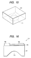
- Figs. 14 and 15 show a light-emitting element 100 having another type reflecting surface.
- the light-emitting element 100 has a sapphire substrate 101, a light-emitting layer 104, a p-electrode 108, and an n-electrode 109.
- a conical concave portion 111 is formed at substantially the center of the rear surface of the substrate 101 in the light-emitting element 100.
- the semiconductor layer structure of the light-emitting element 100 is substantially the same as that described above with reference to Fig. 1.
- the form for assembling the light-emitting element 100 is the same as the form shown in Fig. 4 or 5.
- a light component which is a part of light emitted from the light-emitting layer 104 and which advances toward the substrate 101 side, is reflected by the circumferential surface of the concave portion 111.
- the concave portion 111 is shaped like a cone here, the circumferential surface (i.e., the reflecting surface) of the concave portion 111 has line symmetry in all circumferential directions with respect to the center axis of the light-emitting element 100. Accordingly, the light is reflected from the center of the light-emitting element 100 in all circumferential directions, so that the light is emitted from side surfaces of the light-emitting element 100. As a result, light-emitting efficiency of the LED is improved.
- Fig. 16 shows an example of a light-emitting element 114 having a hemispherical concave portion 115.
- parts the same as those shown in Fig. 14 are denoted by the same reference numerals as those shown in Fig. 14 for the sake of omission of duplicated description.
- light can be emitted from side surfaces of the light-emitting element 114 in the same manner as the light-emitting element 100 shown in Fig. 14.
- a reflecting layer can be laminated on a surface of the concave portion 111 or 115 in the same manner as shown in Fig. 8.
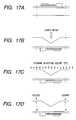
- Figs. 17A to 17D show a process for producing the light-emitting element 100 depicted in Fig. 14.
- step A the rear surface of the sapphire substrate 101 is polished by a known method to prepare the sapphire substrate 101 about 200 ⁇ m thick.
- step B the center of the element is decided on the basis of image recognition of the electrode pattern from the rear surface and the decided center (or its vicinity) is irradiated with a laser beam.
- the rear surface of the element is etched to form a concave portion.
- the third harmonic (355 nm) of a YAG pulse laser is used.
- a galvanometer mirror is used for scanning the rear surface of the element with this laser beam to thereby obtain a required concave shape.
- step C plasma or a blasting agent is applied on the whole region of the rear surface of the substrate 101 by a dry etching apparatus to thereby remove stains and molten layers caused by laser machining.
- step D a diamond scriber is used for scribing mark-off lines between chips. The wafer is pressed by a roller so as to be cut into chips.
Landscapes
- Led Devices (AREA)
- Led Device Packages (AREA)
Abstract
Description
| Layer | Composition |
| p-type layer 15 | p-GaN: |
| Layer | |
| 14 containing a light-emitting layer | including InGaN layer |
| n-type layer 13 | n-GaN: |
| Buffer layer | |
| 12 | |
| Substrate | |
| 11 | sapphire |
Claims (12)
- A Group III nitride compound semiconductor light-emitting element having a reflecting surface on a side opposite to a main light-emitting surface of said element viewed from a light-emitting layer thereof,
wherein said reflecting surface includes, as at least one portion, a surface inclined to a surface of growth of each semiconductor layer constituting the element, and said reflecting surface reflects light emitted from said light-emitting layer so that at least a part of the reflected light emerges from a side surface of said light-emitting element to the outside. - A Group III nitride compound semiconductor light-emitting element according to claim 1, wherein said reflecting surface is a rear surface of a substrate.
- A Group III nitride compound semiconductor light-emitting element according to claim 2, wherein a layer having a mirror surface is laminated on said rear surface of said substrate.
- A Group III nitride compound semiconductor light-emitting element according to claim 1, wherein said reflecting surface includes an irregular surface.
- A Group III nitride compound semiconductor light-emitting element according to claim 4, wherein said irregular surface is formed by blasting.
- A Group III nitride compound semiconductor light-emitting element according to claim 1, wherein said reflecting surface is a taper surface.
- A Group III nitride compound semiconductor light-emitting element according to claim 6; wherein said taper surface is formed by a dicer.
- A Group III nitride compound semiconductor light-emitting element according to claim 1, wherein said reflecting surface is a concave conical or hemispherical surface formed on a rear surface of a substrate.
- A Group III nitride compound semiconductor light-emitting element according to claim 8, wherein said reflecting surface is formed by laser machining.
- A Group III nitride compound semiconductor light-emitting element according to claim 1, wherein said light-emitting surface is on a substrate side whereas said reflecting surface is formed on a front surface of said semiconductor layer.
- A light-emitting device comprising a Group III nitride compound semiconductor light-emitting element according to any one of claims 1 through 10, and a side reflecting surface by which light emitted from the side surface of said light-emitting element is reflected toward an optical axis.
- A Group III nitride compound semiconductor light-emitting element having a reflecting surface on a side opposite to a main light-emitting surface of said element viewed from a light-emitting layer thereof,
wherein at least one portion of the reflecting surface is inclined with respect to a traveling direction of light emitted from the light-emitting layer, and said reflecting surface reflects the light emitted from said light-emitting layer so that at least a part of the reflected light emerges from a side surface of said light-emitting element to the outside.
Applications Claiming Priority (4)
| Application Number | Priority Date | Filing Date | Title |
|---|---|---|---|
| JP2002159613 | 2002-05-31 | ||
| JP2002159613 | 2002-05-31 | ||
| JP2003081901A JP2004056088A (en) | 2002-05-31 | 2003-03-25 | Group III nitride compound semiconductor light emitting device |
| JP2003081901 | 2003-03-25 |
Publications (2)
| Publication Number | Publication Date |
|---|---|
| EP1367656A2 true EP1367656A2 (en) | 2003-12-03 |
| EP1367656A3 EP1367656A3 (en) | 2005-04-13 |
Family
ID=29422471
Family Applications (1)
| Application Number | Title | Priority Date | Filing Date |
|---|---|---|---|
| EP03012365A Withdrawn EP1367656A3 (en) | 2002-05-31 | 2003-05-30 | Group III nitride compound semiconductor light-emitting element |
Country Status (3)
| Country | Link |
|---|---|
| US (1) | US6956245B2 (en) |
| EP (1) | EP1367656A3 (en) |
| JP (1) | JP2004056088A (en) |
Cited By (4)
| Publication number | Priority date | Publication date | Assignee | Title |
|---|---|---|---|---|
| WO2012010519A1 (en) * | 2010-07-23 | 2012-01-26 | Osram Opto Semiconductors Gmbh | Radiation-emitting component and method for producing radiation-emitting components |
| US8476644B2 (en) | 2007-04-26 | 2013-07-02 | Osram Opto Semiconductors Gmbh | Optoelectronic component and method for the manufacture of a plurality of optoelectronic components |
| WO2014108821A1 (en) * | 2013-01-10 | 2014-07-17 | Koninklijke Philips N.V. | Led with shaped growth substrate for side emission |
| WO2015118419A1 (en) * | 2014-02-06 | 2015-08-13 | Koninklijke Philips N.V. | Light emitting diode with structured substrate |
Families Citing this family (39)
| Publication number | Priority date | Publication date | Assignee | Title |
|---|---|---|---|---|
| US7304325B2 (en) * | 2000-05-01 | 2007-12-04 | Toyoda Gosei Co., Ltd. | Group III nitride compound semiconductor light-emitting device |
| JP2005019608A (en) * | 2003-06-25 | 2005-01-20 | Matsushita Electric Works Ltd | Semiconductor light emitting device |
| JP4593890B2 (en) * | 2003-07-28 | 2010-12-08 | 京セラ株式会社 | Manufacturing method of semiconductor light emitting device |
| TW200531310A (en) * | 2004-03-12 | 2005-09-16 | Opto Tech Corp | Light emitting diode with micro-lens layer |
| KR100568297B1 (en) * | 2004-03-30 | 2006-04-05 | 삼성전기주식회사 | Nitride semiconductor light emitting device and its manufacturing method |
| CN101587932B (en) | 2004-03-31 | 2011-06-01 | 日亚化学工业株式会社 | Nitride semiconductor light emitting element |
| JP4836410B2 (en) * | 2004-04-07 | 2011-12-14 | シャープ株式会社 | Nitride semiconductor light emitting device and manufacturing method thereof |
| JP2005347637A (en) * | 2004-06-04 | 2005-12-15 | Shurai Kagi Kofun Yugenkoshi | Light emitting device having increased luminous efficiency |
| JP4812369B2 (en) * | 2004-08-27 | 2011-11-09 | 京セラ株式会社 | Method for manufacturing light emitting device |
| KR101115532B1 (en) * | 2004-12-27 | 2012-03-08 | 서울옵토디바이스주식회사 | Luminescence device and method of manufacturing the same |
| JP2006253298A (en) * | 2005-03-09 | 2006-09-21 | Toshiba Corp | Semiconductor light emitting device and semiconductor light emitting device |
| JP4244953B2 (en) | 2005-04-26 | 2009-03-25 | 住友電気工業株式会社 | Light emitting device and manufacturing method thereof |
| JP2006344925A (en) * | 2005-05-11 | 2006-12-21 | Sharp Corp | Light emitting element mounting frame and light emitting device |
| JP2006324324A (en) | 2005-05-17 | 2006-11-30 | Sumitomo Electric Ind Ltd | Light emitting device, method for manufacturing light emitting device, and nitride semiconductor substrate |
| US7772604B2 (en) | 2006-01-05 | 2010-08-10 | Illumitex | Separate optical device for directing light from an LED |
| EP1995794A4 (en) * | 2006-03-10 | 2011-08-31 | Panasonic Elec Works Co Ltd | LIGHT EMITTING DEVICE |
| JP4282693B2 (en) | 2006-07-04 | 2009-06-24 | 株式会社東芝 | Semiconductor light emitting device and manufacturing method thereof |
| WO2008042351A2 (en) | 2006-10-02 | 2008-04-10 | Illumitex, Inc. | Led system and method |
| JP2008181910A (en) * | 2007-01-23 | 2008-08-07 | Mitsubishi Chemicals Corp | GaN-based light emitting diode device manufacturing method |
| KR100850667B1 (en) * | 2007-05-22 | 2008-08-07 | 서울옵토디바이스주식회사 | Light emitting diodes and manufacturing method |
| US7967476B2 (en) * | 2007-07-04 | 2011-06-28 | Nichia Corporation | Light emitting device including protective glass film |
| US8415695B2 (en) * | 2007-10-24 | 2013-04-09 | Switch Bulb Company, Inc. | Diffuser for LED light sources |
| JP2011512037A (en) | 2008-02-08 | 2011-04-14 | イルミテックス, インコーポレイテッド | System and method for emitter layer shaping |
| JP5227613B2 (en) * | 2008-02-27 | 2013-07-03 | スタンレー電気株式会社 | Semiconductor light emitting device |
| KR101047718B1 (en) * | 2008-11-26 | 2011-07-08 | 엘지이노텍 주식회사 | Light emitting element |
| TW201034256A (en) | 2008-12-11 | 2010-09-16 | Illumitex Inc | Systems and methods for packaging light-emitting diode devices |
| US7892869B2 (en) * | 2009-07-23 | 2011-02-22 | Edison Opto Corporation | Method for manufacturing light emitting diode assembly |
| US8585253B2 (en) | 2009-08-20 | 2013-11-19 | Illumitex, Inc. | System and method for color mixing lens array |
| US8449128B2 (en) | 2009-08-20 | 2013-05-28 | Illumitex, Inc. | System and method for a lens and phosphor layer |
| TWM382505U (en) * | 2010-01-15 | 2010-06-11 | Cheng Uei Prec Ind Co Ltd | Video device |
| KR101735670B1 (en) * | 2010-07-13 | 2017-05-15 | 엘지이노텍 주식회사 | A light emitting device |
| US9070851B2 (en) | 2010-09-24 | 2015-06-30 | Seoul Semiconductor Co., Ltd. | Wafer-level light emitting diode package and method of fabricating the same |
| KR20120100193A (en) * | 2011-03-03 | 2012-09-12 | 서울옵토디바이스주식회사 | Light emitting diode chip |
| US9263636B2 (en) * | 2011-05-04 | 2016-02-16 | Cree, Inc. | Light-emitting diode (LED) for achieving an asymmetric light output |
| JP5559108B2 (en) | 2011-08-05 | 2014-07-23 | 株式会社東芝 | Semiconductor light emitting device |
| JP2015072751A (en) * | 2013-10-01 | 2015-04-16 | 株式会社ジャパンディスプレイ | Organic EL display device |
| KR20150121306A (en) * | 2014-04-18 | 2015-10-29 | 포항공과대학교 산학협력단 | Nitride semiconductor light emitting device and producing method of the same |
| CN205944139U (en) | 2016-03-30 | 2017-02-08 | 首尔伟傲世有限公司 | Ultraviolet ray light -emitting diode spare and contain this emitting diode module |
| US11430919B2 (en) * | 2019-04-26 | 2022-08-30 | Lumileds Llc | High brightness LEDs with non-specular nanostructured thin film reflectors |
Family Cites Families (29)
| Publication number | Priority date | Publication date | Assignee | Title |
|---|---|---|---|---|
| JPS61110476A (en) * | 1984-11-02 | 1986-05-28 | Nec Corp | Infrared light emitting diode |
| EP0405757A3 (en) * | 1989-06-27 | 1991-01-30 | Hewlett-Packard Company | High efficiency light-emitting diode |
| JPH03227078A (en) * | 1990-01-31 | 1991-10-08 | Nec Corp | Light emitting diode |
| JPH06120560A (en) * | 1992-10-07 | 1994-04-28 | Victor Co Of Japan Ltd | Semiconductor light emitting device |
| JPH0722648A (en) * | 1993-07-06 | 1995-01-24 | Sanyo Electric Co Ltd | Silicon carbide light emitting diode device |
| JPH07183575A (en) * | 1993-12-24 | 1995-07-21 | Hitachi Cable Ltd | Compound semiconductor light emitting device and manufacturing method thereof |
| JP3326545B2 (en) * | 1994-09-30 | 2002-09-24 | ローム株式会社 | Semiconductor light emitting device |
| JPH0936427A (en) * | 1995-07-18 | 1997-02-07 | Showa Denko Kk | Semiconductor device and manufacturing method thereof |
| JPH0964421A (en) * | 1995-08-25 | 1997-03-07 | Nichia Chem Ind Ltd | Nitride semiconductor light emitting diode |
| US5779924A (en) * | 1996-03-22 | 1998-07-14 | Hewlett-Packard Company | Ordered interface texturing for a light emitting device |
| US6333522B1 (en) * | 1997-01-31 | 2001-12-25 | Matsushita Electric Industrial Co., Ltd. | Light-emitting element, semiconductor light-emitting device, and manufacturing methods therefor |
| JP3439063B2 (en) * | 1997-03-24 | 2003-08-25 | 三洋電機株式会社 | Semiconductor light emitting device and light emitting lamp |
| JPH11126925A (en) | 1997-10-21 | 1999-05-11 | Toyoda Gosei Co Ltd | Gallium nitride compound semiconductor light-emitting element |
| JPH11220168A (en) | 1998-02-02 | 1999-08-10 | Toyoda Gosei Co Ltd | Gallium nitride compound semiconductor device and manufacture thereof |
| JPH11220171A (en) | 1998-02-02 | 1999-08-10 | Toyoda Gosei Co Ltd | Gallium nitride compound semiconductor device |
| JP3847477B2 (en) | 1998-12-17 | 2006-11-22 | 豊田合成株式会社 | Group III nitride compound semiconductor light emitting device |
| JP3736181B2 (en) | 1998-05-13 | 2006-01-18 | 豊田合成株式会社 | Group III nitride compound semiconductor light emitting device |
| JP2000188421A (en) | 1998-12-21 | 2000-07-04 | Toyoda Gosei Co Ltd | Iii-group nitride-based compound semiconductor element |
| JP2000286445A (en) * | 1999-03-31 | 2000-10-13 | Toyoda Gosei Co Ltd | Group III nitride compound semiconductor light emitting device |
| US6531719B2 (en) * | 1999-09-29 | 2003-03-11 | Toyoda Gosei Co., Ltd. | Group III nitride compound semiconductor device |
| CN1292493C (en) * | 1999-12-03 | 2006-12-27 | 美商克立股份有限公司 | Enhanced light extration in LEDs through the use of internal and external optical elements |
| US6514782B1 (en) | 1999-12-22 | 2003-02-04 | Lumileds Lighting, U.S., Llc | Method of making a III-nitride light-emitting device with increased light generating capability |
| WO2001061765A1 (en) * | 2000-02-15 | 2001-08-23 | Osram Opto Semiconductors Gmbh | Semiconductor component which emits radiation, and method for producing the same |
| JP3864670B2 (en) * | 2000-05-23 | 2007-01-10 | 豊田合成株式会社 | Method for manufacturing group III nitride compound semiconductor light emitting device |
| JP2002261333A (en) * | 2001-03-05 | 2002-09-13 | Toyoda Gosei Co Ltd | Light emitting device |
| DE10111501B4 (en) * | 2001-03-09 | 2019-03-21 | Osram Opto Semiconductors Gmbh | Radiation-emitting semiconductor component and method for its production |
| JP3767420B2 (en) * | 2001-05-29 | 2006-04-19 | 豊田合成株式会社 | Light emitting element |
| JP4046485B2 (en) * | 2001-06-05 | 2008-02-13 | シャープ株式会社 | Nitride compound semiconductor light emitting device |
| JP2002374007A (en) * | 2001-06-15 | 2002-12-26 | Toyoda Gosei Co Ltd | Light emitting device |
-
2003
- 2003-03-25 JP JP2003081901A patent/JP2004056088A/en not_active Withdrawn
- 2003-05-30 EP EP03012365A patent/EP1367656A3/en not_active Withdrawn
- 2003-05-30 US US10/448,025 patent/US6956245B2/en not_active Expired - Fee Related
Cited By (8)
| Publication number | Priority date | Publication date | Assignee | Title |
|---|---|---|---|---|
| US8476644B2 (en) | 2007-04-26 | 2013-07-02 | Osram Opto Semiconductors Gmbh | Optoelectronic component and method for the manufacture of a plurality of optoelectronic components |
| CN101720513B (en) * | 2007-04-26 | 2013-10-30 | 欧司朗光电半导体有限公司 | Optoelectronic component and method for producing plurality of optoelectronic components |
| WO2012010519A1 (en) * | 2010-07-23 | 2012-01-26 | Osram Opto Semiconductors Gmbh | Radiation-emitting component and method for producing radiation-emitting components |
| US9159889B2 (en) | 2010-07-23 | 2015-10-13 | Osram Opto Semiconductors Gmbh | Radiation-emitting component and method for producing radiation-emitting components |
| WO2014108821A1 (en) * | 2013-01-10 | 2014-07-17 | Koninklijke Philips N.V. | Led with shaped growth substrate for side emission |
| CN104885235A (en) * | 2013-01-10 | 2015-09-02 | 皇家飞利浦有限公司 | LED with shaped growth substrate for side emission |
| WO2015118419A1 (en) * | 2014-02-06 | 2015-08-13 | Koninklijke Philips N.V. | Light emitting diode with structured substrate |
| US9941444B2 (en) | 2014-02-06 | 2018-04-10 | Koninklijke Philips N.V. | Light emitting diode with structured substrate |
Also Published As
| Publication number | Publication date |
|---|---|
| US6956245B2 (en) | 2005-10-18 |
| US20030222259A1 (en) | 2003-12-04 |
| JP2004056088A (en) | 2004-02-19 |
| EP1367656A3 (en) | 2005-04-13 |
Similar Documents
| Publication | Publication Date | Title |
|---|---|---|
| US6956245B2 (en) | Group III nitride compound semiconductor light-emitting element | |
| US7157294B2 (en) | Group III nitride compound semiconductor light-emitting element | |
| EP1471583B1 (en) | Nitride semiconductor device having support substrate and its manufacturing method | |
| JP5000612B2 (en) | Gallium nitride light emitting diode | |
| US7071495B2 (en) | III group nitride system compound semiconductor light emitting element and method of making same | |
| KR101208871B1 (en) | Light emitting devices having a reflective bond pad and methods of fabricating light emitting devices having reflective bond pads | |
| US6917059B2 (en) | III group nitride system compound semiconductor light emitting element | |
| KR20080065666A (en) | Nitride semiconductor light emitting device and nitride semiconductor light emitting device manufacturing method | |
| KR100992497B1 (en) | Light emitting diodes and manufacturing method thereof | |
| JP4325160B2 (en) | Nitride semiconductor light emitting device | |
| US20220254962A1 (en) | Optical arrangements in cover structures for light emitting diode packages and related methods | |
| US11367810B2 (en) | Light-altering particle arrangements for light-emitting devices | |
| US12557443B2 (en) | Contact structures in light-emitting diode chips for reduced voiding of bonding metals | |
| TWI910452B (en) | Metallic layer for dimming light-emitting diode chips | |
| TWI867543B (en) | Passivation structures for light-emitting diode chips | |
| CN100395901C (en) | Light emitting diode and method for manufacturing the same | |
| US20240120452A1 (en) | Reflectors for support structures in light-emitting diode packages | |
| JP4947569B2 (en) | Semiconductor light emitting device and manufacturing method thereof | |
| EP4533554A1 (en) | Contact structures in light-emitting diode chips | |
| US20250338682A1 (en) | Landing pad structures for contacts in light-emitting diode chips and related methods | |
| US20230395760A1 (en) | Passivation structures for light-emitting diode chips | |
| US20250006712A1 (en) | Stacked led chips | |
| TW202612555A (en) | Metallic layer for dimming light-emitting diode chips |
Legal Events
| Date | Code | Title | Description |
|---|---|---|---|
| PUAI | Public reference made under article 153(3) epc to a published international application that has entered the european phase |
Free format text: ORIGINAL CODE: 0009012 |
|
| 17P | Request for examination filed |
Effective date: 20030530 |
|
| AK | Designated contracting states |
Kind code of ref document: A2 Designated state(s): AT BE BG CH CY CZ DE DK EE ES FI FR GB GR HU IE IT LI LU MC NL PT RO SE SI SK TR |
|
| AX | Request for extension of the european patent |
Extension state: AL LT LV MK |
|
| PUAL | Search report despatched |
Free format text: ORIGINAL CODE: 0009013 |
|
| AK | Designated contracting states |
Kind code of ref document: A3 Designated state(s): AT BE BG CH CY CZ DE DK EE ES FI FR GB GR HU IE IT LI LU MC NL PT RO SE SI SK TR |
|
| AX | Request for extension of the european patent |
Extension state: AL LT LV MK |
|
| AKX | Designation fees paid |
Designated state(s): DE FR GB |
|
| STAA | Information on the status of an ep patent application or granted ep patent |
Free format text: STATUS: THE APPLICATION IS DEEMED TO BE WITHDRAWN |
|
| 18D | Application deemed to be withdrawn |
Effective date: 20060109 |