EP1367621A1 - Plasma display panel and method for manufacture thereof - Google Patents
Plasma display panel and method for manufacture thereof Download PDFInfo
- Publication number
- EP1367621A1 EP1367621A1 EP02711307A EP02711307A EP1367621A1 EP 1367621 A1 EP1367621 A1 EP 1367621A1 EP 02711307 A EP02711307 A EP 02711307A EP 02711307 A EP02711307 A EP 02711307A EP 1367621 A1 EP1367621 A1 EP 1367621A1
- Authority
- EP
- European Patent Office
- Prior art keywords
- silver
- electrode
- compound
- plasma display
- display panel
- Prior art date
- Legal status (The legal status is an assumption and is not a legal conclusion. Google has not performed a legal analysis and makes no representation as to the accuracy of the status listed.)
- Withdrawn
Links
Images



Classifications
-
- H—ELECTRICITY
- H01—ELECTRIC ELEMENTS
- H01J—ELECTRIC DISCHARGE TUBES OR DISCHARGE LAMPS
- H01J9/00—Apparatus or processes specially adapted for the manufacture, installation, removal, maintenance of electric discharge tubes, discharge lamps, or parts thereof; Recovery of material from discharge tubes or lamps
- H01J9/02—Manufacture of electrodes or electrode systems
-
- H—ELECTRICITY
- H01—ELECTRIC ELEMENTS
- H01J—ELECTRIC DISCHARGE TUBES OR DISCHARGE LAMPS
- H01J11/00—Gas-filled discharge tubes with alternating current induction of the discharge, e.g. alternating current plasma display panels [AC-PDP]; Gas-filled discharge tubes without any main electrode inside the vessel; Gas-filled discharge tubes with at least one main electrode outside the vessel
- H01J11/10—AC-PDPs with at least one main electrode being out of contact with the plasma
- H01J11/12—AC-PDPs with at least one main electrode being out of contact with the plasma with main electrodes provided on both sides of the discharge space
-
- H—ELECTRICITY
- H01—ELECTRIC ELEMENTS
- H01J—ELECTRIC DISCHARGE TUBES OR DISCHARGE LAMPS
- H01J11/00—Gas-filled discharge tubes with alternating current induction of the discharge, e.g. alternating current plasma display panels [AC-PDP]; Gas-filled discharge tubes without any main electrode inside the vessel; Gas-filled discharge tubes with at least one main electrode outside the vessel
- H01J11/20—Constructional details
- H01J11/22—Electrodes, e.g. special shape, material or configuration
-
- H—ELECTRICITY
- H01—ELECTRIC ELEMENTS
- H01J—ELECTRIC DISCHARGE TUBES OR DISCHARGE LAMPS
- H01J11/00—Gas-filled discharge tubes with alternating current induction of the discharge, e.g. alternating current plasma display panels [AC-PDP]; Gas-filled discharge tubes without any main electrode inside the vessel; Gas-filled discharge tubes with at least one main electrode outside the vessel
- H01J11/20—Constructional details
- H01J11/22—Electrodes, e.g. special shape, material or configuration
- H01J11/24—Sustain electrodes or scan electrodes
-
- H—ELECTRICITY
- H01—ELECTRIC ELEMENTS
- H01J—ELECTRIC DISCHARGE TUBES OR DISCHARGE LAMPS
- H01J2211/00—Plasma display panels with alternate current induction of the discharge, e.g. AC-PDPs
- H01J2211/20—Constructional details
- H01J2211/22—Electrodes
- H01J2211/225—Material of electrodes
Definitions
- the present invention relates to plasma display panels used as display devices, particularly to plasma display panels comprising silver electrodes.
- FPDs Flat Panel Displays
- FPDs Liquid Crystal Displays
- PDPs Plasma Display Panels
- FEDs Field Emission Displays
- ELs Electro Luminescence Display
- PDPs have characteristics that the other devices do not have, such as being self-luminous, being capable of displaying fine images, and being suitable for large-scale screens, and thus expectations are rising for the use of PDPs as wall-mounted large-screen TV displays.
- a PDP light emitting cells of different colors are disposed in a matrix.
- the Japanese Unexamined Patent Application Publication No. 9-35628 discloses an AC surface-discharge-type PDP.
- This PDP has a structure as follows: A front glass substrate and a rear glass substrate are arranged in parallel with barrier ribs interposed therebetween. On the front glass substrate, pairs of display electrodes (scanning electrodes and sustaining electrodes) are disposed in parallel. These electrodes are covered with a dielectric layer. On the rear glass substrate, address electrodes are disposed so as to oppose and intersect the scanning electrodes at right angles.
- Phosphor layers of respective colors are formed in spaces divided by the barrier ribs between the front and rear substrates. A discharge gas is enclosed in the spaces. This is how the cells that emit red, green and blue light are formed.
- a driving circuit applying voltage to each electrode, a discharge is generated, and ultraviolet rays are emitted.
- the phosphor layers are excited with these ultraviolet rays to emit light, resulting image displays.
- glass plates manufactured with a sodium borosilicate-system glass material using the float method are typically used for the front glass substrate and the rear glass substrate.
- silver electrodes that are relatively inexpensive are often used, although Cr-Cu-Cr (chromium-copper-chromium) electrodes are also used sometimes.
- the silver electrodes are formed using the thick-film forming method.
- a silver paste made of silver particles, a glass frit, a resin, a solvent, and the like is appliedas a pattern using the screen-printing method.
- a film made of silver particles, a glass frit, a resin, and the like is applied using the lamination method and is patterned.
- the applied paste or the applied film is baked at the temperature of 500 degrees centigrade or higher in order to fuse the silver particles together for improving conductivity as well as to remove the resin.
- the dielectric layer is usually formed by (i) applying a paste made of powdered lead glass with a low melting point or the like and a resin, using the screen-printing method, the die coat method, the lamination method, or the like, and (ii) heating and baking the applied paste at a temperature of 500 degrees centigrade or higher.
- the PDPs comprising such silver electrodes as described above are known to have a problem that the glass substrates and the dielectric layer tend to turn yellow around the silver electrodes. This yellowing in the glass substrates and the dielectric layer causes deterioration of luminance of blue cells, or a decrease in the color temperature at times of displaying full-white images, and may result in deterioration of image quality of the PDPs. Thus, there are demands for PDPs in which the glass substrates and the dielectric layer are less likely to turn yellow.
- the present invention provides a PDP in which silver electrodes are disposed on the substrates, wherein the silver electrodes further comprise an element or a compound whose standard electrode potential is lower than that of silver.
- the PDP may have an arrangement wherein the silver electrodes further comprise an element or a compound thereof, the element having a higher ionization tendency than silver.
- the Encyclopedic Dictionary of Chemistry (published by Tokyo Kagaku Dozin) reads that "an equilibrium electrode potential at such a time when all the substances engaged in the electrode reaction of a simple electrode are in the standard state is referred to as the standard electrode potential".
- the cause of yellowing around the silver electrodes is that, when the silver electrodes and the dielectric layer are baked, the silver included in the silver electrodes diffuses to the surroundings in the forms of ions, and the ions are then reduced at the glass substrates and inside the dielectric layer so as to form Ag colloids.
- the silver electrodes include an element or a compound whose standard electrode potential is lower than that of silver, or an element or a compound thereof, the element having higher ionization tendency than silver; therefore such an element or such a compound serves to inhibit ionization of the silver, and thus, it is possible to inhibit generation and diffusion of silver ions at times of baking. As a result, generation of silver colloidal particles around the silver electrodes is also inhibited, and thus yellowing of the panel can be prevented.
- a substance that serves to inhibit ionization of silver such as "an element or a compound whose standard electrode potential is lower than that of silver” will be referred to as "a silver ionization inhibiting substance”.
- a silver ionization inhibiting substance is “an element or a compound thereof that forms an oxide having a stronger chemical bond than silver”. Accordingly, “silver ionization inhibiting substances” include “an element or a compound thereof that forms an oxide having a stronger chemical bond than silver.”
- examples of substances that are preferable as silver ionization inhibiting substances include elements such as Cr, Al, In, B, Ti, as well as Ni, Pb, Zr, Sn, Zn and Co, and compounds of each of these elements. It has been also learned that it is preferable that the silver electrodes include the element or the compound of at least 1wt% of the silver.
- a silver ionization inhibiting substance exists as a layer that covers the silver electrodes, because the substance serves to inhibit ionization of silver likewise.
- the present invention also provides a manufacturing method of a PDP in which silver electrodes are disposed on the substrates, wherein the electrode material that is used for forming the silver electrodes includes a silver ionization inhibiting substance mentioned above.
- the electrode material that is used for forming the silver electrodes includes a silver ionization inhibiting substance mentioned above.
- an arrangement can be made so that, after the silver electrodes are formed, a coating layer is formed with a silver ionization inhibiting substance, so as to cover the silver electrodes.
- Examples of methods of forming a coating layer with a silver ionization inhibiting substance include the vacuum evaporation method, the sputtering method, the plating method, the CVD method, and the sol-gel method.
- the silver-electrode-purpose paste used for forming the electrodes of the PDP includes a silver ionization inhibiting substance that is mentioned above.
- the present invention provides a transfer film to be used for forming electrodes of a plasma display panel, the transfer film including a silver electrode film material layer that is disposed on a supporting film, wherein the silver electrode film material layer includes a silver ionization inhibiting substance mentioned above.
- FIG. 1 is a perspective assembly drawing showing the structure of an AC surface-discharge type PDP 100 in the embodiments.
- a front panel 101 as a first substrate and a rear panel 111 as a second substrate are pasted together with a perimeter sealing member (not shown in the drawing).
- display electrodes 103 are disposed in stripes on a front glass substrate 102; and a dielectric glass layer 106 and a protective layer 107 made up of Magnesium Oxide (MgO) cover the display electrodes 103 from the top.
- MgO Magnesium Oxide
- the rear panel 111 is made up of a rear glass substrate 112 on which address electrodes 113, a dielectric glass layer 114, barrier ribs 115, and phosphor layers 116 (in colors of red, green, and blue are arranged in order) are provided.
- the space between the front glass substrate 102 and the rear glass substrate 112 is divided into sections by barrier ribs 115 and a discharge gas is enclosed therein.
- the display electrodes 103 are provided extending perpendicular to the barrier ribs 115.
- the address electrodes 113 are provided extending in parallel to the barrier ribs 115. At intersections where the display electrodes 103 and the address electrodes 113 oppose each other, cells that emit light in colors of red, green, and blue are formed.
- the PDP display device is structured with a driving circuit that is connected to the display electrodes 103 and the address electrodes 113 in the PDP 100.
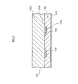
- FIG. 2 is a cross section of the front panel 101.
- a display electrode 103 is made up of (i) a silver electrode 105 that is narrower and includes silver, being provided on top of (ii) a transparent electrode 104 that is wider and made of transparent material.
- materials of which the transparent electrode 104 may be made include electrically conductive metal oxides such as ITO, SnO 2 , and ZnO.
- a display electrode 103 it is preferable to provide the silver electrode 105 on top of the transparent electrode 104 so as to maintain a large discharge area in a cell; however, it is also possible that a display electrode 103 is formed only with a silver electrode 105, without a transparent electrode 104.
- the silver electrodes 105 are made by baking a silver paste or a silver film which is for electrode-purpose and includes a silver ionization inhibiting substance.
- the silver electrodes 105 include silver particles and a glass frit, just like a normal silver electrode, and further include a silver ionization inhibiting substance, in addition, that serves to inhibit silver ionization.
- silver ionization inhibiting substances include those described in one of the following groups 1 ⁇ , 2 ⁇ , and 3 ⁇ .
- Examples of elements to be categorized in this group 1 ⁇ include: alkali metals (Li, Na, K, etc.); alkali-earth metals (Ca, Sr, Ba); Sc, Ti, V, Cr, Mn, Fe, Co, Ni, and Cu, which are transition metals (except for mercury) from which precious metals are excluded.
- alkali metals Li, Na, K, etc.
- alkali-earth metals Ca, Sr, Ba
- Sc Ti, V, Cr, Mn, Fe, Co, Ni, and Cu
- the limitation of excluding precious metals from transition metals is made because the standard electrode potential of a precious metal is generally higher than 0.8V.
- Examples of compounds to be categorized in this group 1 include an oxide, a hydroxide, a halide, a nitride, a carbide, a nitrate, a carbonate, and a sulfate of each of the elements above.
- silver ionization inhibiting substances are preferred as silver ionization inhibiting substances:
- Preferred elements are Ni, Pb, Zr, Sn, Zn, and Co, in addition to the elements described in the embodiments that will be mentioned later such as Cr, Al, In, B, and Ti.
- Preferred compounds are oxides of the aforementioned elements Cr, Al, In, B, Ti, Ni, Pb, Zr, Sn, Zn, and Co, i.e. ZrO 2 , SiO 2 , TiO 2 , Al 2 O 3 , B 2 O 3 , P 2 O 3 , In 2 O 3 and so on. (Each of these oxides has a stronger chemical bond than an oxide of silver.) Hydroxides and halides of the aforementioned elements Cr, Al, In, B, Ti, Ni, Pb, Zr, Sn, Zn, and Co are also preferable compounds.
- Nitrides such as TiN, ZnN, AlN, CrN, and BN as well as carbides such as TiC, SiC, and ZrC are also preferable compounds since each of them has a stronger chemical bond than an oxide of silver.
- the substances that are one of a nitrate, a carbonate, a sulfate, a hydroxide, and a halide are preferable because the valence of the metal element is maintained at the optimal level for inhibiting silver ionization at the time of baking electrodes.
- compounds such as Al(NO 3 ) 3 , Ca(NO 3 ) 2 , Zr(NO 3 ) 4 , Ni(NO 3 ) 2 , CO (NO 3 ) 2 , Pb(NO 3 ) 2 , BaCO 3 , NiCO 3 , MgCO 3 , ZnCO 3 , CoCO 3 and Cu 2 CO 3 are also preferable.
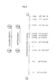
- FIG. 3 is a chart illustrating the relation among ionization tendency, electron energy, and standard electrode potential. The drawing shows the standard electrode potentials of some elements and ions.
- the lower the standard electrode potential is (the elements or compounds corresponding to the ions that are positioned in the upper side of the chart in FIG. 3), the larger the inhibitive influence on silver ionization is, and the larger the inhibitive influence on yellowing of the panel at the time of baking is.
- ions of an element have different standard electrode potentials depending on its valence. More specifically, it should be noted that, even if elements included in different compounds are the same kind, the standard electrode potentials of the compounds may vary depending on the valence of each of the elements included; therefore, a compound whose standard electrode potential is lower than silver, that is included in the silver electrodes 105, should be used as a silver ionization inhibiting substance.
- Chromium as an element
- Chromium Oxide Cr 2 O 3
- examples of preferable elements include Si, Al, and Ti
- examples of preferable compounds include SiO 2 , Al 2 O 3 , and TiO 2 .
- the silver particles in the silver electrodes when silver electrodes are exposed to the atmosphere, the silver particles in the silver electrodes get oxidized by the oxygen in the atmosphere into silver oxide, or get sulfurized by SO 2 in the atmosphere into silver sulfide. Also, when an oxide having a weaker chemical bond than an oxide of silver exists near the silver particles, the silver particles are easily exposed to the atmosphere, and tend to be turned into silver oxide. When turned into silver oxide, it tends to diffuse to the surroundings as silver ions.
- the silver electrodes include an element that forms an oxide having a stronger chemical bond than silver, or a compound of such an element, the element or the compound serves as a blockage to prevent the silver particles from being exposed to the atmosphere.
- the oxide of such an element has a stronger chemical bond than an oxide of silver, silver will not be turned into silver oxide by the oxide of such an element.
- the silver ionization inhibiting substance included in the silver electrodes is an element that forms an oxide having a stronger chemical bond than silver, or a compound of such an element, the silver included in the silver electrodes is even less likely to be ionized.
- the silver electrodes 105 include a silver ionization inhibiting substance that falls into one of the groups 1 ⁇ , 2 ⁇ , and 3 ⁇ , it is possible to inhibit ionization of silver at the time of baking.
- silver ionization inhibiting substances it is acceptable that only one kind of such an element or a compound is used; however, needless to say, it is also acceptable to use two or more kinds of them together after combining them or otherwise. Also, an alloy that includes two or more kinds of metal elements mentioned above is also considered as a silver ionization inhibiting substance.
- the ratio of a silver ionization inhibiting substance described in 1 ⁇ , 2 ⁇ , and 3 ⁇ to be included in the silver electrodes it is preferable to arrange it to be 0.1 wt% or larger of the silver in order to achieve effects of inhibiting the yellowing of the panel, and it is preferable to arrange it to be 0.5 wt% or larger of the silver in order to achieve sufficient effects. It is preferable to arrange it to be 1 wt% or larger of the silver in order to achieve more advantageous effects.
- the ratio of the element or the compound mentioned above is 20 wt% or smaller of the silver in order to ensure the conductivity of the silver electrodes, and it is further preferable to arrange it to be 10 wt% or smaller.
- the silver ionization inhibiting substance exists in such a state that it covers the silver particles, as will be explained later, and the effects of inhibiting silver ionization are therefore considered to be large.
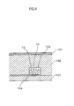
- FIG. 4 is a schematic cross section of the front panel 101 mentioned above, especially to schematically illustrate the internal structure of the silver electrodes 105.
- a plurality of silver particles 10 are bonded (in other words, silver particles 10 have fused with one another so as to form a conductive member); however, there are some spaces 11 between the silver particles 10. In these spaces 11, the glass frit and the silver ionization substance exist.
- the silver ionization inhibiting substance exists in the vicinity of thesurfaces of the silver particles 10 inside those spaces 11.
- silver is likely to be ionized, for example oxidized into silver oxide by the oxygen in the atmosphere, or sulfurized into silver sulfide by the SO 2 in the atmosphere, at the vicinity of the surfaces of the silver particles in the electrodes, while the silver electrodes are left in the atmosphere or while their temperature gets cooler after the baking.
- the silver ionization inhibiting substance in the spaces 11 exists in the vicinity of the surfaces of the silver particles, the silver ionization inhibiting substance is located at the right position where the silver tends to be in contact with the atmosphere and silver ions are more likely to be generated; we are therefore able have stronger effects of inhibiting silver ionization, while the silver electrodes are left in the atmosphere or while their temperature gets cooler after the baking.
- the diameter of a silver particle is approximately 1 ⁇ m to 3 ⁇ m. In view of this, it is preferable if the diameter of each of the particles in the silver ionization inhibiting substance to be used is 1 ⁇ m or smaller, so that it is easier for the silver ionization inhibiting substance to go into the spaces 11.
- the effects of inhibiting silver ionization as long as the silver ionization inhibiting substance is included in the vicinity of the surfaces of at least a part of the silver particles, not only when the silver ionization inhibiting substance exists in the vicinity of the surfaces of all the silver particles 10 inside the spaces 11; however, the effects of inhibiting silver ionization is strongest when it is arranged so that the silver ionization inhibiting substance exists in such a form that it covers the silver particles, and the silver ionization inhibiting substance exists on the surfaces of all the silver particles.
- the following explains the method of manufacturing the front panel 101, particularly, the process of forming the silver electrodes 105 and the dielectric glass layer 106.
- a glass plate manufactured using the float method is used as the front glass substrate 102.
- Transparent electrodes 104 are formed on the front glass substrate 102 using the normal thin-film forming method.
- the protective layer 107 is formed using the normal thin-film forming method. This is how the front panel 101 is manufactured.
- the following describes in detail how to form the silver electrodes 105 and the dielectric glass layer 106.
- Step 1 Forming a silver electrode precursor layer
- a silver electrode precursor layer which is a precursor of the silver electrodes 105 will be formed on the transparent electrodes 104, with either a silver paste or a silver electrode transfer film.
- a silver-electrode-purpose paste should be prepared.
- the paste includes, like the one used to form silver electrodes in general, silver powder, an organic binder, a glass frit (of PbO-B 2 O 3 -SiO 2 -system, ZnO-B 2 O 3 -SiO 2 -system, PbO-B 2 O 3 -SiO 2 -Al 2 O 3 -system, PbO-ZnO-B 2 O 3 -SiO 2 -system, Bi 2 O 3 -B 2 O 3 -SiO 2 -system etc.), an organic solvent, and the like.
- the amount of the silver ionization inhibiting substance to be mixed into the silver-electrode-purpose paste it is preferable to arrange it to be 0.1 wt% or larger of the silver powder, and it is preferable to arrange it to be 0.5 wt% or larger of the silver powder in order to achieve sufficient effects. It is preferable to arrange it to be 1 wt% or larger of the silver powder in order to achieve more advantageous effects. It is also preferable to arrange it to be 20wt% or smaller of the silver powder, and further preferable to arrange it to be 10 wt% or smaller.
- a cellulose compound such as ethyl cellulose or an acrylic polymer such as methyl methacrylate is preferable.
- a silver electrode transfer film is prepared by processing the same components as in the silver paste mentioned above into a film, and the film will be laminated on the transparent electrodes 104 in order to form the silver electrode precursor layer.
- the glass frit, the organic binder, and the silver ionization inhibiting substance exist around the silver particles.
- the silver ionization inhibiting substance to be mixed into the silver-electrode-purpose paste when the diameter of each of the particle is 1 ⁇ m or smaller, it is possible to densely cover the surfaces of the silver particles with the silver ionization inhibiting substance, and therefore possible to enhance the effects of inhibiting silver ionization.
- the following describes one of specific examples in which the silver electrode precursor layer is patterned using the photolithography method with use of a silver electrode transfer film, with reference to FIGs. 5A through 5D.
- FIG. 5A schematically illustrates the cross section of an electrode transfer film 200.
- a silver electrode precursor layer 202 and a cover film 203 are laminated on a supporting film 201.
- a silver-electrode-purpose paste in which silver powder, an organic binder made of a photosensitive resin, a glass frit, a silver ionization inhibiting substance, and an organic solvent are mixed together is applied to all over the supporting film 201 made of PET and dried, using a blade coater, so as to form the silver electrode precursor layer 202. Then, it is covered with the cover film 203 to which a mold releasing process has been applied.
- FIG. 5B shows how the silver electrode precursor layer 202 is laminated.
- the cover film 203 gets removed from the electrode transfer film 200, and the silver electrode precursor layer 202 gets superposed onto the front glass substrate 102 on which the transparent electrodes 104 have been formed, and gets pressed by a heating roller 210 from over the supporting film 201.
- the silver electrode precursor layer 202 gets pressed with heat onto the front glass substrate 102.
- the surface temperature of the heating roller 210 is 60 to 120 degrees centigrade, and the roller pressure is 1 to 5 kilograms/cm 2 , for example.
- FIG. 5C illustrates how the silver electrode precursor layer 202 is exposed to light.
- the supporting film 201 is removed, and the photomask 220 is superposed onto the silver electrode precursor layer 202.
- This photomask 220 has openings only at areas where the silver electrodes are to be formed. At times of light exposure, only those areas of the silver electrode precursor layer 202 where the silver electrodes are to be formed are exposed to light, and the photosensitive resin in the areas exposed to light gets hardened. Subsequently, when the silver electrode precursor layer 202 is developed, only the areas of the silver electrode precursor layer 202 that have been exposed to light remain, and thus are patterned in the shape of the silver electrodes 105.
- FIG. 5D shows the silver electrode precursor layer 202 that have been patterned.
- Step 2 Forming a dielectric precursor
- the electrode precursor layer that has been patterned in the process mentioned above will be covered by a dielectric precursor layer which is a precursor of the dielectric glass layer 106.
- the dielectric precursor layer by applying and drying a dielectric paste that includes glass and an organic binder as requisite components, as well as a solvent.
- Step 1 it is possible to form the dielectric precursor layer by pasting, using the lamination method, a dielectric sheet, which is in a form of film into which the requisite components of the dielectric paste are processed.
- Step 2 The outcome of Step 2 will be left, for minutes to tens of minutes, at a temperature that is the same as or higher than the softening point of the glass components included in the electrode precursor layer and the dielectric precursor layer.
- the silver electrode precursor layer and the dielectric precursor layer get baked at the same time .
- the silver electrode precursor layer changes into silver electrodes 105, and the dielectric precursor layer changes into dielectric glass layer 106.
- FIG. 7 describes the mechanism of the yellowing that occurs in the glass substrates and the dielectric glass layer of the PDP of the prior art.
- the substrate and the dielectric glass layer turn yellow.
- the silver ionization inhibiting substance serves to inhibit generation of silver ions, and it is therefore possible to inhibit generation of silver ions while the layer is left in the atmosphere or while its temperature gets cooler after the baking (Stage I above) .
- the silver ionization inhibiting substance serves to inhibit generation of silver ions, and it is therefore possible to inhibit generation of silver ions while the layer is left in the atmosphere or while its temperature gets cooler after the baking (Stage I above) .
- the PDP manufactured according to the method of the present embodiment has improved color temperature characteristics compared to a conventional PDP comprising silver electrodes.
- the silver electrode precursor layer and the dielectric precursor layer do not need to be baked at the same time. Instead, it is acceptable to form a silver electrode precursor layer in Step 1 and bake it, before performing Step 2 in which the dielectric precursor layer is formed; however, the effects of inhibiting the yellowing are expected to be stronger when the silver electrode precursor layer and the dielectric precursor layer are baked at the same time, because silver ions are less likely to diffuse on the glass substrate when the silver electrode precursor layer is baked while being covered by the dielectric precursor layer.
- the effects of inhibiting the yellowing of the panel can be achieved even with such a method by which the reduction of silver ions is inhibited after the silver ions diffuse to the substrates; however, the effects of inhibiting the yellowing of the panel are even stronger with the method of the present embodiment by which a silver ionization inhibiting substance is included in the silver electrodes, because generation of silver ions itself is inhibited at the source where the silver ions are generated.
- the dielectric glass layer will not be colored by the silver ionization inhibiting substance, because the silver ionization inhibiting substance is not added to the dielectric glass layer. Thus, it is easier to achieve a high color temperature at times of driving the PDP.
- the glass composition used in a dielectric glass layer is normally adjusted so that the softening temperature and the thermal expansion ratio are appropriate for the baking temperature of the dielectric glass layer in order to have less possibilities of having cracks at times of baking.
- cerium or the like is added to the glass to be used in a dielectric glass layer whose composition has already been adjusted, the softening temperature and the thermal expansion rate will be altered; it would be therefore necessary to adjust the glass composition again to correct the softening temperature and the thermal expansion rate.
- the panel performance will not be immediately degraded by the silver electrodes, unlike the case of the dielectric glass layer. Accordingly, it is more practical to have an arrangement, as in the present embodiment, in which a silver ionization inhibiting substance is included in the silver electrodes.
- the PDP of the second embodiment has the similar structure to the PDP of the first embodiment, except that, in the second embodiment, a coating layer 108 made of a silver ionization inhibiting substance is formed on the surfaces of the silver electrodes 105, as shown in FIG. 6, whereas the silver ionization inhibiting substance exists in the silver electrodes 105 on the front panel 101 in the first embodiment.
- examples of a silver ionization inhibiting substance of which the coating layer 108 is made include: alkali metals (Li, Na, K, etc.); alkali-earth metals (Ca, Sr, Ba); Sc, Ti, V, Cr, Mn, Fe, Co, Ni, and Cu, which are transition metals (except for mercury and manganese) from which precious metals are excluded; an oxide, a hydroxide, a halide, a nitride, a carbide, a nitrate, a carbonate, and a sulfate of the elements above.
- Preferred elements are Cr, Al, In, B, Ti, Ni, Pb, Zr, Sn, Zn, and Co.
- Preferred compounds are an oxide, a hydroxide, and a halide of the elements above.
- Nitrides such as TiN, ZnN, AlN, CrN, and BN as well as carbides such as TiC, SiC, and ZrC are also preferable compounds since each of them has a stronger chemical bond than an oxide of silver.
- the silver ionization inhibiting substance is used as an ingredient to make the coating layer by which the surfaces of the electrodes are covered; it is therefore preferable to use a metal element or, as to compounds, an oxide, a nitride, or a carbide, in view of easiness in forming the layer.
- the PDP of the present embodiment it is also possible to inhibit generation of silver ions on the silver electrodes 105 at the time of baking, like in the first embodiment, because of the silver ionization inhibiting substance included in the coating layer 108.
- the coating layer 108 it is preferable to form the coating layer 108 only on the surfaces of the silver electrodes 105 in order to ensure visible light transmittance of the front panel 101; however, when a non-conductive material with high transparency is used as a silver ionization inhibiting substance, it is possible to ensure visible light transmittance of the front panel 101 even if the coating layer 108 is formed on all over the surface of the glass substrate 102.
- the thickness of the coating layer 108 is 0.01 ⁇ m or more.
- the coating layer 108 is thicker, it would take more time and cost more to form the coating layer 108, besides there may be a possibility of causing a dielectric breakdown in the dielectric glass layer; therefore, it is preferable to arrange the thickness to be 1 ⁇ m or less.
- the manufacturing method of the front panel 101 of the second embodiment is similar to the manufacturing method of the front panel 101 of the first embodiment, except that there are differences in the process of forming the silver electrodes and the dielectric glass layer.
- the following describes the process of forming the silver electrodes and the dielectric glass layer.
- Step 1 Forming a silver electrode precursor layer
- This step is performed in the similar manner as Step 1 of the first embodiment, except that a silver ionization inhibiting substance does not get mixed in when the silver-electrode-purpose paste is prepared.
- Step 2 Baking the electrode precursor layer
- Step 1 The outcome of Step 1 will be left, for minutes to tens of minutes, at a temperature that is the same as or higher than the softening point of the glass components included in the silver electrode precursor, and then will cool down. Through this baking, the silver electrode precursor layer changes into the silver electrodes 105.
- a coating layer that is made of the aforementioned silver ionization inhibiting substance is formed so as to cover the silver electrodes 105 that have been formed.
- Examples of methods that can be used in forming such a coating layer includes: the vacuum evaporation method, the sputtering method, the plating method (the electroplating method, or the electroless plating method) , the sol-gel method, the ion plating method, and the CVD method.
- the coating process can be performed using a covering mask that has openings at areas where the silver electrodes 105 are positioned.
- the vacuum evaporation method is generally suitable for forming a coating layer made of a metal element or an alloy.
- a coating layer made of Al, Ni, Cr, Pb, Sn, Zr, B, or Ni-Cr alloy it is possible to form a coating layer made of an oxide, such as Al 2 O 3 , In 2 O 3 , or SiO 2 .
- the sputtering method it is possible to form a same kind of coating layer as when the vacuum evaporation method is used.
- the plating method is suitable for forming a coating layer made of a metal element, for example, made of Al, Ni, Cr, Pb, Sn, or Zr.
- the sol-gel method is suitable for forming a coating layer made of an oxide, e.g. ZrO 2 , SiO 2 , TiO 2 , AlO 2 , B 2 O 2 , or P 2 O 2 .
- an oxide e.g. ZrO 2 , SiO 2 , TiO 2 , AlO 2 , B 2 O 2 , or P 2 O 2 .
- the ion plating method and the CVD method are suitable for forming a coating layer made of an oxide, a nitride, or a carbide.
- a coating layer made of TiO 2 , ZnO 2 , AlO 2 , CrO 2 , TiN, ZnN, AlN, or CrN for instance.
- a coating layer made of B 2 O 3 , BN, or P 3 N 5 in addition to a coating layer made of an oxide or a nitride mentioned above .
- the layer is formed mainly on the top surfaces of the electrodes, and the layer is less likely to be formed on the side surfaces of the electrodes.
- a coating layer is formed using the electroplating method, however, it is possible to form the coating layer not only on the top surfaces of the silver electrodes, but also on the side surfaces of them.
- Step 4 Forming a dielectric precursor layer
- a dielectric precursor layer is formed so as to cover the silver electrodes that have been covered with the coating layer. This step is the same as Step 2 of the first embodiment.
- Step 4 is the same as Step 3 of the first embodiment, and the outcome of Step 4 will be baked at a temperature'that is the same as or higher than the softening point of the glass components included in the dielectric precursor layer.
- Step 5 baking process
- the silver electrodes are covered by the coating layer, and the silver ionization inhibiting substance included in the coating layer serves to inhibit generation of silver ions. Consequently, it is possible to inhibit generation of silver ions in the baking process.
- the silver electrodes are covered by the coating layer, it is possible to prevent the generated silver ions from diffusing.
- the PDP manufactured according to the aforementioned manufacturing method has improved color temperature characteristics compared to a conventional PDP comprising silver electrodes.
- the PDPs shown with the sampling numbers No. 1 through No. 5 each comprise silver electrodes that include Cr, Al, In, B, or Ti respectively as a silver ionization inhibiting substance according to the first embodiment. Those silver electrodes are made using different silver pastes to which each silver ionization inhibiting substance is added by 5 wt% of the silver particles.
- the PDPs shown with the sampling numbers No. 6 through No. 10 each comprise silver electrodes on the surfaces of which, according to the second embodiment, a coating layer made of a silver ionization inhibiting substance (Cr, Al, Al 2 O 3 , TiO 2 , or SiO 2 ) is formed using the vacuum evaporation method, within a range of thickness of 0.3 to 0.5 ⁇ m.
- a silver ionization inhibiting substance Cr, Al, Al 2 O 3 , TiO 2 , or SiO 2
- the PDP shown with the sampling number No. 11 is a comparison sample, and no silver ionization inhibiting substance is included in the silver electrodes, and no coating layer is formed.
- the glass substrates are "PD200" made by Asahi Glass Co., Ltd. using the float method.
- the dielectric glass layer is made with a dielectric glass paste whose main component is PbO-B 2 O 3 -SiO 2 -CaO-system glass, using the printing method so as to be approximately 30 ⁇ m in thickness.
- the MgO protective layer is made using the sputtering method.
- the cell size of PDP is arranged for a 42-inch VGA display, so that the height of the barrier ribs 115 is 0.15mm, the interval (the cell pitch) between the barrier ribs 115 is 0.36 mm, and the inter-electrode distance "d" between the display electrodes 103 is 0.10 mm.
- the "a*" value and the "b*" value were measured using a color-difference meter (Item No. NF777 manufactured by Nippon Denshoku Industries Co., Ltd.).
- the "a*" value and "b*" value are indicators of the coloring degree and the coloring tendency of the panels.
- the color temperature at the time of displaying the full-white image was measured using a multichannel spectrometer (MCPD-7000 manufactured by Otsuka Electronics Co., Ltd.).
- the PDP of No. 11 which is a comparison example, has the "b*" value of more than 10 and is presented with notable yellowing
- the PDPs of No. 1 through No. 10 according to the embodiments of the present invention each have the "b*" value in a range of 0.4 to 2.0 and is presented with hardly any yellowing.
- the color temperature is as low as 6400K, whereas in the PDPs of the embodiments, the color temperature is as high as 8900K or higher.
- the examples described are AC surface-discharge-type PDPs in which silver electrodes are covered by a dielectric glass layer; however, it is possible to achieve the same effects of inhibiting the yellowing of the glass substrates when the present invention is applied to a DC-type PDP in which silver electrodes are formed on the glass substrates so as to be exposed to the discharge space.
- the PDP and the PDP display device of the present invention are effective in use for display devices for computers and televisions, and particularly for large-scale display devices.
Landscapes
- Engineering & Computer Science (AREA)
- Physics & Mathematics (AREA)
- Plasma & Fusion (AREA)
- Manufacturing & Machinery (AREA)
- Chemical & Material Sciences (AREA)
- Materials Engineering (AREA)
- Gas-Filled Discharge Tubes (AREA)
Abstract
Description
| Sampling Number | Additive/ Covering Material | Additive Amount | Panel after baking the dielectric member | Panel Color Temperature | |
| Value a* | Value b* | ||||
| 1 | Cr | 5% | -1.2 | 0.8 | 9300 |
| 2 | Al | 5% | -1.8 | 1.5 | 9050 |
| 3 | In | 5% | -1.5 | 1.9 | 8930 |
| 4 | B | 5% | -2.5 | 2.0 | 8900 |
| 5 | Ti | 5% | -2.2 | 1.3 | 9080 |
| 6 | Cover with Cr | - | -1.5 | 0.4 | 9500 |
| 7 | Cover with Al | - | -1.8 | 0.9 | 9350 |
| 8 | Cover with Al2O3 | - | -1.3 | 0.8 | 9320 |
| 9 | Cover with TiO2 | - | -1.5 | 1.2 | 9040 |
| 10 | Cover with SiO2 | - | -1.4 | 1.1 | 9120 |
| *11 | None | None | -11.2 | 10.9 | 6400 |
| Sampling No. 11 is a comparison example |
Claims (29)
- A plasma display panel in which a pair of substrates are disposed opposing each other with a space therebetween, and an electrode including silver is disposed on at least one of the pair of substrates, wherein
the electrode further comprises an element or a compound whose standard electrode potential is lower than that of silver. - The plasma display panel of Claim 1, wherein
the silver included in the electrode is a plurality of silver particles bonded to one another, and
the element or the compound is positioned in a vicinity of surfaces of part or all of the silver particles. - The plasma display panel of Claim 1, wherein
the electrode comprises the element or the compound within a range of 1 wt% to 20 wt% inclusive of the silver. - A plasma display panel in which a pair of substrates are disposed opposing each other with a space therebetween, and an electrode including silver is disposed on at least one of the pair of substrates, wherein
the electrode further comprises an element or a compound whose standard electrode potential is lower than 0.8V. - A plasma display panel in which a pair of substrates are disposed opposing each other with a space therebetween, and an electrode including silver is disposed on at least one of the pair of substrates, wherein
the electrode further comprises an element or a compound thereof, the element having a higher ionization tendency than silver. - The plasma display panel of Claim 5, wherein
the element or the compound thereof forms an oxide that has a stronger chemical bond than silver. - A plasma display panel in which a pair of substrates are disposed opposing each other with a space therebetween, and an electrode including silver is disposed on at least one of the pair of substrates, wherein
the electrode comprises at least one element or one compound thereof, the element being selected from the group consisting of Cr, Al, In, Si, Ti, and B. - A plasma display panel in which a pair of substrates are disposed opposing each other with a space therebetween, and an electrode including silver is disposed on at least one of the pair of substrates, wherein
the electrode is covered with a layer that includes an element or a compound whose standard electrode potential is lower than that of silver. - A plasma display panel in which a pair of substrates are disposed opposing each other with a space therebetween, and an electrode including silver is disposed on at least one of the pair of substrates, wherein
the electrode is covered with a layer that includes an element or a compound thereof, the element having a higher ionization tendency than silver. - A plasma display panel of Claim 9, wherein
the element or the compound thereof forms an oxide that has a stronger chemical bond than silver. - A plasma display panel in which a pair of substrates are disposed opposing each other with a space therebetween, and an electrode including silver is disposed on at least one of the pair of substrates, wherein
the electrode is covered with a layer that includes at least one element or one compound thereof, the element being selected from the group consisting of Cr, Al, In, Si, Ti, and B. - A plasma display device comprising:a plasma display panel of any of Claims 1 to 11; anda driving circuit to drive the plasma display panel.
- A PDP manufacturing method comprising:whereina disposing step of disposing an electrode material including silver on a substrate; anda heating step of heating the electrode material disposed,
the electrode material further comprises an element or a compound whose standard electrode potential is lower than that of silver. - The PDP manufacturing method of Claim 13, wherein
the silver included in the electrode material is silver particles. - The PDP manufacturing method of Claim 13, wherein
the electrode material comprises the element or the compound within a range of 1 wt% to 20 wt% inclusive of the silver. - The PDP manufacturing method of Claim 13, wherein
in the heating step, the electrode material is heated up to a temperature at which the electrode material gets sintered. - A PDP manufacturing method comprising:a disposing step of disposing an electrode material including silver on a substrate; anda heating step of heating the electrode material disposed, whereinthe electrode material comprises an element or a compound thereof, the element having a higher ionization tendency than silver.
- The PDP manufacturing method of Claim 17, wherein
the element or the compound thereof forms an oxide that has a stronger chemical bond than silver. - A PDP manufacturing method comprising:a disposing step of disposing an electrode material including silver on a substrate;a heating step of heating the electrode material disposed; anda covering step, to be performed following the disposing step, of covering the electrode material with a layer that includes an element or a compound whose standard electrode potential is lower than that of silver.
- A PDP manufacturing method comprising:a disposing step of disposing an electrode material including silver on a substrate;a heating step of heating the electrode material disposed; anda covering step, to be performed following the disposing step, of covering the electrode material with a layer that includes an element or a compound thereof, the element having a higher ionization tendency than silver.
- The PDP manufacturing method of Claim 20, wherein
the element or the compound thereof forms an oxide that has a stronger chemical bond than silver. - A PDP manufacturing method comprising:a disposing step of disposing an electrode material including silver on a substrate; anda heating step of heating the electrode material disposed,
whereinthe electrode material further comprises at least one element or one compound thereof, the element being selected from the group consisting of Cr, Al, In, Si, Ti, and B. - A PDP manufacturing method comprising:a disposing step of disposing an electrode material including silver on a substrate;a heating step of heating the electrode material disposed; anda covering step, to be performed following the disposing step, of covering the electrode material with a layer that includes at least one element or one compound thereof, the element being selected from the group consisting of Cr, Al, In, Si, Ti, and B.
- A paste to be used for forming electrodes of a plasma display panel, the paste comprising:silver; andan element or a compound whose standard electrode potential is lower than that of silver.
- A paste to be used for forming electrodes of a plasma display panel, the paste comprising:silver; andan element or a compound thereof, the element having a higher ionization tendency than silver.
- A paste to be used for forming electrodes of a plasma display panel, the paste comprising:silver; andat least one element or one compound thereof, the element being selected from the group consisting of Cr, Al, In, Si, Ti, and B.
- A transfer film to be used for forming electrodes of a plasma display panel, the transfer film including an electrode film material layer that is disposed on a supporting film,
wherein
the electrode film material layer comprises:silver; andan element or a compound whose standard electrode potential is lower than that of silver. - A transfer film to be used for forming electrodes of a plasma display panel, the transfer film including an electrode film material layer that is disposed on a supporting film,
wherein
the electrode film material layer comprises:silver; andan element or a compound thereof, the element having a higher ionization tendency than silver. - A transfer film to be used for forming electrodes of a plasma display panel, the transfer film including an electrode film material layer that is disposed on a supporting film,
wherein
the electrode film material layer comprises:silver; andat least one element or one compound thereof, the element being selected from the group consisting of Cr, Al, In, Si, Ti, and B.
Applications Claiming Priority (3)
| Application Number | Priority Date | Filing Date | Title |
|---|---|---|---|
| JP2001029085 | 2001-02-06 | ||
| JP2001029085 | 2001-02-06 | ||
| PCT/JP2002/000912 WO2002063651A1 (en) | 2001-02-06 | 2002-02-05 | Plasma display panel and method for manufacture thereof |
Publications (2)
| Publication Number | Publication Date |
|---|---|
| EP1367621A1 true EP1367621A1 (en) | 2003-12-03 |
| EP1367621A4 EP1367621A4 (en) | 2008-10-29 |
Family
ID=18893470
Family Applications (1)
| Application Number | Title | Priority Date | Filing Date |
|---|---|---|---|
| EP02711307A Withdrawn EP1367621A4 (en) | 2001-02-06 | 2002-02-05 | PLASMA DISPLAY AND METHOD FOR MANUFACTURING THE SAME |
Country Status (6)
| Country | Link |
|---|---|
| US (1) | US7471042B2 (en) |
| EP (1) | EP1367621A4 (en) |
| KR (1) | KR100909735B1 (en) |
| CN (1) | CN1500282A (en) |
| TW (1) | TWI284345B (en) |
| WO (1) | WO2002063651A1 (en) |
Cited By (4)
| Publication number | Priority date | Publication date | Assignee | Title |
|---|---|---|---|---|
| EP1677333A1 (en) * | 2004-12-14 | 2006-07-05 | LG Electronics Inc. | Green sheet, plasma display panel and method for manufacturing plasma display panel |
| EP1517350A3 (en) * | 2003-09-18 | 2006-07-12 | Lg Electronics Inc. | Plasma display panel and method of manufacture |
| EP1763055A3 (en) * | 2005-09-12 | 2008-07-09 | Samsung SDI Co., Ltd. | Plasma Display Panel |
| EP1990821A4 (en) * | 2006-02-28 | 2010-04-28 | Panasonic Corp | PLASMA SCOREBOARD |
Family Cites Families (40)
| Publication number | Priority date | Publication date | Assignee | Title |
|---|---|---|---|---|
| US3803708A (en) * | 1973-02-16 | 1974-04-16 | Matsushita Electric Industrial Co Ltd | Method for making a resistor |
| JPS55107701A (en) * | 1979-02-14 | 1980-08-19 | Noritake Co Ltd | Palladium powder and production of palladium-powder-contained paste and palladium powder |
| US4541876A (en) * | 1983-10-31 | 1985-09-17 | Scm Corporation | Nonaqueous powdered metal paste composition |
| JPS63169006A (en) * | 1987-01-06 | 1988-07-13 | Murata Mfg Co Ltd | Chip type coil |
| GB8730196D0 (en) * | 1987-12-24 | 1988-02-03 | Johnson Matthey Plc | Silver-filled glass |
| JPH01274338A (en) | 1988-04-26 | 1989-11-02 | Noritake Co Ltd | Dc type electric discharge display tube and its manufacture |
| CA1334479C (en) * | 1988-08-29 | 1995-02-21 | Matsushita Electric Industrial Co., Ltd. | Conductive composition and method for making the same |
| US5339068A (en) * | 1992-12-18 | 1994-08-16 | Mitsubishi Materials Corp. | Conductive chip-type ceramic element and method of manufacture thereof |
| JPH07202063A (en) * | 1993-12-28 | 1995-08-04 | Toshiba Corp | Ceramics circuit board |
| AU3495595A (en) * | 1994-08-25 | 1996-03-22 | Qqc, Inc. | Nanoscale particles, and uses for same |
| JPH09190766A (en) * | 1995-11-08 | 1997-07-22 | Dainippon Printing Co Ltd | Method for manufacturing plasma display panel |
| US6156433A (en) * | 1996-01-26 | 2000-12-05 | Dai Nippon Printing Co., Ltd. | Electrode for plasma display panel and process for producing the same |
| JPH09231909A (en) | 1996-02-26 | 1997-09-05 | Daido Steel Co Ltd | Conductive paste compound for coloring electrode, and electrode |
| KR19980065367A (en) * | 1996-06-02 | 1998-10-15 | 오평희 | Backlight for LCD |
| JPH10100303A (en) * | 1996-06-07 | 1998-04-21 | Nippon Sheet Glass Co Ltd | Substrate fitted with transparent conductive film and display element using the same |
| JP3563236B2 (en) * | 1996-09-26 | 2004-09-08 | 触媒化成工業株式会社 | Coating liquid for forming transparent conductive film, substrate with transparent conductive film, method for producing the same, and display device |
| US5851732A (en) * | 1997-03-06 | 1998-12-22 | E. I. Du Pont De Nemours And Company | Plasma display panel device fabrication utilizing black electrode between substrate and conductor electrode |
| FR2760567B1 (en) * | 1997-03-06 | 1999-04-16 | Alsthom Cge Alcatel | POSITIVE ACTIVE MATERIAL FOR NICKEL ELECTRODE OF ALKALINE ELECTROLYTE BATTERY |
| JPH10302648A (en) | 1997-04-30 | 1998-11-13 | Asahi Glass Co Ltd | Glass substrate for plasma display |
| TW505685B (en) | 1997-09-05 | 2002-10-11 | Mitsubishi Materials Corp | Transparent conductive film and composition for forming same |
| JP3674261B2 (en) * | 1997-09-16 | 2005-07-20 | 東レ株式会社 | Plasma display |
| TWI231293B (en) * | 1997-11-12 | 2005-04-21 | Jsr Corp | Transfer film |
| JP3159250B2 (en) * | 1997-11-27 | 2001-04-23 | 日本電気株式会社 | Plasma display panel |
| JPH11242935A (en) | 1997-12-03 | 1999-09-07 | Sharp Corp | Plasma information display device |
| JPH11174993A (en) | 1997-12-10 | 1999-07-02 | Nippon Sheet Glass Co Ltd | Substrate with transparent conductive film and flat display device using the same |
| JPH11297210A (en) * | 1998-04-13 | 1999-10-29 | Mitsubishi Electric Corp | AC surface discharge type plasma display panel, method of manufacturing the same, and substrate for AC surface discharge type plasma display panel |
| EP1082433A4 (en) | 1998-05-29 | 2003-01-02 | Human Genome Sciences Inc | INTERLEUKINE 21 AND 22 |
| JP2000011892A (en) * | 1998-06-23 | 2000-01-14 | Hitachi Ltd | Gas discharge type display panel and display device using the same |
| KR100326535B1 (en) * | 1999-02-09 | 2002-03-25 | 구자홍 | Electrodes Of Plasma Display Panel And Fabrication Method Thereof |
| JP2000169764A (en) * | 1998-12-04 | 2000-06-20 | Jsr Corp | Glass paste composition, transfer film and method for producing plasma display panel |
| JP2000260336A (en) | 1999-01-06 | 2000-09-22 | Toray Ind Inc | Display substrate and method of manufacturing the same |
| JP4317288B2 (en) * | 1999-05-19 | 2009-08-19 | 大日本印刷株式会社 | Transfer sheet and pattern forming method |
| JP4158292B2 (en) * | 1999-09-09 | 2008-10-01 | Jsr株式会社 | Conductive resin composition and transfer film for electrode formation |
| US6444281B1 (en) * | 1999-10-13 | 2002-09-03 | Guardian Industries Corp. | Vacuum IG window unit with spacers between first and second edge seals |
| JP3299740B2 (en) | 1999-10-19 | 2002-07-08 | 松下電器産業株式会社 | How to make metal electrodes |
| CN1282981C (en) | 1999-10-19 | 2006-11-01 | 松下电器产业株式会社 | How to make a metal electrode |
| JP2001151532A (en) * | 1999-11-19 | 2001-06-05 | Asahi Glass Co Ltd | Low melting point glass for electrode coating and plasma display device |
| JP3389240B2 (en) | 1999-12-21 | 2003-03-24 | 松下電器産業株式会社 | Plasma display panel and method of manufacturing the same |
| EP1110647A3 (en) * | 1999-12-22 | 2004-02-11 | Mitsui Mining and Smelting Co., Ltd | Paste to be fired for forming circuit board and method for preparing surface-modified silver powder |
| JP2001236885A (en) | 2000-02-22 | 2001-08-31 | Matsushita Electric Ind Co Ltd | Plasma display panel and method of manufacturing the same |
-
2002
- 2002-02-05 CN CNA028072499A patent/CN1500282A/en active Pending
- 2002-02-05 EP EP02711307A patent/EP1367621A4/en not_active Withdrawn
- 2002-02-05 US US10/466,951 patent/US7471042B2/en not_active Expired - Fee Related
- 2002-02-05 WO PCT/JP2002/000912 patent/WO2002063651A1/en not_active Ceased
- 2002-02-05 TW TW091102011A patent/TWI284345B/en not_active IP Right Cessation
- 2002-02-05 KR KR1020037010302A patent/KR100909735B1/en not_active Expired - Fee Related
Cited By (7)
| Publication number | Priority date | Publication date | Assignee | Title |
|---|---|---|---|---|
| EP1517350A3 (en) * | 2003-09-18 | 2006-07-12 | Lg Electronics Inc. | Plasma display panel and method of manufacture |
| US7466079B2 (en) | 2003-09-18 | 2008-12-16 | Lg Electronics Inc. | Plasma display panel and method for manufacturing the same |
| EP1677333A1 (en) * | 2004-12-14 | 2006-07-05 | LG Electronics Inc. | Green sheet, plasma display panel and method for manufacturing plasma display panel |
| EP1763055A3 (en) * | 2005-09-12 | 2008-07-09 | Samsung SDI Co., Ltd. | Plasma Display Panel |
| US7462988B2 (en) | 2005-09-12 | 2008-12-09 | Samsung Sdi Co., Ltd. | Plasma display panel having a layer including carbon |
| EP1990821A4 (en) * | 2006-02-28 | 2010-04-28 | Panasonic Corp | PLASMA SCOREBOARD |
| US7990065B2 (en) | 2006-02-28 | 2011-08-02 | Panasonic Corporation | Plasma display panel with improved luminance |
Also Published As
| Publication number | Publication date |
|---|---|
| KR100909735B1 (en) | 2009-07-29 |
| EP1367621A4 (en) | 2008-10-29 |
| WO2002063651A1 (en) | 2002-08-15 |
| KR20030070152A (en) | 2003-08-27 |
| US20040080270A1 (en) | 2004-04-29 |
| TWI284345B (en) | 2007-07-21 |
| US7471042B2 (en) | 2008-12-30 |
| CN1500282A (en) | 2004-05-26 |
Similar Documents
| Publication | Publication Date | Title |
|---|---|---|
| US6777872B2 (en) | Plasma display panel and method for production thereof | |
| KR100338269B1 (en) | Color plasma display panel and method of manufacturing the same | |
| US20080238316A1 (en) | Plasma dispaly panel and manufacturing method of the same | |
| CN101326612B (en) | Plasma display panel | |
| US7471042B2 (en) | Plasma display panel with an improved electrode | |
| US20090026952A1 (en) | Phosphor paste and plasma display panel using the same | |
| CN1287407C (en) | Plasma display | |
| US7932675B2 (en) | Plasma display panel | |
| CN1545715A (en) | Method for manufacturing plasma display panel | |
| JPH11109888A (en) | Stacked electrode | |
| JP4300733B2 (en) | Display device | |
| JP2002313241A (en) | Plasma display panel and method of manufacturing the same | |
| US20100207922A1 (en) | Plasma display panel and method for manufacturing the same | |
| JP3846636B2 (en) | Plasma display panel and manufacturing method thereof | |
| JP4197190B2 (en) | Plasma display panel | |
| US7768205B2 (en) | Plasma display panel and method of manufacturing the same | |
| KR20090093453A (en) | Plasma display panel and method for fabricating the same | |
| JP2005135831A (en) | Plasma display panel | |
| JP2006032044A (en) | Plasma display panel | |
| US20110102399A1 (en) | Plasma display panel and method for manufacturing the same | |
| CN101414531A (en) | Plasma display panel and method for manufacturing same | |
| US20110221728A1 (en) | Plasma display panel and method for manufacturing the same | |
| JPH11339669A (en) | Plasma display substrate and method of manufacturing the same | |
| JPWO2008032355A1 (en) | Plasma display panel and phosphor layer forming method thereof | |
| KR20050096996A (en) | Plasma display panel and making method thereof |
Legal Events
| Date | Code | Title | Description |
|---|---|---|---|
| PUAI | Public reference made under article 153(3) epc to a published international application that has entered the european phase |
Free format text: ORIGINAL CODE: 0009012 |
|
| 17P | Request for examination filed |
Effective date: 20030905 |
|
| AK | Designated contracting states |
Kind code of ref document: A1 Designated state(s): AT BE CH CY DE DK ES FI FR GB GR IE IT LI LU MC NL PT SE TR |
|
| RIN1 | Information on inventor provided before grant (corrected) |
Inventor name: SUMIDA, KEISUKE Inventor name: FUJITANI, MORIO Inventor name: HIBINO, JUNICHI Inventor name: AOKI, MASAKI Inventor name: ADACHI, DAISUKE Inventor name: ASIDA, HIDEKI Inventor name: YONEHARA, HIROYUKI |
|
| A4 | Supplementary search report drawn up and despatched |
Effective date: 20080929 |
|
| RAP1 | Party data changed (applicant data changed or rights of an application transferred) |
Owner name: PANASONIC CORPORATION |
|
| 17Q | First examination report despatched |
Effective date: 20090525 |
|
| STAA | Information on the status of an ep patent application or granted ep patent |
Free format text: STATUS: THE APPLICATION IS DEEMED TO BE WITHDRAWN |
|
| 18D | Application deemed to be withdrawn |
Effective date: 20120901 |