EP1366552B1 - Semiconductor device with protective functions - Google Patents
Semiconductor device with protective functions Download PDFInfo
- Publication number
- EP1366552B1 EP1366552B1 EP01970240A EP01970240A EP1366552B1 EP 1366552 B1 EP1366552 B1 EP 1366552B1 EP 01970240 A EP01970240 A EP 01970240A EP 01970240 A EP01970240 A EP 01970240A EP 1366552 B1 EP1366552 B1 EP 1366552B1
- Authority
- EP
- European Patent Office
- Prior art keywords
- transistor
- mosfet
- electrode
- protective
- main
- Prior art date
- Legal status (The legal status is an assumption and is not a legal conclusion. Google has not performed a legal analysis and makes no representation as to the accuracy of the status listed.)
- Expired - Lifetime
Links
Images


Classifications
-
- H—ELECTRICITY
- H03—ELECTRONIC CIRCUITRY
- H03K—PULSE TECHNIQUE
- H03K17/00—Electronic switching or gating, i.e. not by contact-making and –breaking
- H03K17/08—Modifications for protecting switching circuit against overcurrent or overvoltage
-
- H—ELECTRICITY
- H03—ELECTRONIC CIRCUITRY
- H03K—PULSE TECHNIQUE
- H03K17/00—Electronic switching or gating, i.e. not by contact-making and –breaking
- H03K17/51—Electronic switching or gating, i.e. not by contact-making and –breaking characterised by the components used
- H03K17/78—Electronic switching or gating, i.e. not by contact-making and –breaking characterised by the components used using opto-electronic devices, i.e. light-emitting and photoelectric devices electrically- or optically-coupled
- H03K17/785—Electronic switching or gating, i.e. not by contact-making and –breaking characterised by the components used using opto-electronic devices, i.e. light-emitting and photoelectric devices electrically- or optically-coupled controlling field-effect transistor switches
-
- H—ELECTRICITY
- H03—ELECTRONIC CIRCUITRY
- H03K—PULSE TECHNIQUE
- H03K17/00—Electronic switching or gating, i.e. not by contact-making and –breaking
- H03K17/08—Modifications for protecting switching circuit against overcurrent or overvoltage
- H03K17/082—Modifications for protecting switching circuit against overcurrent or overvoltage by feedback from the output to the control circuit
- H03K17/0822—Modifications for protecting switching circuit against overcurrent or overvoltage by feedback from the output to the control circuit in field-effect transistor switches
-
- H—ELECTRICITY
- H10—SEMICONDUCTOR DEVICES; ELECTRIC SOLID-STATE DEVICES NOT OTHERWISE PROVIDED FOR
- H10D—INORGANIC ELECTRIC SEMICONDUCTOR DEVICES
- H10D89/00—Aspects of integrated devices not covered by groups H10D84/00 - H10D88/00
- H10D89/60—Integrated devices comprising arrangements for electrical or thermal protection, e.g. protection circuits against electrostatic discharge [ESD]
- H10D89/601—Integrated devices comprising arrangements for electrical or thermal protection, e.g. protection circuits against electrostatic discharge [ESD] for devices having insulated gate electrodes, e.g. for IGFETs or IGBTs
- H10D89/811—Integrated devices comprising arrangements for electrical or thermal protection, e.g. protection circuits against electrostatic discharge [ESD] for devices having insulated gate electrodes, e.g. for IGFETs or IGBTs using FETs as protective elements
-
- H—ELECTRICITY
- H03—ELECTRONIC CIRCUITRY
- H03K—PULSE TECHNIQUE
- H03K17/00—Electronic switching or gating, i.e. not by contact-making and –breaking
- H03K17/08—Modifications for protecting switching circuit against overcurrent or overvoltage
- H03K2017/0806—Modifications for protecting switching circuit against overcurrent or overvoltage against excessive temperature
Definitions
- the present invention relates to a semiconductor device with protective functions, which can operate with a very small gate driving current and further automatically dissolve its protective function when abnormality of a main transistor has run out.
- the semiconductor device shown in Fig. 11 is provided with a main MOSFET 1 which is turned to ON or OFF in accordance with the control voltage and which is inserted between the external drain terminal D and the external source terminal S, and a protective circuit 3' for protecting the main MOSFET 1.
- the protective circuit 3' is provided with a protective MOSFET 5' inserted between the gate electrode and the source electrode of the main MOSFET 1, a diode array 31 acting as a temperature detector which is thermally connected with the main MOSFET 1, another MOSFET 35 connected to the diode array 31 at each of the gate electrode and the source electrode thereof, further MOSFETs 37 and 38 connected to each other in such a manner that the drain electrode of the MOSFET 37 is connected to the gate electrode of the MOSFET 38, and a further MOSFET 36 inserted between the drain electrode and source electrode of the MOSFET 37, the gate electrode of the MOSFET 36 being connected to the drain electrode of the MOSFET 35.
- the main MOSFET 1 when the temperature detected by the diode array 31 rises to or over a predetermined value, the main MOSFET 1 is shut, and then the shut state of the main MOSFET 1 is maintained till the input to the external gate terminal G is reset. That is, when the temperature detected by the diode array 31 rises to or over the predetermined value, the gate voltage of the MOSFET 35 becomes lower than a threshold voltage. In consequence, the MOSFET 35 becomes OFF, the MOSFET 36 becomes ON, and each of the MOSFETs 37 and becomes OEF. As the result, the protective MOSFET 5' becomes ON so that the gate electrode and source electrode of the main MOSFET 1 short-circuit, and then the main MOSFET 1 becomes OFF.
- the main MOSFET 1 is shut.
- the shut state of the main MOSFET 1 is maintained till the input to the external gate terminal G is reset. Therefore, when the semiconductor device is restarted (returned), the control voltage applied to the external gate terminal G is required to be reset as 0 V.
- a power MOSFET according to US 4,893,158 is provided with a protective circuit including a monitor MOSFET whose drain is connected with the drain of the power MOSFET, a monitor resistor connected between the sources of the power and monitor MOSFETs, and a monitor transistor for decreasing a gate voltage of the power MOSFET when a voltage across the monitor resistor exceeds a predetermined level representing a dangerous condition of the device.
- the present invention which has been developed to solve the conventional problems described above, has an object to provide a semiconductor device, with protective functions which can operate with a very small gate driving current and further automatically dissolve its protective function (or protected state) when abnormality of a main transistor has run out. This object is solved by the features of claim 1.
- the semiconductor device through the first main terminal and the detecting transistor, the power is supplied from the power source to the protective circuit inserted between the first main terminal and the second main terminal, which protects the main transistor by the protective transistor when the abnormality is detected thereby. Accordingly, it is not necessary to supply the power from the driver to both of the protective circuit and the main transistor, as different from the conventional case. In consequence, the semiconductor device can operate with a very small gate driving current. Meanwhile, when the abnormality of the main transistor has run out, the protective function, which has protected the main transistor, is automatically dissolved.
- each of the transistors constituting the semiconductor device is not one of a current driven type such as a bipolar transistor, but one of a voltage driven type, the transistors can be formed on one single (same) substrate.
- the semiconductor device when the current flows from the second main terminal to the first main terminal, it may be prevented that the current flows into the protective circuit. In consequence, it may be prevented that the protective circuit operates in error.
- a semiconductor device with protective functions may have two semiconductor device components inserted between a power source and a load, in each of which an electric current flowing between a first main terminal and a second main terminal is controlled in accordance with a control voltage applied between a control terminal and the second main terminal, the second main terminals of the two semiconductor device components being commonly connected to each other, and the control terminals of the two semiconductor device components being commonly connected to each other.
- Each of the semiconductor device components is characterized in that it includes (i) a main transistor of a voltage driven type which is turned to ON or OFF in accordance with the control voltage, the main transistor being inserted between the first main terminal and the second main terminal, (ii) a protective transistor of a voltage driven type inserted between a control electrode of the main transistor and a reference electrode of the main transistor, (iii) a protective circuit which protects the main transistor by the protective transistor when abnormality is detected thereby, the protective circuit being inserted between the first main terminal and the second main terminal, (iv) a detecting transistor of a voltage driven type which is turned to ON or OFF in accordance with the control voltage, the detecting transistor being inserted between the first main terminal and the protective circuit, (v) an impedance element inserted between the protective transistor and a junction connecting the control terminal to a control electrode of the detecting transistor, and (vi) a non-return diode inserted between the second main terminal and a junction connecting the protective circuit to a reference electrode of the
- the semiconductor device when the two-directional switching is performed, it may be prevented that the protective circuit operates in error. Meanwhile, through the first main terminal and the detecting transistor, the power is supplied from the power source to the protective circuit inverted between the first main terminal and the second main terminal, which protects the main transistor by the protective transistor when the abnormality is detected thereby. Accordingly, it is not necessary to supply the power from the driver to both of the protective circuit and the main transistor, as different from the conventional case. In consequence, the semiconductor device can operate with a very small gate driving current. Meanwhile, when the abnormality of the main transistor, has run out, the protective function, which has protected the main transistor, is automatically dissolved.
- the device further includes (a) a light emitting element which is turned on or turned off in accordance with a signal inputted thereto, and (b) a photovoltaic element which is optically coupled with the light emitting element to generate electromotive force, wherein (c) the electromotive force is applied between the control terminal and the second main terminal.
- the input terminal and the output terminal may be insulated to each other.
- the input terminal and the output terminal may be insulated to each other for a direct current.
- thermosensible element with a negative temperature characteristic, which is composed of semiconductor
- thermosensible element being thermally connected with the main transistor
- a protective circuit transistor of a voltage driven type its one side electrode being connected to the control electrode of the protective transistor, its further side electrode being connected to one end portion of the thermosensible element and the further side electrode of the protective transistor, and its control electrode being connected to the other end portion of the thermosensible element
- the protective circuit transistor is inserted between the first main terminal and the second main terminal so as to be provided with a power through the detecting transistor, the control electrode of the protective circuit transistor being connected in such a manner that conductivity between its both side electrodes is shut in accordance with a potential rise between the first main terminal and the second main terminal.
- the detecting transistor is composed of two or more detecting transistor components, while (b) for each of the main transistor, the detecting transistor components and the protective transistor, conductivity between a one side electrode and a further side electrode acting as a reference electrode is actuated (driven) by a potential difference between the further side electrode and a control electrode, (c) the protective circuit including a thermosensible element with a negative temperature characteristic, which is composed of semiconductor, the thermosensible element being thermally connected with the main transistor, and a protective circuit transistor of a voltage driven type, its one side electrode being connected to the control electrode of the protective transistor, its further side electrode being connected to one end portion of the thermosensible element and the further side electrode of the protective transistor, and its control electrode being connected to the other end portion of the thermosensible element, wherein (d) the protective circuit transistor is inserted between the first main terminal and the second main terminal so as to be provided with a power through any one of the detecting transistor components, the control
- the semiconductor device further includes a non-return diode inserted between the second main terminal and the further electrode of each of the protective transistor and the protective circuit transistor, in such a manner that the non-return diode has polarity to prevent a current from flowing from the second main terminal to the protective transistor and the protective circuit.
- each of the main transistor, the detecting transistor components and the protective transistor may be composed of a MOSFET having a drain electrode as the one side electrode, a source electrode as the further side electrode and a gate electrode as the control electrode.
- each of the main transistor, the detecting transistor and the protective transistor is composed of a MOSFET
- the protective circuit includes second, third and fourth impedance elements, each of which is commonly connected to a source electrode of the detecting transistor at one end portion thereof, first, second and third MOSFETs, each of which is commonly connected to the second main terminal at a source electrode thereof, and a diode array which is thermally connected with the main transistor and inserted between a drain electrode of the second MOSFET and the source electrode of the second MOSFET in such a manner that an anode side of the diode array is connected to the drain electrode of the second MOSFET, wherein (c) a further end portion of the second impedance element is connected to a drain electrode of the first MOSFET, a further end portion of the third impedance element being connected to the drain electrode of the second MOSFET, a further end portion of the fourth impedance element being connected to a drain electrode of the third MOSF
- each of the impedance elements and each of diodes constituting the diode array are formed utilizing materials of the gate electrodes of the MOSFETs, the diode array, each of the impedance elements and each of the MOSFETs can be formed on one single substrate by means of a simple process.
- each of the main transistor, the detecting transistor and the protective transistor is composed of a MOSFET
- the protective circuit includes second, third and fourth impedance elements, each of which is commonly connected to a source electrode of the detecting transistor at one end portion thereof, first, second and third MOSFETs, each of which is commonly connected to an anode of the non-return diode at a source electrode thereof, and a diode array which is thermally connected with the main transistor and inserted between a drain electrode of the second MOSFET and a source electrode of the main transistor in such a manner that an anode side of the diode array is connected to the drain electrode of the second MOSFET, wherein (c) a further end portion of the second impedance element is connected to a drain electrode of the first MOSFET, a further end portion of the third impedance element being connected to the drain electrode of the second MOSFET, a further end portion of the fourth impedance element being connected to
- each of the impedance elements and each of diodes constituting the diode array are formed utilizing materials of the gate electrodes of the MOSFETs, these can be formed on one single substrate by means of a simple process.
- the detecting transistor is composed of a first detection transistor and a second detection transistor
- each of the main transistor, the first detection transistor, the second detection transistor and the protective transistor being composed of a MOSFET
- the impedance element being defined as a first impedance element
- the protective circuit including second and third impedance elements, each of which is commonly connected to a source electrode of the first detection transistor at one end portion thereof, first and second MOSFETs, each of which is commonly connected to a source electrode of the main transistor at a source electrode thereof, a diode array which is thermally connected with the main transistor and inserted between a drain electrode of the second MOSFET and the source electrode of the second MOSFET in such a manner that an anode side of the diode array is connected to the drain electrode of the second MOSFET, and a fourth impedance element which is connected to a source electrode of the second detection transistor at one end portion thereof and to the source electrode of the main transistor at
- the detecting transistor is composed of a first detection transistor and a second detection transistor
- each of the main transistor, the first detection transistor, the second detection transistor and the protective transistor being composed of a MOSFET
- the impedance element being defined as a first impedance element
- the protective circuit including second and third impedance elements, each of which is commonly connected to a source electrode of the first detection transistor at one end portion thereof, first and second MOSFETs, each of which is commonly connected to an anode of the non-return diode at a source electrode thereof, a diode array which is thermally connected with the main transistor and inserted between a drain electrode of the second MOSFET and a source electrode of the main transistor in such a manner that an anode side of the diode array is connected to the drain electrode of the second MOSFET, and a fourth impedance element which is connected to a source electrode of the second detection transistor at one end portion thereof and to the source electrode
- each of the impedance elements and each of diodes constituting the diode array are formed utilizing materials of the gate electrodes of the MOSFETs, these can be formed on one single substrate by means of a simple process.
- the main transistor, the detecting transistor, the protective transistor, the protective circuit and the impedance element are formed on one substrate.
- the size of the semiconductor device may be reduced in comparison with such a case that it is constructed by combining discrete parts.
- characteristics of the elements constituting the semiconductor device may be uniformed.
- each of the main transistor, the detecting transistor and the protective transistor is formed as a MOSFET, each of the impedance elements can be formed using polycrystalline silicon which is a material of the gate electrodes of the MOSFETs. In consequence, the process for manufacturing the semiconductor device may be simplified.
- each of diodes constituting the diode array can be formed using polycrystalline silicon, which is a material of the gate electrodes of the MOSFETs.
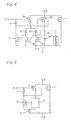
- the semiconductor device with protective functions according to Embodiment 1 which is one of three-terminal semiconductor devices, is provided with an external drain terminal D, an external source terminal S and an external gate terminal G.
- the semiconductor device is inserted between a power source and a load.
- a current flowing between the external drain terminal D and the external source terminal S is controlled in accordance with a control voltage applied between the external gate terminal G and the external source terminal S.
- the external drain terminal D composes the first main terminal, the external source terminal S composing the second main terminal, and the external gate terminal G composing the control terminal.
- the semiconductor device is provided with a main MOSFET 1, a detecting MOSFET 2, a protective circuit 3, a first impedance element 4 and a protective MOSFET 5.
- the main MOSFET 1 is inserted between the external drain terminal D and the external source terminal S while it is turned to ON or OFF (i.e. becomes ON or OFF) in accordance with the control voltage.
- the protective MOSFET 5 is inserted between the gate electrode (control electrode) and the source electrode (reference electrode) of the main MOSFET 1.
- the detecting MOSFET 2 which is inserted between the external drain terminal D and the protective circuit 3, is turned to ON or OFF (i.e. becomes ON or OFF) in accordance with the control voltage.
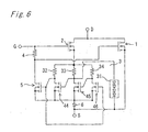
- Fig. 2 shows the circuit shown in Fig. 1 more concretely.
- the protective circuit 3 is provided with a diode array 31, second to fourth impedance elements 32-34 and first to third MOSFETs 44-46.
- Each of the second to fourth impedance elements 32-34 which is composed of a resistance member, is commonly connected to the source electrode of the detecting MOSFET 2 at one end portion thereof.
- Each of the first to third MOSFETs 44-46 is commonly connected to the external source terminal S at the source electrode thereof.
- the first MOSFET 44 composes the protective circuit transistor.
- the diode array 31, which is thermally connected with the main MOSFET 1, is inserted between the drain electrode and the source electrode of the second MOSFET 45 in such a manner that the anode side of the diode array 31 is connected to the drain electrode of the second MOSFET 45.
- the other end portion of the second impedance element 32 is connected to the drain electrode of the first MOSFET 44.
- the other end portion of the third impedance element 33 is connected to the drain electrode of the second MOSFET 45.
- the other end portion of the fourth impedance element 34 is connected to the drain electrode of the third MOSFET 46.
- the gate electrode of the first MOSFET 44 is connected to the drain electrode of the second MOSFET 45.
- the gate electrode of the second MOSFET 45 is connected to the drain electrode of the third MOSFET 46.
- the gate electrode of the third MOSFET 46 is connected to the drain electrode of the first MOSFET 44.
- each of the main MOSFET 1 and the detecting MOSFET 2 becomes ON if the gate voltage (i.e. voltage between the gate electrode and the source electrode) of each of the main MOSFET 1 and the detecting MOSFET 2 is equal to or higher than its threshold value. In consequence, the load current flows between the external drain terminal D and the external source terminal S.
- the application of the control voltage between the external gate terminal G and the external source terminal S is stopped, each of the main MOSFET 1 and the detecting MOSFET 2 becomes OFF. In this case, the external drain terminal D and the external source terminal S are shut to each other so that the load current does not flow.
- the protective circuit 3 is provided with the impedance elements 32 to 34 and the MOSFETs 44 to 46, which are connected in the manner shown in Fig. 2 .
- the constant of each of the impedance elements 32 to 34 is set in such a manner that oscillation is caused utilizing parasitic capacitance of each of the MOSFETs 44 to 46 when voltage equal to or higher than the specified voltage is applied between the external drain terminal D and the external source terminal S.
- each of the MOSFETs 44 to 46 starts to oscillate if voltage higher than the specified voltage is applied between the external drain terminal D and the external source terminal S so that the voltage caused between the source electrode of the detecting MOSFET 2 and the external source terminal S becomes equal to or higher than the threshold value of the gate voltage of each of the MOSFETs 44 to 46, when the control voltage is applied between the external gate terminal G and the external source terminal S so that the main MOSFET 1 and the detecting MOSFET 2 become ON.
- the protective MOSFET 5 performs (repeats) ON/OFF operation.
- the protective MOSFET 5 when the protective MOSFET 5 is ON, the gate electrode and the source electrode of the main MOSFET 1 short-circuit to each other so that the main MOSFET 1 becomes OFF.
- the protective MOSFET 5 when the protective MOSFET 5 is OFF, the main MOSFET 1 becomes ON. That is, if voltage equal to or higher than the specified voltage is applied between the external drain terminal D and the external source terminal S when the main MOSFET 1 and the detecting MOSFET 2 are ON, the protective circuit 3 makes the main MOSFET 1 perform the ON/OFF operation through the protective MOSFET 5. In consequence, the current flowing through the main MOSFET 1 is limited so that the main MOSFET 1 is protected.
- the diode array 31 is thermally connected with the main MOSFET 1.
- the forward voltage of each of the diodes constituting the diode array 31 has a negative temperature characteristic.
- the main MOSFET 1 generates heat so that its temperature rises, the end-to-end voltage of the diode array 31 lowers.
- the first MOSFET 44 maintains OFF.
- the protective MOSFET 5 maintains ON, and then the gate electrode and the source electrode of the main MOSFET 1 short-circuit to each other so that the main MOSFET 1 maintains OFF.
- the detecting MOSFET 2 maintains ON if the protective MOSFET 5 is ON, because the first impedance element 4 is inserted between the drain electrode of the protective MOSFET 5 and the junction connecting the external gate terminal G to the gate electrode of the detecting MOSFET 2.
- the main MOSFET 1 becomes OFF and then the temperature of the main MOSFET 1 lowers so that the end-to-end voltage of the diode array 31 becomes a voltage equal to or high than the threshold voltage of the second MOSFET 45, each of the MOSFETs 44 to 46 restarts to oscillate.
- the main MOSFET 1 also repeats its ON/OFF operation.
- the protective circuit 3 has the following functions.
- the diode array 31 composes the temperature detecting section.
- the semiconductor device with protective functions according to Embodiment 1 through the external drain terminal D and the detecting MOSFET 2, the power is supplied from the power source to the protective circuit 3 inserted between the external drain terminal D and the external source terminal S, which protects the main MOSFET 1 by the protective MOSFET 5 when the abnormality is detected thereby. Accordingly, it is not necessary to supply the power from the driver to both of the protective circuit 3 and the main MOSFET 1, as different from the conventional semiconductor device with protective functions shown in Fig. 11 . In consequence, the semiconductor device according to Embodiment 1 can operate with a very small gate driving current. Meanwhile, when the abnormality of the main MOSFET 1 has run out, the protective function, which has protected the main MOSFET 1, is automatically dissolved.
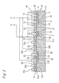
- the main MOSFET 1, the detecting MOSFET 2, the protecting circuit 3, the first impedance element 4 and the protective MOSFET 5 are formed together on one n-type silicon substrate 10.
- the protective MOSFET 5 and the second and third MOSFETs 45 and 46 are not shown in Fig. 3 , the construction of each of these MOSFETs is as same as the construction of the first MOSFET 44.
- the first, third and fourth impedance elements 4, 33 and 34 are also not shown in Fig. 3 , the construction of each of these elements is as same as the construction of the second impedance element 32.
- a drain electrode (not shown) which is connected to the external drain terminal D.
- a lot of small signal MOSFETs are connected to one another in parallel.
- a source region 12 is formed within a p-type well region 11 formed on the n-type silicon substrate 10.
- Gate electrodes 13 of the small signal MOSFETs are commonly connected to one another, while a source electrode 14 is connected to each of the source regions 12.
- a source region 22 is formed within a p-type well region 21 formed on the n-type silicon substrate 10.
- a source electrode 24 is connected to the source regions 22, while a gate electrode 23 is connected to the external gate terminal G.
- a drain region 52 and a source region 53 are formed with an interval therebetween, within a p-type well region 51 formed on the n-type silicon substrate 10.
- a drain electrode 55 is provided on the drain region 52, while a source electrode 56 is provided on the source region 53.
- the gate electrode 13, 23 or 53 of each of the main MOSFET 1, the detecting MOSFET 2 and the first MOSFET 32 is composed of polycrystalline silicon.
- the second impedance element 32 includes a polycrystalline silicon layer 32a and a pair of electrodes 32b and 32c provided on the polycrystalline silicon layer 32a.
- Each of the diodes constituting the diode array 31 includes a polycrystalline silicon layer 31a of a first conductive type (for example, n-type), a polycrystalline silicon layer 31b of a second conductive type (for example, p-type), an electrode 31c provided on the polycrystalline silicon layer 31a and another electrode 31d provided on the polycrystalline silicon layer 31b.
- the size of the semiconductor device may be reduced in comparison with the case that it is constructed by combining discrete parts.
- characteristics of the elements constituting the semiconductor device may be uniformed (For example, characteristics of the protective MOSFET 5 and each of the MOSFETs 44 to 46 may be uniformed.).
- the first impedance element 4, each of the diodes constituting the diode array 31 and each of the impedance elements 32 to 34 in the protecting curcuit3 is composed of polycrystalline silicon which is the material of the gate electrodes of the MOSFETs.
- the semiconductor device with protective functions having the circuit construction shown in Fig. 2 can be manufactured using a general technique for manufacturing a semiconductor so that the process for manufacturing the semiconductor device may be simplified.
- the semiconductor device with protective functions having the circuit construction shown in Fig. 2 may be of course constructed by combining discrete parts.
- each of the MOSFETs constituting the semiconductor device is not a transistor of a current driven type such as a bipolar transistor, but one of a voltage driven type, the MOSFETs can be formed on the single substrate 11.
- the protective circuit 3 operates so as to limit the current flowing the lines between the external drain terminal D and the external source terminal S. Further, if the semiconductor device generates heat so that its temperature rises to or over a predetermined temperature, it becomes OFF. Then the temperature of the semiconductor device lowers below the predetermined temperature, the semiconductor device operates so as to self-return.
- the semiconductor device with protective functions according to Embodiment 2 which is one of three-terminal semiconductor devices, is provided with an external drain terminal D, an external source terminal S and an external gate terminal G.
- the semiconductor device is inserted between a power source and a load.
- a current flowing between the external drain terminal D and the external source terminal S is controlled in accordance with a control voltage applied between the external gate terminal, G and the external source terminal S.
- the external drain terminal D composes the first main terminal, the external source terminal S composing the second main terminal, and the external gate terminal G composing the control terminal.
- the semiconductor device is provided with a main MOSFET 1, first and second detecting MOSFETs 2a and 2b, a protective circuit 3, a first impedance element 4 and a protective MOSFET 5.
- the main MOSFET 1 is inserted between the external drain terminal D and the external source terminal S while it is turned to ON or OFF in accordance with the control voltage.
- the protective MOSFET 5 is inserted between the gate electrode (control electrode) and the source electrode (reference electrode) of the main MOSFET 1.
- Each of the detecting MOSFETs 2a and 2b which is inserted between the external drain terminal D and the protective circuit 3, is turned to ON or OFF in accordance with the control voltage.
- the first impedance element 4 which is composed of a resistance member, is inserted between the protective MOSFET 5 and a junction (or point) connecting the external gate terminal G to the gate electrode (control electrode) of the first detecting MOSFET 2a.
- the power is supplied from the power source to the protective circuit 3 through the external drain terminal D and the detecting MOSFETs 2a and 2b.
- the main MOSFET 1 composes the main transistor of the voltage driven type, the first detecting MOSFET 2a composing the first detection transistor of the voltage driven type, the second detecting MOSFET 2b composing the second detection transistor of the voltage driven type, and the protective MOSFET 5 composing the protective transistor.
- the protective circuit 3 is provided with a diode array 31, second to fourth impedance elements 32-34 and first and second MOSFETs 44 and 45.
- Each of the second and third impedance elements 32 and 33 which is composed of a resistance member, is commonly connected to the source electrode of the first detecting MOSFET 2a at one end portion thereof.
- the fourth impedance element 34 which is composed of a resistance member, is connected to the source electrode of the second detecting MOSFET 2b at one end portion thereof while it is connected to the source electrode of the main MOSFET 1 at the other end portion thereof.
- Each of the first and second MOSFETs 44 and 45 is commonly connected to the source electrode of the main MOSFET 1 at the source electrode thereof.
- the diode array 31, which is thermally connected with the main MOSFET 1, is inserted between the drain electrode and the source electrode of the second MOSFET 45 in such a manner that the anode side of the diode array 31 is connected to the drain electrode of the second MOSFET 45.
- the other end portion of the second impedance element 32 is connected to the drain electrode of the first MOSFET 44.
- the other end portion of the third impedance element 33 is connected to the drain electrode of the second MOSFET 45.
- the gate electrode of the first MOSFET 44 is connected to the drain electrode of the second MOSFET 45.
- the gate electrode of the second MOSFET 45 is connected to the source electrode of the second detecting MOSFET 2b.
- the gate electrode (control electrode) of the protective MOSFET 5 is connected to the drain electrode of the first MOSFET 44.
- the source electrode (reference electrode) of the protective MOSFET 5 is connected to the source electrode of the main MOSFET 1.
- the drain electrode of the protective MOSFET 5 is connected to the gate electrode of the main MOSFET 1.
- the gate electrode of the first detecting MOSFET 2a is connected to the gate electrode of the main MOSFET 1 through the first impedance element 4.
- the gate electrode of the second detecting MOSFET 2b is connected to the gate electrode of the main MOSFET 1.
- each of the main MOSFET 1 and the detecting MOSFETs 2a and 2b becomes ON if the gate voltage (i.e. voltage between the gate electrode and the source electrode) of each of the main MOSFET 1 and the detecting MOSFETs 2a and 2b is equal to or higher than its threshold value.
- the load current flows between the external drain terminal D and the external source terminal S.
- each of the main MOSFET 1 and the detecting MOSFETs 2a and 2b becomes OFF. In this case, the external drain terminal D and the external source terminal S are shut to each other so that the load current does not flow.
- Each of the protective MOSFET 5, the first and second MOSFETs 44 and 45 and the second detecting MOSFET 2b starts to oscillate if voltage equal to or higher than the specified voltage is applied between the external drain terminal D and the external source terminal S so that the voltage caused between the source electrode of the first detecting MOSFET 2a and the external source terminal S becomes equal to or higher than the threshold value of the gate voltage of each of the protective MOSFET 5 and the first MOSFETs 44, when the control voltage is applied between the external gate terminal G and the external source terminal S so that the main MOSFET 1 and the detecting MOSFETs 2a and 2b become ON.
- the protective MOSFET 5 when the protective MOSFET 5 is ON, the gate electrode and the source electrode of the main MOSFET 1 short-circuit to each other so that the main MOSFET 1 becomes OFF.
- the protective MOSFET 5 when the protective MOSFET 5 is OFF, the main MOSFET 1 becomes ON. That is, if voltage equal to or higher than the specified voltage is applied between the external drain terminal D and the external source terminal S when the main MOSFET 1 and the detecting MOSFETs 2a and 2b are ON, the protective circuit 3 makes the main MOSFET 1 perform the ON/OFF operation through the protective MOSFET 5. In consequence, the current flowing through the main MOSFET 1 is limited so that the main MOSFET 1 is protected.
- the diode array 31 is thermally connected with the main MOSFET 1.
- the forward voltage of each of the diodes constituting the diode array 31 has a negative temperature characteristic.
- the main MOSFET 1 generates heat so that its temperature rises, the end-to-end voltage of the diode array 31 lowers.
- the first MOSFET 44 maintains OFF.
- the protective MOSFET 5 maintains ON, and then the gate electrode and the source electrode of the main MOSFET 1 short-circuit to each other so that the main MOSFET 1 maintains OFF.
- the first detecting MOSFET 2a maintains ON if the protective MOSFET 5 is ON, because the first impedance element 4 is inserted between the drain electrode of the protective MOSFET 5 and the junction connecting the external gate terminal G to the gate electrode of the first detecting MOSFET 2a.
- the main MOSFET 1 becomes OFF and then the temperature of the main MOSFET 1 lowers so that the end-to-end voltage of the diode array 31 becomes equal to or high than the threshold voltage of the first MOSFET 44, each of the detective MOSFET 5, the first and second MOSFETs 44 and 45 and the second detecting MOSFET 2 restarts to oscillate.
- the main MOSFET 1 also repeats its ON/OFF operation.
- the action of the detective circuit 3 is stopped so that the main MOSFET 1 becomes ON.
- the current flowing through each of the detecting MOSFETs 2a and 2b is sufficiently smaller in comparison with the current flowing through the main MOSFET 1.
- the protective circuit 3 has the first protective function, the second protective function and the self-returning function as same as those of the protective circuit 3 in Embodiment 1.
- the diode array 31 composes the temperature detecting member.
- the semiconductor device with protective functions according to Embodiment 2 through the external drain terminal D and the detecting MOSFETs 2a and 2b, the power is supplied from the power source to the protective circuit 3 inserted between the external drain terminal D and the external source terminal S, which protects the main MOSFET 1 by the protective MOSFET 5 when the abnormality is detected thereby. Accordingly, it is not necessary to supply the power from the driver to both of the protective circuit 3 and the main MOSFET 1, as different from the conventional semiconductor device with protective functions shown in Fig. 11 . In consequence, the semiconductor device according to Embodiment 2 can operate with a very small gate driving current. Meanwhile, when the abnormality of the main MOSFET 1 has run out, the protective function, which has protected the main MOSFET 1, is automatically dissolved.
- the semiconductor device with protective functions according to Embodiment 2 is also formed on one substrate as same as the case of Embodiment 1, although it is not shown.
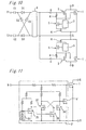
- the fundamental construction of the semiconductor device with protective functions according to Embodiment 3 is nearly as same as that of Embodiment 1.
- the semiconductor device is provided with a non-return diode 6 inserted between the external source terminal S and a junction connecting the protective MOSFET 5 to the protective circuit 3, in such a manner that the non-return diode 6 has polarity to prevent the current from flowing from the external source terminal S to the protective MOSFET 5 and the protective circuit 3.
- each of the constructive members common with that of Embodiment 1 is given the same reference numeral as that of Embodiment 1, and then the description of the member is omitted. Further, the descriptions about operations of the above-mentioned members are also omitted, because they are as same as those of Embodiment 1.
- the source electrode of each of the protective MOSFET 5 and the first to third MOSFETs 44-46 is commonly connected to the anode of the non-return diode 6.
- the cathode of the non-return diode 6 is connected to the external source terminal S.
- its anode side terminal is connected to the gate electrode of the first MOSFET 44, while its cathode side terminal is connected to the source electrode of the main MOSFET 1.
- the source electrode of the main MOSFET 1 is connected to the external source terminal S.
- the main MOSFET 1, the detecting MOSFET 2, the protecting circuit 3, the first impedance element 4, the protective MOSFET 5 and the non-return diode 6 are formed together on one n-type silicon substrate 10, nearly as same as the case of Embodiment 1.
- each of the protective MOSFET 5 and the second and third MOSFETs 45 and 46 are not shown in Fig. 7 , the construction of each of these MOSFETs is as same as the construction of the first MOSFET 44.
- the first, third and fourth impedance elements 4, 33 and 34 are also not shown in Fig. 7 , the construction of each of these elements is as same as the construction of the second impedance element 32.
- the construction of each of the diodes constituting the diode array 31 is also as same as that of Embodiment 1 (see Fig. 3 ).
- a drain electrode (not shown) which is connected to the external drain terminal D.
- each of the constructive members common with that of Embodiment 1 is given the same reference numeral as that of Embodiment 1.
- the non-return diode 6 includes a polycrystalline silicon layer 61 of a first conductive type (for example, n-type), a polycrystalline silicon layer 62 of a second conductive type (for example, p-type), an electrode 63 provided on the polycrystalline silicon layer 61 and another electrode 64 provided on the polycrystalline silicon layer 62.
- a first conductive type for example, n-type
- a polycrystalline silicon layer 62 of a second conductive type for example, p-type
- an electrode 63 provided on the polycrystalline silicon layer 61
- another electrode 64 provided on the polycrystalline silicon layer 62.
- the fundamental construction of the semiconductor device with protective functions according to Embodiment 4 is nearly as same as that of Embodiment 2.
- the semiconductor device is provided with a non-return diode 6 inserted between the external source terminal S and a junction connecting the protective MOSFET 5 to the protective circuit 3, in such a manner that the non-return diode 6 has polarity to prevent the current from flowing from the external source terminal S to the protective MOSFET 5 and the protective circuit 3.
- each of the constructive members common with that of Embodiment 2 is given the same reference numeral as that of Embodiment 2, and then the description of the member is omitted. Further, the descriptions about operations of the above-mentioned members are also omitted, because they are as same as those of Embodiment 2.
- the source electrode of each of the protective MOSFET 5 and the first and second MOSFETs 44 and 45 is commonly connected to the anode of the non-return diode 6.
- the cathode of the non-return diode 6 is connected to the external source terminal S.
- its anode side terminal is connected to the gate electrode of the first MOSFET 44, while its cathode side terminal is connected to the source electrode of the main MOSFET 1.
- the source electrode of the main MOSFET 1 is connected to the external source terminal S.
- the main MOSFET 1, the detecting MOSFETs 2a and 2b, the protecting circuit 3, the first impedance element 4, the protective MOSFET 5 and the non-return diode 6 are formed together on one n-type silicon substrate 10, as same as the case of Embodiment 1.
- the semiconductor device with protective functions according to Embodiment 5 is provided with two semiconductor device components with protective functions according to Embodiment 3.
- their external source electrodes S are commonly connected to each other, while their external gate terminals G are commonly connected to each other.
- each of the constructive members common with that of Embodiment 3 is given the same reference numeral as that of Embodiment 3, and then the description of the member is omitted.
- the semiconductor device with protective functions according to Embodiment 5 is provided with a light emitting element 7 which is turned on or turned off in accordance with an input signal applied between an input terminal T1 and another input terminal T2, and a photovoltaic (or photo electromotive, photoelectric) element 8 composed of a photodiode array which is optically coupled with the light emitting element 7, to generate electromotive force (or electric power).
- the electromotive force (or electric power) of the photovoltaic element 8 is applied between the external gate terminals G and the external source terminals S.
- a charge-discharge circuit 9 is provided between the both terminals of the photovoltaic element 8 and both of the external gate terminals G and the external source terminals S.
- the charge-discharge circuit 9 When the photovoltaic element 8 generates photo electromotive force, the charge-discharge circuit 9 produces high impedance between the both terminals of the photovoltaic element 8 if the photo electromotive force of the photovoltaic element 8 reaches a predetermined voltage. On that occasion, the photo electromotive force of the photovoltaic element 8 is applied between the external gate terminal G and the external source terminal S. Meanwhile, when the photo electromotive force of the photovoltaic element 8 disappears, the charge-discharge circuit 9 forms a path, through which the electric charge stored by the gate capacity of the main MOSFET 1 is discharged, so as to lower rapidly the voltage between the external gate terminal G and the external source terminal S.
- the semiconductor device with protective functions according to Embodiment 5 is provided between the power source and the load while the current flowing through between the both external drain terminals D, D is switched in the two direction, the current does not flow into the protective circuit 3 or protective MOSFET 5 connected to the anode of the non-return diode 6 even if it is designed such that the current can flow from the external source terminals S to the external drain terminals D. In consequence, it may be prevented that the protective circuit 3 or protective MOSFET 5 operates in error. Further, because the electric power is supplied from the power source to each of the protective circuits 3, the semiconductor device can operate with a very small gate driving current utilizing the photo electromotive force of the photovoltaic element 8. Meanwhile, because the light emitting element 7 and the photovoltaic element 8 are provided, the input side and the output side can be insulated to each other.
- the semiconductor device with protective functions according to Embodiment 6 is provided with two semiconductor device components with protective functions according to Embodiment 3.
- their external source electrodes S are commonly connected to each other, while their external gate terminals G are commonly connected to each other.
- each of the constructive members common with that of Embodiment 3 is given the same reference numeral as that of Embodiment 3, and then the description of the member is omitted.
- the semiconductor device with protective functions according to Embodiment 6 is provided with a rectifying circuit including diodes D1-D4, to which an AC (alternating current) signal applied between an input terminal T1 and another input terminal T2 is inputted through capacitors C1 and C2.
- the DC (direct current) voltage, which has been rectified by the rectifying circuit is applied between the external gate terminals G and the external source terminals S.
- one end portion.of the capacitor C1 is connected to the input terminal T1 while the other end portion is connected to an input terminal of the rectifying circuit.
- one end portion of the capacitor C2 is connected to the input terminal T2 while the other end portion is connected to another input terminal of the rectifying circuit.
- a charge-discharge circuit 9 is provided between the both DC output terminals of the rectifying circuit and both of the external gate terminals G and the external source terminals S.
- the charge-discharge circuit 9 produces high impedance between the both DC output terminals of the rectifying circuit. In consequence, the DC output voltage of the rectifying circuit is applied between the external gate terminal G and the external source terminal S. Meanwhile, when the DC output voltage of the rectifying circuit disappears, the charge-discharge circuit 9 forms a path, through which the electric charge stored by the gate capacity of the main MOSFET 1 is discharged, so as to lower rapidly the voltage between the external gate terminal G and the external source terminal S.
- the semiconductor device with protective functions according to Embodiment 6 is provided between the power source and the load while the current flowing through between the both external drain terminals D, D is switched in the two direction, the current does not flow into the protective circuit 3 or protective MOSFET 5 connected to the anode of the non-return diode 6 even if it is designed such that the current can flow from the external source terminals S to the external drain terminals D. In consequence, it may be prevented that the protective circuit 3 or protective MOSFET 5 operates in error. Further, because the electric power is supplied from the power source to each of the protective circuits 3, the semiconductor device can operate with a very small gate driving current utilizing the DC voltage obtained by rectifying the AC signal.
- the transistors such as the main transistor, the detecting transistor or the like, are composed of MOSFETs.
- those transistors may not limited to MOSFETs so that any transistor of a voltage driven type may be used.
- MOS gate devices such as an IGBT may be used instead of the MOSFETs.
- a semiconductor device with protective functions according to the present invention is particularly useful for protecting the semiconductor device, which can obtain only a very little gate driving current, against its overheat, and is suitable for being used for a power device or the like.
Landscapes
- Semiconductor Integrated Circuits (AREA)
- Metal-Oxide And Bipolar Metal-Oxide Semiconductor Integrated Circuits (AREA)
- Electronic Switches (AREA)
- Insulated Gate Type Field-Effect Transistor (AREA)
Abstract
Description
- The present invention relates to a semiconductor device with protective functions, which can operate with a very small gate driving current and further automatically dissolve its protective function when abnormality of a main transistor has run out.
-
US 5,642,252 discloses a semiconductor device according to the preamble portion of theindependent claim 1. - A. semiconductor device with protective functions having a circuit construction, for example shown in
Fig. 11 , is conventionally known and disclosed inEP 1 028 467Fig. 11 , which is one of three-terminal semiconductor devices, is provided with an external drain terminal (first main terminal) D, an external source terminal (second main terminal) S and an external gate terminal (control terminal) .G. The semiconductor device is inserted between a power source and a load. In the semiconductor device, a current flowing between the external drain terminal D and the external source terminal S is controlled in accordance with a control voltage applied between the external gate terminal G and the external source terminal S. - The semiconductor device shown in
Fig. 11 is provided with amain MOSFET 1 which is turned to ON or OFF in accordance with the control voltage and which is inserted between the external drain terminal D and the external source terminal S, and a protective circuit 3' for protecting themain MOSFET 1. Hereupon, the protective circuit 3' is provided with a protective MOSFET 5' inserted between the gate electrode and the source electrode of themain MOSFET 1, adiode array 31 acting as a temperature detector which is thermally connected with themain MOSFET 1, anotherMOSFET 35 connected to thediode array 31 at each of the gate electrode and the source electrode thereof,further MOSFETs MOSFET 37 is connected to the gate electrode of theMOSFET 38, and afurther MOSFET 36 inserted between the drain electrode and source electrode of theMOSFET 37, the gate electrode of theMOSFET 36 being connected to the drain electrode of theMOSFET 35. According to the circuit construction, when the temperature detected by thediode array 31 rises to or over a predetermined value, themain MOSFET 1 is shut, and then the shut state of themain MOSFET 1 is maintained till the input to the external gate terminal G is reset. That is, when the temperature detected by thediode array 31 rises to or over the predetermined value, the gate voltage of theMOSFET 35 becomes lower than a threshold voltage. In consequence, theMOSFET 35 becomes OFF, theMOSFET 36 becomes ON, and each of theMOSFETs 37 and becomes OEF. As the result, the protective MOSFET 5' becomes ON so that the gate electrode and source electrode of themain MOSFET 1 short-circuit, and then themain MOSFET 1 becomes OFF. - In the conventional semiconductor device with protective functions described above, the protective circuit 3' operates using the voltage applied to the gate electrode of the
MOSFET 1 as its power source. Accordingly, it is necessary to supply the power to both of the protective circuit 3' and themain MOSFET 1. In that case, for example, there is required a driver which can supply a gate driving current of at least 0.1 mA. In consequence, there occurs such a disadvantage that it is difficult to drive the semiconductor device using electromotive force of a photovoltaic element which can supply only a very small gate driving current, or to drive the semiconductor device using power obtained by rectifying an alternating signal which is transmitted through capacitors. - Meanwhile, in the conventional semiconductor device with protective functions described above, if the temperature detected by the
diode array 31 rises to or over the predetermined value when themain MOSFET 1 is overheated, themain MOSFET 1 is shut. The shut state of themain MOSFET 1 is maintained till the input to the external gate terminal G is reset. Therefore, when the semiconductor device is restarted (returned), the control voltage applied to the external gate terminal G is required to be reset as 0 V. - Hereupon, it is also possible to perform two-directional switching by providing two semiconductor devices with protective functions shown in
Fig. 11 , and then commonly connecting the external source terminals S to each other while commonly connecting the external gate terminals G to each other. However, in this case, it is feared that when the current flows from the external sources terminal S to the external drain terminal D, the protective MOSFET 5' of the protective circuit 3' may operate in error. - A power MOSFET according to
US 4,893,158 is provided with a protective circuit including a monitor MOSFET whose drain is connected with the drain of the power MOSFET, a monitor resistor connected between the sources of the power and monitor MOSFETs, and a monitor transistor for decreasing a gate voltage of the power MOSFET when a voltage across the monitor resistor exceeds a predetermined level representing a dangerous condition of the device. - The present invention, which has been developed to solve the conventional problems described above, has an object to provide a semiconductor device, with protective functions which can operate with a very small gate driving current and further automatically dissolve its protective function (or protected state) when abnormality of a main transistor has run out. This object is solved by the features of
claim 1. - According to the semiconductor device, through the first main terminal and the detecting transistor, the power is supplied from the power source to the protective circuit inserted between the first main terminal and the second main terminal, which protects the main transistor by the protective transistor when the abnormality is detected thereby. Accordingly, it is not necessary to supply the power from the driver to both of the protective circuit and the main transistor, as different from the conventional case. In consequence, the semiconductor device can operate with a very small gate driving current. Meanwhile, when the abnormality of the main transistor has run out, the protective function, which has protected the main transistor, is automatically dissolved.
- Further, because each of the transistors constituting the semiconductor device is not one of a current driven type such as a bipolar transistor, but one of a voltage driven type, the transistors can be formed on one single (same) substrate.
- A semiconductor device with protective functions may include a non-return diode inserted between the second main terminal and a junction connecting the protective circuit to a reference electrode of the protective transistor, in such a manner that the non-return diode has polarity to prevent a current from flowing from the second main terminal to the protective transistor and the protective circuit.
- According to the semiconductor device, when the current flows from the second main terminal to the first main terminal, it may be prevented that the current flows into the protective circuit. In consequence, it may be prevented that the protective circuit operates in error.
- A semiconductor device with protective functions may have two semiconductor device components inserted between a power source and a load, in each of which an electric current flowing between a first main terminal and a second main terminal is controlled in accordance with a control voltage applied between a control terminal and the second main terminal, the second main terminals of the two semiconductor device components being commonly connected to each other, and the control terminals of the two semiconductor device components being commonly connected to each other. Each of the semiconductor device components is characterized in that it includes (i) a main transistor of a voltage driven type which is turned to ON or OFF in accordance with the control voltage, the main transistor being inserted between the first main terminal and the second main terminal, (ii) a protective transistor of a voltage driven type inserted between a control electrode of the main transistor and a reference electrode of the main transistor, (iii) a protective circuit which protects the main transistor by the protective transistor when abnormality is detected thereby, the protective circuit being inserted between the first main terminal and the second main terminal, (iv) a detecting transistor of a voltage driven type which is turned to ON or OFF in accordance with the control voltage, the detecting transistor being inserted between the first main terminal and the protective circuit, (v) an impedance element inserted between the protective transistor and a junction connecting the control terminal to a control electrode of the detecting transistor, and (vi) a non-return diode inserted between the second main terminal and a junction connecting the protective circuit to a reference electrode of the protective transistor, in such a manner that the non-return diode has polarity to prevent a current from flowing from the second main terminal to the protective transistor and the protective circuit.
- According to the semiconductor device, when the two-directional switching is performed, it may be prevented that the protective circuit operates in error. Meanwhile, through the first main terminal and the detecting transistor, the power is supplied from the power source to the protective circuit inverted between the first main terminal and the second main terminal, which protects the main transistor by the protective transistor when the abnormality is detected thereby. Accordingly, it is not necessary to supply the power from the driver to both of the protective circuit and the main transistor, as different from the conventional case. In consequence, the semiconductor device can operate with a very small gate driving current. Meanwhile, when the abnormality of the main transistor, has run out, the protective function, which has protected the main transistor, is automatically dissolved.
- In the semiconductor device according to the present invention, it is preferable that the device further includes (a) a light emitting element which is turned on or turned off in accordance with a signal inputted thereto, and (b) a photovoltaic element which is optically coupled with the light emitting element to generate electromotive force, wherein (c) the electromotive force is applied between the control terminal and the second main terminal. In that case, the input terminal and the output terminal may be insulated to each other.
- In the semiconductor device according the present invention, it is also preferable that a voltage obtained by rectifying an alternating signal is applied between the control terminal and the second main terminal. In that case, the input terminal and the output terminal may be insulated to each other for a direct current.
- In the semiconductor device according to the present invention, it is also preferable that (a) for each of the main transistor, the detecting transistor and the protective transistor, conductivity between a one side electrode and a further side electrode acting as a reference electrode is actuated (driven) by a potential difference between the further side electrode and a control electrode, (b) the protective circuit including a thermosensible (i.e. heat sensible) element with a negative temperature characteristic, which is composed of semiconductor, the thermosensible element being thermally connected with the main transistor, and a protective circuit transistor of a voltage driven type, its one side electrode being connected to the control electrode of the protective transistor, its further side electrode being connected to one end portion of the thermosensible element and the further side electrode of the protective transistor, and its control electrode being connected to the other end portion of the thermosensible element, wherein (c) the protective circuit transistor is inserted between the first main terminal and the second main terminal so as to be provided with a power through the detecting transistor, the control electrode of the protective circuit transistor being connected in such a manner that conductivity between its both side electrodes is shut in accordance with a potential rise between the first main terminal and the second main terminal. In this case, it is more preferable that the semiconductor device further includes a non-return diode inserted between the second main terminal and the further electrode of each of the protective transistor and the protective circuit transistor, in such a manner that the non-return diode has polarity to prevent a current from flowing from the second main terminal to the protective transistor and the protective circuit. Hereupon, each of the main transistor, the detecting transistor and the protective transistor may be composed of a MOSFET having a drain electrode as the one side electrode, a source electrode as the further side electrode and a gate electrode as the control electrode.
- In the semiconductor it may also be preferable that (a) the detecting transistor is composed of two or more detecting transistor components, while (b) for each of the main transistor, the detecting transistor components and the protective transistor, conductivity between a one side electrode and a further side electrode acting as a reference electrode is actuated (driven) by a potential difference between the further side electrode and a control electrode, (c) the protective circuit including a thermosensible element with a negative temperature characteristic, which is composed of semiconductor, the thermosensible element being thermally connected with the main transistor, and a protective circuit transistor of a voltage driven type, its one side electrode being connected to the control electrode of the protective transistor, its further side electrode being connected to one end portion of the thermosensible element and the further side electrode of the protective transistor, and its control electrode being connected to the other end portion of the thermosensible element, wherein (d) the protective circuit transistor is inserted between the first main terminal and the second main terminal so as to be provided with a power through any one of the detecting transistor components, the control electrode of the protective circuit transistor being connected in such a manner that conductivity between its both side electrodes is shut in accordance with a potential rise between the first main terminal and the second main terminal. In this case, it is more preferable that the semiconductor device further includes a non-return diode inserted between the second main terminal and the further electrode of each of the protective transistor and the protective circuit transistor, in such a manner that the non-return diode has polarity to prevent a current from flowing from the second main terminal to the protective transistor and the protective circuit. Hereupon, each of the main transistor, the detecting transistor components and the protective transistor may be composed of a MOSFET having a drain electrode as the one side electrode, a source electrode as the further side electrode and a gate electrode as the control electrode.
- In the semiconductor device it may also be preferable that (a) each of the main transistor, the detecting transistor and the protective transistor is composed of a MOSFET, while (b) the protective circuit includes second, third and fourth impedance elements, each of which is commonly connected to a source electrode of the detecting transistor at one end portion thereof, first, second and third MOSFETs, each of which is commonly connected to the second main terminal at a source electrode thereof, and a diode array which is thermally connected with the main transistor and inserted between a drain electrode of the second MOSFET and the source electrode of the second MOSFET in such a manner that an anode side of the diode array is connected to the drain electrode of the second MOSFET, wherein (c) a further end portion of the second impedance element is connected to a drain electrode of the first MOSFET, a further end portion of the third impedance element being connected to the drain electrode of the second MOSFET, a further end portion of the fourth impedance element being connected to a drain electrode of the third MOSFET, a gate electrode of the first MOSFET being connected to the drain electrode of the second MOSFET, a gate electrode of the second MOSFET being connected to the drain electrode of the third MOSFET, a gate electrode of the third MOSFET being connected to the drain electrode of the first MOSFET, a gate electrode of the protective transistor being connected to the drain electrode of the first MOSFET, a source electrode of the protective transistor being connected to a source electrode of the main transistor, and a drain electrode of the protective transistor being connected to a gate electrode of the main transistor. In this case, if each of the impedance elements and each of diodes constituting the diode array are formed utilizing materials of the gate electrodes of the MOSFETs, the diode array, each of the impedance elements and each of the MOSFETs can be formed on one single substrate by means of a simple process.
- In the semiconductor device, it may also be preferable that (a) each of the main transistor, the detecting transistor and the protective transistor is composed of a MOSFET, while (b) the protective circuit includes second, third and fourth impedance elements, each of which is commonly connected to a source electrode of the detecting transistor at one end portion thereof, first, second and third MOSFETs, each of which is commonly connected to an anode of the non-return diode at a source electrode thereof, and a diode array which is thermally connected with the main transistor and inserted between a drain electrode of the second MOSFET and a source electrode of the main transistor in such a manner that an anode side of the diode array is connected to the drain electrode of the second MOSFET, wherein (c) a further end portion of the second impedance element is connected to a drain electrode of the first MOSFET, a further end portion of the third impedance element being connected to the drain electrode of the second MOSFET, a further end portion of the fourth impedance element being connected to a drain electrode of the third MOSFET, a gate electrode of the first MOSFET being connected to the drain electrode of the second MOSFET, a gate electrode of the second MOSFET being connected to the drain electrode of the third MOSFET, a gate electrode of the third MOSFET being connected to the drain electrode of the first MOSFET, a gate electrode of the protective transistor being connected to the drain electrode of the first MOSFET, a source electrode of the protective transistor being connected to the source electrode of the main transistor through the non-return diode, and a drain electrode of the protective transistor being connected to a gate electrode of the main transistor. In this case, if the non-return diode, each of the impedance elements and each of diodes constituting the diode array are formed utilizing materials of the gate electrodes of the MOSFETs, these can be formed on one single substrate by means of a simple process.
- In the semiconductor device, it is also preferable that (a) the detecting transistor is composed of a first detection transistor and a second detection transistor, (b) each of the main transistor, the first detection transistor, the second detection transistor and the protective transistor being composed of a MOSFET, (c) the impedance element being defined as a first impedance element, (d) the protective circuit including second and third impedance elements, each of which is commonly connected to a source electrode of the first detection transistor at one end portion thereof, first and second MOSFETs, each of which is commonly connected to a source electrode of the main transistor at a source electrode thereof, a diode array which is thermally connected with the main transistor and inserted between a drain electrode of the second MOSFET and the source electrode of the second MOSFET in such a manner that an anode side of the diode array is connected to the drain electrode of the second MOSFET, and a fourth impedance element which is connected to a source electrode of the second detection transistor at one end portion thereof and to the source electrode of the main transistor at a further end portion thereof, wherein (e) a further end portion of the second impedance element is connected to a drain electrode of the first MOSFET, a further end portion of the third impedance element being connected to the drain electrode of the second MOSFET, a gate electrode of the first MOSFET being connected to the drain electrode of the second MOSFET, a gate electrode of the second MOSFET being connected to the source electrode of the second detection transistor, a gate electrode of the protective transistor being connected to the drain electrode of the first MOSFET, a source electrode of the protective transistor being connected to the source electrode of the main transistor, a drain electrode of the protective transistor being connected to a gate electrode of the main transistor, a gate electrode of the first detection transistor being connected to the gate electrode of the main transistor through the first impedance element, and a gate electrode of the second detection transistor being connected to then gate electrode of the main transistor. In this case, if each of the impedance elements and each of diodes constituting the diode array are formed utilizing materials of the gate electrodes of the MOSFETs, these can be formed on one single substrate by means of a simple process.
- In the semiconductor device, it may also be preferable that (a) the detecting transistor is composed of a first detection transistor and a second detection transistor, (b) each of the main transistor, the first detection transistor, the second detection transistor and the protective transistor being composed of a MOSFET, (c) the impedance element being defined as a first impedance element, (d) the protective circuit including second and third impedance elements, each of which is commonly connected to a source electrode of the first detection transistor at one end portion thereof, first and second MOSFETs, each of which is commonly connected to an anode of the non-return diode at a source electrode thereof, a diode array which is thermally connected with the main transistor and inserted between a drain electrode of the second MOSFET and a source electrode of the main transistor in such a manner that an anode side of the diode array is connected to the drain electrode of the second MOSFET, and a fourth impedance element which is connected to a source electrode of the second detection transistor at one end portion thereof and to the source electrode of the main transistor at a further end portion thereof, wherein (e) a further end portion of the second impedance element is connected to a drain electrode of the first MOSFET, a further end portion of the third impedance element being connected to the drain electrode of the second MOSFET, a gate electrode of the first MOSFET being connected to the drain electrode of the second MOSFET, a gate electrode of the second MOSFET being connected to the source electrode of the second detection transistor, a gate electrode of the protective transistor being connected to the drain electrode of the first MOSFET, a source electrode of the protective transistor being connected to the source electrode of the main transistor through the non-return diode, a drain electrode of the protective transistor being connected to a gate electrode of the main transistor, a gate electrode of the first detection transistor being connected to the gate electrode of the main transistor through the first impedance element, and a gate electrode of the second detection transistor being connected to the gate electrode of the main transistor. In this case, if the non-return diode, each of the impedance elements and each of diodes constituting the diode array are formed utilizing materials of the gate electrodes of the MOSFETs, these can be formed on one single substrate by means of a simple process.
- In the semiconductor device, it may be preferable that the main transistor, the detecting transistor, the protective transistor, the protective circuit and the impedance element are formed on one substrate. In this case, the size of the semiconductor device may be reduced in comparison with such a case that it is constructed by combining discrete parts. Moreover, characteristics of the elements constituting the semiconductor device may be uniformed. Meanwhile, when each of the main transistor, the detecting transistor and the protective transistor is formed as a MOSFET, each of the impedance elements can be formed using polycrystalline silicon which is a material of the gate electrodes of the MOSFETs. In consequence, the process for manufacturing the semiconductor device may be simplified. In addition, when the diode array is provided in the protective circuit, for example as an element for detecting the temperature, each of diodes constituting the diode array can be formed using polycrystalline silicon, which is a material of the gate electrodes of the MOSFETs.
- The present invention will be more sufficiently understood from the detailed explanation described below and the accompanying drawings, and in which:
-
Fig. 1 is a rough circuit diagram of a semiconductor device with protective functions according toEmbodiment 1 of the present invention; -
Fig. 2 is a concrete circuit diagram of the semiconductor device shown inFig. 1 ; -
Fig. 3 is a sectional elevation view of the semiconductor device shown inFig. 1 ; -
Fig. 4 is a concrete circuit diagram of a semiconductor device with protective functions according toEmbodiment 2 of the present invention; -
Fig. 5 is a rough circuit diagram of a semiconductor device with protective functions according toEmbodiment 3 of the present invention; -
Fig. 6 is a concrete circuit diagram of the semiconductor device shown inFig. 5 ; -
Fig. 7 is a sectional elevation view of the semiconductor device shown inFig. 5 ; -
Fig. 8 is a concrete circuit diagram of a semiconductor device with protective functions according toEmbodiment 4 of the present invention; -
Fig. 9 is a rough circuit diagram of a semiconductor device with protective functions according toEmbodiment 5 of the present invention; -
Fig. 10 is a rough circuit diagram of a semiconductor device with protective functions according toEmbodiment 6 of the present invention; and -
Fig. 11 is a circuit diagram of a conventional semiconductor device with protective functions. - This application is based on the patent application No.
2000-300894 - Hereinafter,
Embodiment 1 of the present invention will be described. - As shown in
Fig. 1 , the semiconductor device with protective functions according toEmbodiment 1, which is one of three-terminal semiconductor devices, is provided with an external drain terminal D, an external source terminal S and an external gate terminal G. The semiconductor device is inserted between a power source and a load. In the semiconductor device, a current flowing between the external drain terminal D and the external source terminal S is controlled in accordance with a control voltage applied between the external gate terminal G and the external source terminal S. InEmbodiment 1, the external drain terminal D composes the first main terminal, the external source terminal S composing the second main terminal, and the external gate terminal G composing the control terminal. - The semiconductor device is provided with a
main MOSFET 1, a detectingMOSFET 2, aprotective circuit 3, afirst impedance element 4 and aprotective MOSFET 5. Themain MOSFET 1 is inserted between the external drain terminal D and the external source terminal S while it is turned to ON or OFF (i.e. becomes ON or OFF) in accordance with the control voltage. Theprotective MOSFET 5 is inserted between the gate electrode (control electrode) and the source electrode (reference electrode) of themain MOSFET 1. Theprotective circuit 3, which is inserted between the external drain terminal D and the external source terminal S, protects themain MOSFET 1 by theprotective MOSFET 5 when abnormality is detected thereby. The detectingMOSFET 2, which is inserted between the external drain terminal D and theprotective circuit 3, is turned to ON or OFF (i.e. becomes ON or OFF) in accordance with the control voltage. Thefirst impedance element 4, which is composed of a resistance member, is inserted between theprotective MOSFET 5 and a junction (or point) connecting the external gate terminal G to the gate electrode (control electrode) of the detectingMOSFET 2. - Hereupon, the power (electrical power) is supplied from the power source to the
protective circuit 3 through the external drain terminal D and the detectingMOSFET 2. InEmbodiment 1, themain MOSFET 1 composes the main transistor of the voltage driven type, the detectingMOSFET 2 composing the detecting transistor of the voltage driven type, and theprotective MOSFET 5 composing the protective transistor. -
Fig. 2 shows the circuit shown inFig. 1 more concretely. Theprotective circuit 3 is provided with adiode array 31, second to fourth impedance elements 32-34 and first to third MOSFETs 44-46. Each of the second to fourth impedance elements 32-34, which is composed of a resistance member, is commonly connected to the source electrode of the detectingMOSFET 2 at one end portion thereof. Each of the first to third MOSFETs 44-46 is commonly connected to the external source terminal S at the source electrode thereof. Hereupon, thefirst MOSFET 44 composes the protective circuit transistor. Thediode array 31, which is thermally connected with themain MOSFET 1, is inserted between the drain electrode and the source electrode of thesecond MOSFET 45 in such a manner that the anode side of thediode array 31 is connected to the drain electrode of thesecond MOSFET 45. - In the
protective circuit 3, the other end portion of thesecond impedance element 32 is connected to the drain electrode of thefirst MOSFET 44. The other end portion of thethird impedance element 33 is connected to the drain electrode of thesecond MOSFET 45. The other end portion of thefourth impedance element 34 is connected to the drain electrode of thethird MOSFET 46. The gate electrode of thefirst MOSFET 44 is connected to the drain electrode of thesecond MOSFET 45. The gate electrode of thesecond MOSFET 45 is connected to the drain electrode of thethird MOSFET 46. The gate electrode of thethird MOSFET 46 is connected to the drain electrode of thefirst MOSFET 44. - The gate electrode (control electrode) of the
protective MOSFET 5 is connected to the drain electrode of thefirst MOSFET 44. The source electrode (reference electrode) of theprotective MOSFET 5 is connected to the source electrode of themain MOSFET 1. The drain electrode of theprotective MOSFET 5 is connected to the gate electrode of themain MOSFET 1. - Hereinafter, the operation of the semiconductor device with protective functions according to
Embodiment 1 will be described. When the control voltage is not applied between the external gate terminal G and the external source terminal S, both of themain MOSFET 1 and the detectingMOSFET 2 are OFF so that the current does not flow between the external drain terminal D and the external source terminal S. That is, the load current does not flow. - On the other hand, when the control voltage is applied between the external gate terminal G and the external source terminal S, each of the
main MOSFET 1 and the detectingMOSFET 2 becomes ON if the gate voltage (i.e. voltage between the gate electrode and the source electrode) of each of themain MOSFET 1 and the detectingMOSFET 2 is equal to or higher than its threshold value. In consequence, the load current flows between the external drain terminal D and the external source terminal S. Hereupon, if the application of the control voltage between the external gate terminal G and the external source terminal S is stopped, each of themain MOSFET 1 and the detectingMOSFET 2 becomes OFF. In this case, the external drain terminal D and the external source terminal S are shut to each other so that the load current does not flow. - The
protective circuit 3 is provided with theimpedance elements 32 to 34 and theMOSFETs 44 to 46, which are connected in the manner shown inFig. 2 . The constant of each of theimpedance elements 32 to 34 is set in such a manner that oscillation is caused utilizing parasitic capacitance of each of theMOSFETs 44 to 46 when voltage equal to or higher than the specified voltage is applied between the external drain terminal D and the external source terminal S. Therefore, in theprotective circuit 3, each of theMOSFETs 44 to 46 starts to oscillate if voltage higher than the specified voltage is applied between the external drain terminal D and the external source terminal S so that the voltage caused between the source electrode of the detectingMOSFET 2 and the external source terminal S becomes equal to or higher than the threshold value of the gate voltage of each of theMOSFETs 44 to 46, when the control voltage is applied between the external gate terminal G and the external source terminal S so that themain MOSFET 1 and the detectingMOSFET 2 become ON. Thus, theprotective MOSFET 5 performs (repeats) ON/OFF operation. - Hereupon, when the
protective MOSFET 5 is ON, the gate electrode and the source electrode of themain MOSFET 1 short-circuit to each other so that themain MOSFET 1 becomes OFF. On the other hand, when theprotective MOSFET 5 is OFF, themain MOSFET 1 becomes ON. That is, if voltage equal to or higher than the specified voltage is applied between the external drain terminal D and the external source terminal S when themain MOSFET 1 and the detectingMOSFET 2 are ON, theprotective circuit 3 makes themain MOSFET 1 perform the ON/OFF operation through theprotective MOSFET 5. In consequence, the current flowing through themain MOSFET 1 is limited so that themain MOSFET 1 is protected. - Meanwhile, in the
protective circuit 3, thediode array 31 is thermally connected with themain MOSFET 1. Hereupon, the forward voltage of each of the diodes constituting thediode array 31 has a negative temperature characteristic. In consequence; if themain MOSFET 1 generates heat so that its temperature rises, the end-to-end voltage of thediode array 31 lowers. Hereupon, when the end-to-end voltage of thediode array 31 lowers below the threshold voltage of thefirst MOSFET 44, thefirst MOSFET 44 maintains OFF. In consequence, theprotective MOSFET 5 maintains ON, and then the gate electrode and the source electrode of themain MOSFET 1 short-circuit to each other so that themain MOSFET 1 maintains OFF. - In that case, the detecting
MOSFET 2 maintains ON if theprotective MOSFET 5 is ON, because thefirst impedance element 4 is inserted between the drain electrode of theprotective MOSFET 5 and the junction connecting the external gate terminal G to the gate electrode of the detectingMOSFET 2. Hereupon, when themain MOSFET 1 becomes OFF and then the temperature of themain MOSFET 1 lowers so that the end-to-end voltage of thediode array 31 becomes a voltage equal to or high than the threshold voltage of thesecond MOSFET 45, each of theMOSFETs 44 to 46 restarts to oscillate. As the result, themain MOSFET 1 also repeats its ON/OFF operation. - Thus, the voltage between the external drain terminal D and the external source terminal S lowers below the specified voltage, the action of the
detective circuit 3 is stopped so that themain MOSFET 1 becomes ON. Hereupon, when both of themain MOSFET 1 and the detectingMOSFET 2 are ON in the steady state, the current flowing through the detectingMOSFET 2 is sufficiently smaller in comparison with the current flowing through themain MOSFET 1. Therefore, the power applied to the detectingMOSFET 2 is sufficiently smaller in comparison with the power applied to themain MOSFET 1. - That is, the
protective circuit 3 has the following functions. InEmbodiment 1, thediode array 31 composes the temperature detecting section. - (a) First protective function: When voltage equal to or higher than the specified voltage is applied between the external drain terminal D and the external source terminal S (i.e. When over-current flows through the main MOSFET 1) in the state that the
main MOSFET 1 is ON, theprotective circuit 3 oscillates to make theprotective MOSFET 5 perform its ON/OFF operation, thereby making themain MOSFET 1 perform its ON/OFF operation to protect themain MOSFET 1. - (b) Second protective function: When the temperature detected by the
diode array 31 rises to or over a predetermined value (temperature where the end-to-end voltage of thediode array 31 reaches the threshold voltage of the first MOSFET 44), theprotective circuit 3 makes theprotective MOSFET 5 maintain ON, thereby making themain MOSFET 1 maintain OFF to protect themain MOSFET 1. - (c) Self-returning function: When the detected temperature lowers below the predetermined value (i.e. When the end-to-end voltage of the
diode array 31 becomes lower than the threshold voltage of the first MOSFET 44), the second protective function for protecting themain MOSFET 1 is automatically dissolved. - As described above, in the semiconductor device with protective functions according to
Embodiment 1, through the external drain terminal D and the detectingMOSFET 2, the power is supplied from the power source to theprotective circuit 3 inserted between the external drain terminal D and the external source terminal S, which protects themain MOSFET 1 by theprotective MOSFET 5 when the abnormality is detected thereby. Accordingly, it is not necessary to supply the power from the driver to both of theprotective circuit 3 and themain MOSFET 1, as different from the conventional semiconductor device with protective functions shown inFig. 11 . In consequence, the semiconductor device according toEmbodiment 1 can operate with a very small gate driving current. Meanwhile, when the abnormality of themain MOSFET 1 has run out, the protective function, which has protected themain MOSFET 1, is automatically dissolved. - As shown in
Fig. 3 , in the semiconductor device with protective functions according toEmbodiment 1, themain MOSFET 1, the detectingMOSFET 2, the protectingcircuit 3, thefirst impedance element 4 and theprotective MOSFET 5 are formed together on one n-type silicon substrate 10. Although theprotective MOSFET 5 and the second andthird MOSFETs Fig. 3 , the construction of each of these MOSFETs is as same as the construction of thefirst MOSFET 44. Although the first, third andfourth impedance elements Fig. 3 , the construction of each of these elements is as same as the construction of thesecond impedance element 32. Further, on the back surface of the n-type silicon substrate 10, there is formed a drain electrode (not shown) which is connected to the external drain terminal D. - In the
main MOSFET 1 of the semiconductor device, a lot of small signal MOSFETs are connected to one another in parallel. In each of the small signal MOSFETs, asource region 12 is formed within a p-type well region 11 formed on the n-type silicon substrate 10.Gate electrodes 13 of the small signal MOSFETs are commonly connected to one another, while asource electrode 14 is connected to each of thesource regions 12. - In the detecting
MOSFET 2, asource region 22 is formed within a p-type well region 21 formed on the n-type silicon substrate 10. Asource electrode 24 is connected to thesource regions 22, while agate electrode 23 is connected to the external gate terminal G. - In the
first MOSFET 44, adrain region 52 and asource region 53 are formed with an interval therebetween, within a p-type well region 51 formed on the n-type silicon substrate 10. Adrain electrode 55 is provided on thedrain region 52, while asource electrode 56 is provided on thesource region 53. - The
gate electrode main MOSFET 1, the detectingMOSFET 2 and thefirst MOSFET 32 is composed of polycrystalline silicon. Thesecond impedance element 32 includes apolycrystalline silicon layer 32a and a pair ofelectrodes polycrystalline silicon layer 32a. Each of the diodes constituting thediode array 31 includes apolycrystalline silicon layer 31a of a first conductive type (for example, n-type), apolycrystalline silicon layer 31b of a second conductive type (for example, p-type), anelectrode 31c provided on thepolycrystalline silicon layer 31a and anotherelectrode 31d provided on thepolycrystalline silicon layer 31b. - According to
Embodiment 1, because themain MOSFET 1, the detectingMOSFET 2, theprotective MOSFET 5, theprotective circuit 3 and thefirst impedance element 4 are formed on the single substrate10, the size of the semiconductor device may be reduced in comparison with the case that it is constructed by combining discrete parts. Moreover, characteristics of the elements constituting the semiconductor device may be uniformed (For example, characteristics of theprotective MOSFET 5 and each of theMOSFETs 44 to 46 may be uniformed.). In addition, thefirst impedance element 4, each of the diodes constituting thediode array 31 and each of theimpedance elements 32 to 34 in the protecting curcuit3 is composed of polycrystalline silicon which is the material of the gate electrodes of the MOSFETs. In consequence, the semiconductor device with protective functions having the circuit construction shown inFig. 2 can be manufactured using a general technique for manufacturing a semiconductor so that the process for manufacturing the semiconductor device may be simplified. However, the semiconductor device with protective functions having the circuit construction shown inFig. 2 may be of course constructed by combining discrete parts. - Hereupon, because each of the MOSFETs constituting the semiconductor device is not a transistor of a current driven type such as a bipolar transistor, but one of a voltage driven type, the MOSFETs can be formed on the
single substrate 11. - In the case that the input capacitance of the
main MOSFET 1 is larger so that themain MOSFET 1 cannot follow the oscillation of theprotective circuit 3, if voltage equal to or higher than the specified voltage is applied between the external drain terminal D and the external source terminal S, theprotective circuit 3 operates so as to limit the current flowing the lines between the external drain terminal D and the external source terminal S. Further, if the semiconductor device generates heat so that its temperature rises to or over a predetermined temperature, it becomes OFF. Then the temperature of the semiconductor device lowers below the predetermined temperature, the semiconductor device operates so as to self-return. - Hereinafter,
Embodiment 2 of the present invention will be described. - As shown in
Fig. 4 , the semiconductor device with protective functions according toEmbodiment 2, which is one of three-terminal semiconductor devices, is provided with an external drain terminal D, an external source terminal S and an external gate terminal G. The semiconductor device is inserted between a power source and a load. In the semiconductor device, a current flowing between the external drain terminal D and the external source terminal S is controlled in accordance with a control voltage applied between the external gate terminal, G and the external source terminal S. InEmbodiment 2, the external drain terminal D composes the first main terminal, the external source terminal S composing the second main terminal, and the external gate terminal G composing the control terminal. - The semiconductor device is provided with a
main MOSFET 1, first and second detectingMOSFETs protective circuit 3, afirst impedance element 4 and aprotective MOSFET 5. Themain MOSFET 1 is inserted between the external drain terminal D and the external source terminal S while it is turned to ON or OFF in accordance with the control voltage. Theprotective MOSFET 5 is inserted between the gate electrode (control electrode) and the source electrode (reference electrode) of themain MOSFET 1. Theprotective circuit 3, which is inserted between the external drain terminal D and the external source terminal S, protects themain MOSFET 1 by theprotective MOSFET 5 when abnormality is detected thereby. Each of the detectingMOSFETs protective circuit 3, is turned to ON or OFF in accordance with the control voltage. Thefirst impedance element 4, which is composed of a resistance member, is inserted between theprotective MOSFET 5 and a junction (or point) connecting the external gate terminal G to the gate electrode (control electrode) of the first detectingMOSFET 2a. - In the semiconductor device, the power is supplied from the power source to the
protective circuit 3 through the external drain terminal D and the detectingMOSFETs Embodiment 2, themain MOSFET 1 composes the main transistor of the voltage driven type, the first detectingMOSFET 2a composing the first detection transistor of the voltage driven type, the second detectingMOSFET 2b composing the second detection transistor of the voltage driven type, and theprotective MOSFET 5 composing the protective transistor. - The
protective circuit 3 is provided with adiode array 31, second to fourth impedance elements 32-34 and first andsecond MOSFETs third impedance elements MOSFET 2a at one end portion thereof. Thefourth impedance element 34, which is composed of a resistance member, is connected to the source electrode of the second detectingMOSFET 2b at one end portion thereof while it is connected to the source electrode of themain MOSFET 1 at the other end portion thereof. Each of the first andsecond MOSFETs main MOSFET 1 at the source electrode thereof. Thediode array 31, which is thermally connected with themain MOSFET 1, is inserted between the drain electrode and the source electrode of thesecond MOSFET 45 in such a manner that the anode side of thediode array 31 is connected to the drain electrode of thesecond MOSFET 45. - In the
protective circuit 3, the other end portion of thesecond impedance element 32 is connected to the drain electrode of thefirst MOSFET 44. The other end portion of thethird impedance element 33 is connected to the drain electrode of thesecond MOSFET 45. The gate electrode of thefirst MOSFET 44 is connected to the drain electrode of thesecond MOSFET 45. The gate electrode of thesecond MOSFET 45 is connected to the source electrode of the second detectingMOSFET 2b. - The gate electrode (control electrode) of the
protective MOSFET 5 is connected to the drain electrode of thefirst MOSFET 44. The source electrode (reference electrode) of theprotective MOSFET 5 is connected to the source electrode of themain MOSFET 1. The drain electrode of theprotective MOSFET 5 is connected to the gate electrode of themain MOSFET 1. The gate electrode of the first detectingMOSFET 2a is connected to the gate electrode of themain MOSFET 1 through thefirst impedance element 4. The gate electrode of the second detectingMOSFET 2b is connected to the gate electrode of themain MOSFET 1. - Hereinafter, the operation of the semiconductor device with protective functions according to
Embodiment 2 will be described. When the control voltage is not applied between the external gate terminal G and the external source terminal S, all of themain MOSFET 1 and the detectingMOSFETs - On the other hand, when the control voltage is applied between the external gate terminal G and the external source terminal S, each of the
main MOSFET 1 and the detectingMOSFETs main MOSFET 1 and the detectingMOSFETs main MOSFET 1 and the detectingMOSFETs - Each of the
protective MOSFET 5, the first andsecond MOSFETs MOSFET 2b starts to oscillate if voltage equal to or higher than the specified voltage is applied between the external drain terminal D and the external source terminal S so that the voltage caused between the source electrode of the first detectingMOSFET 2a and the external source terminal S becomes equal to or higher than the threshold value of the gate voltage of each of theprotective MOSFET 5 and thefirst MOSFETs 44, when the control voltage is applied between the external gate terminal G and the external source terminal S so that themain MOSFET 1 and the detectingMOSFETs - Hereupon, when the
protective MOSFET 5 is ON, the gate electrode and the source electrode of themain MOSFET 1 short-circuit to each other so that themain MOSFET 1 becomes OFF. On the other hand, when theprotective MOSFET 5 is OFF, themain MOSFET 1 becomes ON. That is, if voltage equal to or higher than the specified voltage is applied between the external drain terminal D and the external source terminal S when themain MOSFET 1 and the detectingMOSFETs protective circuit 3 makes themain MOSFET 1 perform the ON/OFF operation through theprotective MOSFET 5. In consequence, the current flowing through themain MOSFET 1 is limited so that themain MOSFET 1 is protected. - In the
protective circuit 3, thediode array 31 is thermally connected with themain MOSFET 1. Hereupon, the forward voltage of each of the diodes constituting thediode array 31 has a negative temperature characteristic. In consequence, if themain MOSFET 1 generates heat so that its temperature rises, the end-to-end voltage of thediode array 31 lowers. Hereupon, when the end-to-end voltage of thediode array 31 lowers below the threshold voltage of thefirst MOSFET 44, thefirst MOSFET 44 maintains OFF. As the result, theprotective MOSFET 5 maintains ON, and then the gate electrode and the source electrode of themain MOSFET 1 short-circuit to each other so that themain MOSFET 1 maintains OFF. - In that case, the first detecting
MOSFET 2a maintains ON if theprotective MOSFET 5 is ON, because thefirst impedance element 4 is inserted between the drain electrode of theprotective MOSFET 5 and the junction connecting the external gate terminal G to the gate electrode of the first detectingMOSFET 2a. Hereupon, when themain MOSFET 1 becomes OFF and then the temperature of themain MOSFET 1 lowers so that the end-to-end voltage of thediode array 31 becomes equal to or high than the threshold voltage of thefirst MOSFET 44, each of thedetective MOSFET 5, the first andsecond MOSFETs MOSFET 2 restarts to oscillate. As the result, themain MOSFET 1 also repeats its ON/OFF operation. - Thus, the voltage between the external drain terminal D and the external source terminal S lowers below the specified voltage, the action of the
detective circuit 3 is stopped so that themain MOSFET 1 becomes ON. Hereupon, when all of themain MOSFET 1 and the detectingMOSFETs MOSFETs main MOSFET 1. - That is, the
protective circuit 3 has the first protective function, the second protective function and the self-returning function as same as those of theprotective circuit 3 inEmbodiment 1. InEmbodiment 1 also, thediode array 31 composes the temperature detecting member. - Thus, in the semiconductor device with protective functions according to
Embodiment 2, through the external drain terminal D and the detectingMOSFETs protective circuit 3 inserted between the external drain terminal D and the external source terminal S, which protects themain MOSFET 1 by theprotective MOSFET 5 when the abnormality is detected thereby. Accordingly, it is not necessary to supply the power from the driver to both of theprotective circuit 3 and themain MOSFET 1, as different from the conventional semiconductor device with protective functions shown inFig. 11 . In consequence, the semiconductor device according toEmbodiment 2 can operate with a very small gate driving current. Meanwhile, when the abnormality of themain MOSFET 1 has run out, the protective function, which has protected themain MOSFET 1, is automatically dissolved. - The semiconductor device with protective functions according to
Embodiment 2 is also formed on one substrate as same as the case ofEmbodiment 1, although it is not shown. - Hereinafter,
Embodiment 3 of the present invention will be described. - As shown in
Fig. 5 , the fundamental construction of the semiconductor device with protective functions according toEmbodiment 3 is nearly as same as that ofEmbodiment 1. However, the semiconductor device is provided with anon-return diode 6 inserted between the external source terminal S and a junction connecting theprotective MOSFET 5 to theprotective circuit 3, in such a manner that thenon-return diode 6 has polarity to prevent the current from flowing from the external source terminal S to theprotective MOSFET 5 and theprotective circuit 3. Hereupon, each of the constructive members common with that ofEmbodiment 1 is given the same reference numeral as that ofEmbodiment 1, and then the description of the member is omitted. Further, the descriptions about operations of the above-mentioned members are also omitted, because they are as same as those ofEmbodiment 1. - As shown in
Fig. 6 , in the semiconductor device with protective functions according toEmbodiment 3, the source electrode of each of theprotective MOSFET 5 and the first to third MOSFETs 44-46 is commonly connected to the anode of thenon-return diode 6. The cathode of thenon-return diode 6 is connected to the external source terminal S. Regarding to thediode array 31, its anode side terminal is connected to the gate electrode of thefirst MOSFET 44, while its cathode side terminal is connected to the source electrode of themain MOSFET 1. The source electrode of themain MOSFET 1 is connected to the external source terminal S. - As shown in
Fig. 7 , in the semiconductor device with protective functions according toEmbodiment 3 also, themain MOSFET 1, the detectingMOSFET 2, the protectingcircuit 3, thefirst impedance element 4, theprotective MOSFET 5 and thenon-return diode 6 are formed together on one n-type silicon substrate 10, nearly as same as the case ofEmbodiment 1. - Although the
protective MOSFET 5 and the second andthird MOSFETs Fig. 7 , the construction of each of these MOSFETs is as same as the construction of thefirst MOSFET 44. Although the first, third andfourth impedance elements Fig. 7 , the construction of each of these elements is as same as the construction of thesecond impedance element 32. Meanwhile, the construction of each of the diodes constituting thediode array 31 is also as same as that of Embodiment 1 (seeFig. 3 ). Further, on the back surface of the n-type silicon substrate 10, there is formed a drain electrode (not shown) which is connected to the external drain terminal D. InFig.7 , each of the constructive members common with that ofEmbodiment 1 is given the same reference numeral as that ofEmbodiment 1. - The
non-return diode 6 includes apolycrystalline silicon layer 61 of a first conductive type (for example, n-type), apolycrystalline silicon layer 62 of a second conductive type (for example, p-type), anelectrode 63 provided on thepolycrystalline silicon layer 61 and anotherelectrode 64 provided on thepolycrystalline silicon layer 62. - In the case that two semiconductor devices with protective functions according to
Embodiment 3 are provided while their external source terminals S are commonly connected to each other, the action of the parasitic bipolar transistor of each of the MOSFETs 44-46 in theprotective circuit 3 is prevented because thenon-return diode 6 is provided. InFig. 7 , the parasitic bipolar transistor Tr of thefirst MOSFET 44 is schematically shown. - Hereinafter,
Embodiment 4 of the present invention will be described. - As shown in
Fig. 8 , the fundamental construction of the semiconductor device with protective functions according toEmbodiment 4 is nearly as same as that ofEmbodiment 2. However, the semiconductor device is provided with anon-return diode 6 inserted between the external source terminal S and a junction connecting theprotective MOSFET 5 to theprotective circuit 3, in such a manner that thenon-return diode 6 has polarity to prevent the current from flowing from the external source terminal S to theprotective MOSFET 5 and theprotective circuit 3. Hereupon, each of the constructive members common with that ofEmbodiment 2 is given the same reference numeral as that ofEmbodiment 2, and then the description of the member is omitted. Further, the descriptions about operations of the above-mentioned members are also omitted, because they are as same as those ofEmbodiment 2. - As apparent from
Fig. 8 , in the semiconductor device with protective functions according toEmbodiment 4, the source electrode of each of theprotective MOSFET 5 and the first andsecond MOSFETs non-return diode 6. The cathode of thenon-return diode 6 is connected to the external source terminal S. Regarding to thediode array 31, its anode side terminal is connected to the gate electrode of thefirst MOSFET 44, while its cathode side terminal is connected to the source electrode of themain MOSFET 1. The source electrode of themain MOSFET 1 is connected to the external source terminal S. - In the semiconductor device with protective functions according to
Embodiment 4 also, themain MOSFET 1, the detectingMOSFETs circuit 3, thefirst impedance element 4, theprotective MOSFET 5 and thenon-return diode 6 are formed together on one n-type silicon substrate 10, as same as the case ofEmbodiment 1. - In the case that two semiconductor devices with protective functions according to
Embodiment 4 are provided while their external source terminals S are commonly connected to each other, the action of the parasitic bipolar transistor of each of the first andsecond MOSFETs protective circuit 3 is prevented because thenon-return diode 6 is provided. - Hereinafter,
Embodiment 5 of the present invention will be described. - As shown in
Fig. 9 , the semiconductor device with protective functions according toEmbodiment 5 is provided with two semiconductor device components with protective functions according toEmbodiment 3. Regarding to the two semiconductor device components, their external source electrodes S are commonly connected to each other, while their external gate terminals G are commonly connected to each other. Hereupon, each of the constructive members common with that ofEmbodiment 3 is given the same reference numeral as that ofEmbodiment 3, and then the description of the member is omitted. - In addition, the semiconductor device with protective functions according to
Embodiment 5 is provided with alight emitting element 7 which is turned on or turned off in accordance with an input signal applied between an input terminal T1 and another input terminal T2, and a photovoltaic (or photo electromotive, photoelectric)element 8 composed of a photodiode array which is optically coupled with thelight emitting element 7, to generate electromotive force (or electric power). The electromotive force (or electric power) of thephotovoltaic element 8 is applied between the external gate terminals G and the external source terminals S. Further, a charge-discharge circuit 9 is provided between the both terminals of thephotovoltaic element 8 and both of the external gate terminals G and the external source terminals S. When thephotovoltaic element 8 generates photo electromotive force, the charge-discharge circuit 9 produces high impedance between the both terminals of thephotovoltaic element 8 if the photo electromotive force of thephotovoltaic element 8 reaches a predetermined voltage. On that occasion, the photo electromotive force of thephotovoltaic element 8 is applied between the external gate terminal G and the external source terminal S. Meanwhile, when the photo electromotive force of thephotovoltaic element 8 disappears, the charge-discharge circuit 9 forms a path, through which the electric charge stored by the gate capacity of themain MOSFET 1 is discharged, so as to lower rapidly the voltage between the external gate terminal G and the external source terminal S. - Thus, in the case that the semiconductor device with protective functions according to
Embodiment 5 is provided between the power source and the load while the current flowing through between the both external drain terminals D, D is switched in the two direction, the current does not flow into theprotective circuit 3 orprotective MOSFET 5 connected to the anode of thenon-return diode 6 even if it is designed such that the current can flow from the external source terminals S to the external drain terminals D. In consequence, it may be prevented that theprotective circuit 3 orprotective MOSFET 5 operates in error. Further, because the electric power is supplied from the power source to each of theprotective circuits 3, the semiconductor device can operate with a very small gate driving current utilizing the photo electromotive force of thephotovoltaic element 8. Meanwhile, because thelight emitting element 7 and thephotovoltaic element 8 are provided, the input side and the output side can be insulated to each other. - Hereinafter,
Embodiment 6 of the present invention will be described. - As shown in
Fig. 10 , the semiconductor device with protective functions according toEmbodiment 6 is provided with two semiconductor device components with protective functions according toEmbodiment 3. Regarding to the two semiconductor device components, their external source electrodes S are commonly connected to each other, while their external gate terminals G are commonly connected to each other. Hereupon, each of the constructive members common with that ofEmbodiment 3 is given the same reference numeral as that ofEmbodiment 3, and then the description of the member is omitted. - In addition, the semiconductor device with protective functions according to
Embodiment 6 is provided with a rectifying circuit including diodes D1-D4, to which an AC (alternating current) signal applied between an input terminal T1 and another input terminal T2 is inputted through capacitors C1 and C2. The DC (direct current) voltage, which has been rectified by the rectifying circuit is applied between the external gate terminals G and the external source terminals S. Hereupon, one end portion.of the capacitor C1 is connected to the input terminal T1 while the other end portion is connected to an input terminal of the rectifying circuit. Meanwhile, one end portion of the capacitor C2 is connected to the input terminal T2 while the other end portion is connected to another input terminal of the rectifying circuit. - Further, a charge-discharge circuit 9 is provided between the both DC output terminals of the rectifying circuit and both of the external gate terminals G and the external source terminals S. When the DC output voltage of the rectifying circuit reaches a predetermined voltage, the charge-discharge circuit 9 produces high impedance between the both DC output terminals of the rectifying circuit. In consequence, the DC output voltage of the rectifying circuit is applied between the external gate terminal G and the external source terminal S. Meanwhile, when the DC output voltage of the rectifying circuit disappears, the charge-discharge circuit 9 forms a path, through which the electric charge stored by the gate capacity of the
main MOSFET 1 is discharged, so as to lower rapidly the voltage between the external gate terminal G and the external source terminal S. - Thus, in the case that the semiconductor device with protective functions according to
Embodiment 6 is provided between the power source and the load while the current flowing through between the both external drain terminals D, D is switched in the two direction, the current does not flow into theprotective circuit 3 orprotective MOSFET 5 connected to the anode of thenon-return diode 6 even if it is designed such that the current can flow from the external source terminals S to the external drain terminals D. In consequence, it may be prevented that theprotective circuit 3 orprotective MOSFET 5 operates in error. Further, because the electric power is supplied from the power source to each of theprotective circuits 3, the semiconductor device can operate with a very small gate driving current utilizing the DC voltage obtained by rectifying the AC signal. - In Embodiments 1-6 described above, the transistors such as the main transistor, the detecting transistor or the like, are composed of MOSFETs. However, those transistors may not limited to MOSFETs so that any transistor of a voltage driven type may be used. For example, instead of the MOSFETs, MOS gate devices such as an IGBT may be used.
- Although the present invention is described above taking specific embodiments as examples, it will be understood by those skilled in the art that the present invention is not limited to these embodiments, but covers all modifications which are within the scope of the present invention as defined by the appended claims.
- As described above, a semiconductor device with protective functions according to the present invention is particularly useful for protecting the semiconductor device, which can obtain only a very little gate driving current, against its overheat, and is suitable for being used for a power device or the like.
Claims (11)
- A semiconductor device with protective functions inserted between a power source and a load, in which an electric current flowing between a first main terminal (D) and a second main terminal (S) is controlled in accordance with a control voltage applied between a control terminal (G) and said second main terminal (S) comprising:a main transistor (1) of a voltage driven type which is turned to ON or OFF in accordance with said control voltage, said main transistor (1) being inserted between said first main terminal (D) and said second main terminal (S);a protective transistor (5) of a voltage driven type inserted between a control electrode of said main transistor (1) and a reference electrode of said main transistor (1), the reference electrode being connected to the second main terminal (S);a protective circuit (3) which protects said main transistor (1) by said protective transistor (5) when abnormality is detected thereby, said protective circuit (3) being inserted between said first main terminal (D) and said second main terminal (S);a detecting transistor (2) of a voltage driven type is turned to ON or OFF in accordance with said control voltage, said detecting transistor (2) being inserted between said first main terminal (D) and said protective circuit (3); andan impedance element (4) inserted between said protective transistor (5) and a junction connecting said control terminal (G) to a control electrode of said detecting transistor (2), wherein
said protective circuit (3) comprisesa thermosensible element (31) with a negative temperature characteristic, which is composed of semiconductor and to which power is supplied from said power source through said first main terminal (D) and said detecting transistor (2), said thermosensible element (31) being thermally connected with said main transistor (1), characterized in that said protective circuit (3) further comprisesa protective circuit transistor (44) of a voltage driven type to which power is supplied from said power source through said first main terminal (D) and said detecting transistor (2), its one side electrode being connected to the control electrode of said protective transistor (5), its further side electrode being connected to the second main terminal (S), one end portion of said thermosensible element (31) and a reference electrode of said protective transistor (5), and its control electrode being connected to the other end portion of said thermosensible element (31). - The semiconductor device according to claim 1, wherein
for each of said main transistor (1), said detecting transistor (2), said protective transistor (5) and said protective circuit transistor (44), conductivity between a one side electrode and a further side electrode acting as a reference electrode is actuated by a potential difference between said further side electrode and a control electrode, and wherein
the control electrode of said protective circuit transistor (44) is connected in such a manner that conductivity between the one side electrode and the further side electrode of said protective circuit transistor (44) is shut in accordance with a potential rise between said first main terminal (D) and said second main terminal (S). - The semiconductor device according to claim 2, further comprising a non-return diode (6) inserted between said second main terminal (S) and the further electrode of each of said protective transistor (5) and said protective circuit transistor (44), in such a manner that said non-return diode (6) has polarity to prevent current from flowing from said second main terminal (S) to said protective transistor (5) and said protective circuit (3), wherein said one end portion of said thermosensible element (31) is connected between said non-return diode (6) and said second main terminal (S).
- The semiconductor device according to claim 2 or 3, wherein each of said main transistor (1), said detecting transistor (2) and said protective transistor (5) is composed of a MOSFET having a drain electrode as said one side electrode, a source electrode as said further side electrode and a gate electrode as said control electrode.
- The semiconductor device according to claim 1, wherein
said detecting transistor (2) is composed of two or more detecting transistor components (2a, 2b), while
for each of said main transistor (1), said detecting transistor components (2a, 2b) and said protective transistor (5), conductivity between a one side electrode and a further side electrode acting as a reference electrode is actuated by a potential difference between said further side electrode and a control electrode, wherein
said protective circuit transistor (44) is inserted between said first main terminal (D) and said second main terminal (S) so as to be provided with a power through any one of said detecting transistor components (2a, 2b), the control electrode of said protective circuit transistor (44) being connected in such a manner that conductivity between its both side electrodes is shut in accordance with a potential rise between said first main terminal (D) and said second main terminal (S). - The semiconductor device according to claim 5, further comprising a non-return diode (6) inserted between said second main terminal (S) and the further electrode of each of said protective transistor (5) and said protective circuit transistor (44), in such a manner that said non-return diode (6) has polarity to prevent a current from flowing from said second main terminal (S) to said protective transistor (5) and said protective circuit (3), wherein said one end portion of said thermosensible element (31) is connected between said non-return diode (6) and said second main terminal (S).
- The semiconductor device according to claim 5 or 6, wherein each of said main transistor (1), said detecting transistor components (2a, 2b) and said protective transistor (5) is composed of a MOSFET having a drain electrode as said one side electrode, a source electrode as said further side electrode and a gate electrode as said control electrode.
- The semiconductor device according to claim 1, wherein
each of said main transistor (1), said detecting transistor (2) and said protective transistor (5) is composed of a MOSFET, while said protective circuit (3) comprises:second, third and fourth impedance elements (32, 33, 34), each of which is commonly connected to a source electrode of said detecting transistor (2) at one end portion thereof;a first MOSFET as said protective circuit transistor (44) and second and third MOSFETs (45, 46), each of which is commonly connected to said second main terminal (S) at a source electrode thereof; anda diode array as said thermosensible element (31) with the negative temperature characteristic, which is thermally connected with said main transistor (1) and inserted between a drain electrode of said second MOSFET (45) and the source electrode of said second MOSFET (45) in such a manner that an anode side of said diode array is connected to the drain electrode of said second MOSFET (45), whereina further end portion of said second impedance element (32) is connected to a drain electrode of said first MOSFET (44), a further end portion of said third impedance element (33) being connected to the drain electrode of said second MOSFET (45), a further end portion of said fourth impedance element (34) being connected to a drain electrode of said third MOSFET (46), a gate electrode of said first MOSFET (44) being connected to the drain electrode of said second MOSFET (45), a gate electrode of said second MOSFET (45) being connected to the drain electrode of said third MOSFET (46), a gate electrode of said third MOSFET (46) being connected to the drain electrode of said first MOSFET (44), a gate electrode of said protective transistor (5) being connected to the drain electrode of said first MOSFET (44), a source electrode of said protective transistor (5) being connected to a source electrode of said main transistor (1), and a drain electrode of said protective transistor (5) being connected to a gate electrode of said main transistor (1). - The semiconductor device according to claim 1, wherein
said detecting transistor (2) is composed of a first detection transistor (2a) and a second detection transistor (2b), each of said main transistor (1), said first detection transistor (2a), said second detection transistor (2b) and said protective transistor (5) being composed of a MOSFET, said impedance element (4) being defined as a first impedance element, said protective circuit (3) comprising:second and third impedance elements (32, 33), each of which is commonly connected to a source electrode of said first detection transistor (2a) at one end portion thereof;a first MOSFET (44) as said protective circuit transistor (44) and a second MOSFET (45), each of which is commonly connected to a source electrode of said main transistor (1) at a source electrode thereof;a diode array as said thermosensible element (31) with the negative temperature characteristic, which is thermally connected with said main transistor (1) and inserted between a drain electrode of said second MOSFET (45) and the source electrode of said second MOSFET (45) in such a manner that an anode side of said diode array is connected to the drain electrode of said second MOSFET (45); anda fourth impedance element (34) which is connected to a source electrode of said second detection transistor (2b) at one end portion thereof and to the source electrode of said main transistor (1) at a further end portion thereof, whereina further end portion of said second impedance element (32) is connected to a drain electrode of said first MOSFET (44), a further end portion of said third impedance element (33) being connected to the drain electrode of said second MOSFET (45), a gate electrode of said first MOSFET (44) being connected to the drain electrode of said second MOSFET (45) , a gate electrode of said second MOSFET (45) being connected to the source electrode of said second detection transistor (2b), a gate electrode of said protective transistor (5) being connected to the drain electrode of said first MOSFET (44) , a source electrode of said protective transistor (5) being connected to the source electrode of said main transistor (1), a drain electrode of said protective transistor (5) being connected to a gate electrode of said main transistor (1), a gate electrode of said first detection transistor (2a) being connected to the gate electrode of said main transistor (1) through said first impedance element (4), and a gate electrode of said second detection transistor (2b) being connected to the gate electrode of said main transistor (1). - The semiconductor device according to claim 1, further comprising,
a non-return diode (6) inserted between said second main terminal (S) and a junction connecting said protective circuit (3) to a reference electrode of said protective transistor (5), in such a manner that said non-return diode (6) has polarity to prevent a current from flowing from said second main terminal (S) to said protective transistor (5) and said protective circuit (3), wherein said one end portion of said thermosensible element (31) is connected between said non-return diode (6) and said second main terminal (S), and wherein
each of said main transistor (1) , said detecting transistor (2) and said protective transistor (5) is composed of a MOSFET, while said protective circuit (3) comprises:second, third and fourth impedance (32, 33, 34) elements, each of which is commonly connected to a source electrode of said detecting transistor (2) at one end portion thereof;a first MOSFET as said protective circuit transistor (44) and second and third MOSFETs (45, 46), each of which is commonly connected to an anode of said non-return diode (6) at a source electrode thereof; anda diode array as said thermosensible element (31) with the negative temperature characteristic, which is thermally connected with said main transistor (1) and inserted between a drain electrode of said second MOSFET (45) and a source electrode of said main transistor (1) in such a manner that an anode side of said diode array (31) is connected to the drain electrode of said second MOSFET (45), whereina further end portion of said second impedance element (32) is connected to a drain electrode of said first MOSFET (44), a further end portion of said third impedance element (33) being connected to the drain electrode of said second MOSFET (45), a further end portion of said fourth impedance element (34) being connected to a drain electrode of said third MOSFET (46), a gate electrode of said first MOSFET (44) being connected to the drain electrode of said second MOSFET (45), a gate electrode of said second MOSFET (45) being connected to the drain electrode of said third MOSFET (46), a gate electrode of said third MOSFET (46) being connected to the drain electrode of said first MOSFET (44), a gate electrode of said protective transistor (5) being connected to the drain electrode of said first MOSFET (44), a source electrode of said' protective transistor (5) being connected to the source electrode of said main transistor (1) through said non-return diode (6), and a drain electrode of said protective transistor (5) being connected to a gate electrode of said main transistor (1). - The semiconductor device according to claim 1, further comprising,
a non-return diode (6) inserted between said second main terminal (S) and a junction connecting said protective circuit (3) to a reference electrode of said protective transistor (5), in such a manner that said non-return diode (6) has polarity to prevent a current from flowing from said second main terminal (S) to said protective transistor (5) and said protective circuit (3), wherein said one end portion of said thermosensible element (31) is connected between said non-return diode (6) and said second main terminal (S), and wherein
said detecting transistor (2) is composed of a first detection transistor (2a) and a second detection transistor (2b), each of said main transistor (1), said first detection transistor (2a), said second detection transistor (2b) and said protective transistor (5) being composed of a MOSFET, said impedance element being defined as a first impedance element, said protective circuit (3) comprising:second and third impedance elements (32, 33), each of which is commonly connected to a source electrode of said first detection transistor (2a) at one end portion thereof;a first MOSFET (44) as said protective circuit transistor (44) and a second MOSFET (45), each of which is commonly connected to an anode of said non-return diode (6) at a source electrode thereof;a diode array as said thermosensible element (31) with the negative temperature characteristic, which is thermally connected with said main transistor (1) and inserted between a drain electrode of said second MOSFET (45) and a source electrode of said main transistor (1) in such a manner that an anode side of said diode array is connected to the drain electrode of said second MOSFET (45); anda fourth impedance element (34) which is connected to a source electrode of said second detection transistor (2b) at one end portion thereof and to the source electrode of said main transistor (1) at a further end portion thereof, whereina further end portion of said second impedance element is connected to a drain electrode of said first MOSFET (44), a further end portion of said third impedance element (33) being connected to the drain electrode of said second MOSFET (45), a gate electrode of said first MOSFET (44) being connected to the drain electrode of said second MOSFET (45), a gate electrode of said second MOSFET (45) being connected to the source electrode of said second detection transistor (2b), a gate electrode of said protective transistor (5) being connected to the drain electrode of said first MOSFET (44), a source electrode of said protective transistor (5) being connected to the source electrode of said main transistor (1) through said non-return diode (6), a drain electrode of said protective transistor (5) being connected to a gate electrode of said main transistor (1), a gate electrode of said first detection transistor (2a) being connected to the gate electrode of said main transistor (1) through said first impedance element, and a gate electrode of said second detection transistor (2b) being connected to the gate electrode of said main transistor (1).
Applications Claiming Priority (3)
| Application Number | Priority Date | Filing Date | Title |
|---|---|---|---|
| JP2000300894 | 2000-09-29 | ||
| JP2000300894 | 2000-09-29 | ||
| PCT/JP2001/008419 WO2002029949A2 (en) | 2000-09-29 | 2001-09-27 | Semiconductor device with protective functions |
Publications (2)
| Publication Number | Publication Date |
|---|---|
| EP1366552A2 EP1366552A2 (en) | 2003-12-03 |
| EP1366552B1 true EP1366552B1 (en) | 2011-11-09 |
Family
ID=18782508
Family Applications (1)
| Application Number | Title | Priority Date | Filing Date |
|---|---|---|---|
| EP01970240A Expired - Lifetime EP1366552B1 (en) | 2000-09-29 | 2001-09-27 | Semiconductor device with protective functions |
Country Status (5)
| Country | Link |
|---|---|
| US (1) | US6930870B2 (en) |
| EP (1) | EP1366552B1 (en) |
| JP (1) | JP4529353B2 (en) |
| KR (1) | KR100599214B1 (en) |
| WO (1) | WO2002029949A2 (en) |
Families Citing this family (22)
| Publication number | Priority date | Publication date | Assignee | Title |
|---|---|---|---|---|
| EP2009676B8 (en) | 2002-05-08 | 2012-11-21 | Phoseon Technology, Inc. | A semiconductor materials inspection system |
| WO2006072071A2 (en) | 2004-12-30 | 2006-07-06 | Phoseon Technology Inc. | Methods and systems relating to light sources for use in industrial processes |
| US6800802B2 (en) * | 2002-11-09 | 2004-10-05 | Novaest Optitronix Inc. | Circuit device for solar energy application |
| US7524085B2 (en) * | 2003-10-31 | 2009-04-28 | Phoseon Technology, Inc. | Series wiring of highly reliable light sources |
| US7819550B2 (en) | 2003-10-31 | 2010-10-26 | Phoseon Technology, Inc. | Collection optics for led array with offset hemispherical or faceted surfaces |
| JP4765252B2 (en) * | 2004-01-13 | 2011-09-07 | 株式会社豊田自動織機 | Semiconductor device with temperature detection function |
| TWI312583B (en) | 2004-03-18 | 2009-07-21 | Phoseon Technology Inc | Micro-reflectors on a substrate for high-density led array |
| EP1743384B1 (en) | 2004-03-30 | 2015-08-05 | Phoseon Technology, Inc. | Led array having array-based led detectors |
| TWI302756B (en) | 2004-04-19 | 2008-11-01 | Phoseon Technology Inc | Imaging semiconductor structures using solid state illumination |
| JP4706462B2 (en) * | 2005-12-07 | 2011-06-22 | トヨタ自動車株式会社 | Semiconductor device having current detection function |
| DE102006008292B4 (en) * | 2006-02-22 | 2011-09-15 | Infineon Technologies Ag | Overload protection for controllable power consumers |
| JP4887180B2 (en) * | 2007-02-27 | 2012-02-29 | 新日本無線株式会社 | Semiconductor device with short-circuit protection function |
| JP5027680B2 (en) * | 2008-01-18 | 2012-09-19 | パナソニック株式会社 | Semiconductor relay module |
| WO2015025422A1 (en) | 2013-08-23 | 2015-02-26 | 三菱電機株式会社 | Semiconductor device |
| KR101752044B1 (en) * | 2015-01-21 | 2017-06-28 | 주식회사 엘지화학 | Apparatus and method for controlling field effect transistor |
| JP6406464B2 (en) * | 2016-02-18 | 2018-10-17 | 富士電機株式会社 | Insulated gate semiconductor device |
| CN108871608B (en) * | 2017-05-12 | 2020-08-25 | 中芯国际集成电路制造(上海)有限公司 | Semiconductor device and method for detecting heat generation of device |
| JP6922563B2 (en) * | 2017-08-31 | 2021-08-18 | 富士電機株式会社 | Semiconductor device |
| US11063465B2 (en) * | 2018-01-30 | 2021-07-13 | Novatel Inc. | Switching mode front end surge protection circuit |
| WO2019169611A1 (en) * | 2018-03-08 | 2019-09-12 | Texas Instruments Incorporated | Adaptive thermal overshoot and current limiting protection for mosfets |
| US10833668B2 (en) * | 2019-03-07 | 2020-11-10 | Analog Devices International Unlimited Company | Integrated and distributed over temperature protection for power management switches |
| JP7732280B2 (en) * | 2021-08-27 | 2025-09-02 | 富士電機株式会社 | Semiconductor Module |
Citations (1)
| Publication number | Priority date | Publication date | Assignee | Title |
|---|---|---|---|---|
| US5642252A (en) * | 1993-08-18 | 1997-06-24 | Hitachi, Ltd. | Insulated gate semiconductor device and driving circuit device and electronic system both using the same |
Family Cites Families (5)
| Publication number | Priority date | Publication date | Assignee | Title |
|---|---|---|---|---|
| US4893158A (en) * | 1987-06-22 | 1990-01-09 | Nissan Motor Co., Ltd. | MOSFET device |
| JP3180831B2 (en) * | 1991-03-22 | 2001-06-25 | 富士電機株式会社 | Insulated gate control semiconductor device |
| JPH04365373A (en) * | 1991-06-13 | 1992-12-17 | Nec Corp | Semiconductor integrated circuit device |
| JP2801825B2 (en) | 1993-01-14 | 1998-09-21 | 株式会社東芝 | Photo coupler device |
| US6392859B1 (en) | 1999-02-14 | 2002-05-21 | Yazaki Corporation | Semiconductor active fuse for AC power line and bidirectional switching device for the fuse |
-
2001
- 2001-09-27 KR KR1020037004532A patent/KR100599214B1/en not_active Expired - Fee Related
- 2001-09-27 JP JP2002533452A patent/JP4529353B2/en not_active Expired - Fee Related
- 2001-09-27 WO PCT/JP2001/008419 patent/WO2002029949A2/en not_active Ceased
- 2001-09-27 EP EP01970240A patent/EP1366552B1/en not_active Expired - Lifetime
- 2001-09-27 US US10/380,171 patent/US6930870B2/en not_active Expired - Fee Related
Patent Citations (1)
| Publication number | Priority date | Publication date | Assignee | Title |
|---|---|---|---|---|
| US5642252A (en) * | 1993-08-18 | 1997-06-24 | Hitachi, Ltd. | Insulated gate semiconductor device and driving circuit device and electronic system both using the same |
Also Published As
| Publication number | Publication date |
|---|---|
| EP1366552A2 (en) | 2003-12-03 |
| KR20030048051A (en) | 2003-06-18 |
| WO2002029949A3 (en) | 2003-10-09 |
| US6930870B2 (en) | 2005-08-16 |
| JP2004515911A (en) | 2004-05-27 |
| US20040051145A1 (en) | 2004-03-18 |
| JP4529353B2 (en) | 2010-08-25 |
| KR100599214B1 (en) | 2006-07-12 |
| WO2002029949A2 (en) | 2002-04-11 |
Similar Documents
| Publication | Publication Date | Title |
|---|---|---|
| EP1366552B1 (en) | Semiconductor device with protective functions | |
| US4994904A (en) | MOSFET having drain voltage detection function | |
| US6215634B1 (en) | Drive circuit for power device | |
| US7924084B2 (en) | Semiconductor device | |
| EP0784376B1 (en) | Semiconductor device and semiconductor module | |
| US7310213B2 (en) | Semiconductor device provided with overheat protection circuit and electronic circuit using the same | |
| JPH0654866B2 (en) | Electronic control circuit having input / output terminals | |
| CN110865290A (en) | Power semiconductor circuit and method for determining the temperature of a power semiconductor device | |
| CN114975430A (en) | Semiconductor die and method and electronic system for sensing current and temperature | |
| EP2043266B1 (en) | Load drive device | |
| JP4256476B2 (en) | Power device with short circuit detector | |
| GB2384632A (en) | A power MOSFET with integrated short-circuit protection | |
| CN102640419A (en) | Semiconductor device | |
| JPH03166816A (en) | Semiconductor integrated circuit device | |
| JPH0834222B2 (en) | Semiconductor device | |
| JP2681990B2 (en) | Semiconductor device with protection function | |
| US20240113706A1 (en) | Semiconductor switch | |
| JP2007173493A (en) | Semiconductor device | |
| JP4194420B2 (en) | Battery pack with overcurrent protection circuit | |
| JP3983754B2 (en) | Semiconductor device having overheat protection circuit and electronic circuit using the same | |
| JP2007095848A (en) | Semiconductor device | |
| JPH10233669A (en) | Semiconductor relay | |
| JP2001036394A (en) | Photo coupler | |
| US20240348037A1 (en) | Device, semiconductor apparatus, gate driver, and power module | |
| JP2001028437A (en) | Overcurrent protective device |
Legal Events
| Date | Code | Title | Description |
|---|---|---|---|
| PUAI | Public reference made under article 153(3) epc to a published international application that has entered the european phase |
Free format text: ORIGINAL CODE: 0009012 |
|
| 17P | Request for examination filed |
Effective date: 20030326 |
|
| AK | Designated contracting states |
Kind code of ref document: A2 Designated state(s): DE GB |
|
| 17Q | First examination report despatched |
Effective date: 20060803 |
|
| 17Q | First examination report despatched |
Effective date: 20060803 |
|
| RAP1 | Party data changed (applicant data changed or rights of an application transferred) |
Owner name: PANASONIC ELECTRIC WORKS CO., LTD. |
|
| REG | Reference to a national code |
Ref country code: DE Ref legal event code: R079 Ref document number: 60145652 Country of ref document: DE Free format text: PREVIOUS MAIN CLASS: H02H0001000000 Ipc: H03K0017082000 |
|
| GRAP | Despatch of communication of intention to grant a patent |
Free format text: ORIGINAL CODE: EPIDOSNIGR1 |
|
| RIC1 | Information provided on ipc code assigned before grant |
Ipc: H01L 27/02 20060101ALI20110310BHEP Ipc: H03K 17/082 20060101AFI20110310BHEP |
|
| RTI1 | Title (correction) |
Free format text: SEMICONDUCTOR DEVICE WITH PROTECTIVE FUNCTIONS |
|
| GRAS | Grant fee paid |
Free format text: ORIGINAL CODE: EPIDOSNIGR3 |
|
| GRAA | (expected) grant |
Free format text: ORIGINAL CODE: 0009210 |
|
| AK | Designated contracting states |
Kind code of ref document: B1 Designated state(s): DE GB |
|
| REG | Reference to a national code |
Ref country code: GB Ref legal event code: FG4D |
|
| REG | Reference to a national code |
Ref country code: DE Ref legal event code: R096 Ref document number: 60145652 Country of ref document: DE Effective date: 20120209 |
|
| PLBE | No opposition filed within time limit |
Free format text: ORIGINAL CODE: 0009261 |
|
| STAA | Information on the status of an ep patent application or granted ep patent |
Free format text: STATUS: NO OPPOSITION FILED WITHIN TIME LIMIT |
|
| 26N | No opposition filed |
Effective date: 20120810 |
|
| PGFP | Annual fee paid to national office [announced via postgrant information from national office to epo] |
Ref country code: GB Payment date: 20120920 Year of fee payment: 12 |
|
| REG | Reference to a national code |
Ref country code: DE Ref legal event code: R097 Ref document number: 60145652 Country of ref document: DE Effective date: 20120810 |
|
| PGFP | Annual fee paid to national office [announced via postgrant information from national office to epo] |
Ref country code: DE Payment date: 20120921 Year of fee payment: 12 |
|
| GBPC | Gb: european patent ceased through non-payment of renewal fee |
Effective date: 20130927 |
|
| REG | Reference to a national code |
Ref country code: DE Ref legal event code: R119 Ref document number: 60145652 Country of ref document: DE Effective date: 20140401 |
|
| PG25 | Lapsed in a contracting state [announced via postgrant information from national office to epo] |
Ref country code: GB Free format text: LAPSE BECAUSE OF NON-PAYMENT OF DUE FEES Effective date: 20130927 |
|
| PG25 | Lapsed in a contracting state [announced via postgrant information from national office to epo] |
Ref country code: DE Free format text: LAPSE BECAUSE OF NON-PAYMENT OF DUE FEES Effective date: 20140401 |