EP1365535A2 - Datenübertragungsvorrichtung mit Sendewiederholungen - Google Patents
Datenübertragungsvorrichtung mit Sendewiederholungen Download PDFInfo
- Publication number
- EP1365535A2 EP1365535A2 EP03011635A EP03011635A EP1365535A2 EP 1365535 A2 EP1365535 A2 EP 1365535A2 EP 03011635 A EP03011635 A EP 03011635A EP 03011635 A EP03011635 A EP 03011635A EP 1365535 A2 EP1365535 A2 EP 1365535A2
- Authority
- EP
- European Patent Office
- Prior art keywords
- data
- trouble
- per
- clock
- sending
- Prior art date
- Legal status (The legal status is an assumption and is not a legal conclusion. Google has not performed a legal analysis and makes no representation as to the accuracy of the status listed.)
- Withdrawn
Links
- 238000012546 transfer Methods 0.000 title claims abstract description 80
- 230000005540 biological transmission Effects 0.000 claims abstract description 59
- 241001522296 Erithacus rubecula Species 0.000 claims abstract description 26
- 238000012545 processing Methods 0.000 claims description 49
- 239000000872 buffer Substances 0.000 description 24
- 230000015654 memory Effects 0.000 description 22
- 102220170487 rs886048161 Human genes 0.000 description 16
- 102200082908 rs33947457 Human genes 0.000 description 15
- 230000003111 delayed effect Effects 0.000 description 4
- 238000000034 method Methods 0.000 description 4
- 102220499015 Ankyrin repeat domain-containing protein 33B_A11S_mutation Human genes 0.000 description 3
- 238000012937 correction Methods 0.000 description 3
- 238000010586 diagram Methods 0.000 description 3
- 230000010365 information processing Effects 0.000 description 3
- 102200067346 rs11090865 Human genes 0.000 description 3
- 102220121358 rs770065197 Human genes 0.000 description 3
- 238000001514 detection method Methods 0.000 description 2
- 230000006866 deterioration Effects 0.000 description 2
- 230000006870 function Effects 0.000 description 2
- 238000007796 conventional method Methods 0.000 description 1
- 230000000694 effects Effects 0.000 description 1
- 230000009466 transformation Effects 0.000 description 1
Images


Classifications
-
- H—ELECTRICITY
- H04—ELECTRIC COMMUNICATION TECHNIQUE
- H04L—TRANSMISSION OF DIGITAL INFORMATION, e.g. TELEGRAPHIC COMMUNICATION
- H04L1/00—Arrangements for detecting or preventing errors in the information received
- H04L1/12—Arrangements for detecting or preventing errors in the information received by using return channel
- H04L1/16—Arrangements for detecting or preventing errors in the information received by using return channel in which the return channel carries supervisory signals, e.g. repetition request signals
- H04L1/18—Automatic repetition systems, e.g. Van Duuren systems
- H04L1/1867—Arrangements specially adapted for the transmitter end
- H04L1/1874—Buffer management
- H04L1/1877—Buffer management for semi-reliable protocols, e.g. for less sensitive applications like streaming video
-
- H—ELECTRICITY
- H04—ELECTRIC COMMUNICATION TECHNIQUE
- H04L—TRANSMISSION OF DIGITAL INFORMATION, e.g. TELEGRAPHIC COMMUNICATION
- H04L1/00—Arrangements for detecting or preventing errors in the information received
- H04L1/12—Arrangements for detecting or preventing errors in the information received by using return channel
- H04L1/16—Arrangements for detecting or preventing errors in the information received by using return channel in which the return channel carries supervisory signals, e.g. repetition request signals
- H04L1/18—Automatic repetition systems, e.g. Van Duuren systems
- H04L1/1829—Arrangements specially adapted for the receiver end
- H04L1/1835—Buffer management
- H04L1/1838—Buffer management for semi-reliable protocols, e.g. for less sensitive applications such as streaming video
-
- H—ELECTRICITY
- H04—ELECTRIC COMMUNICATION TECHNIQUE
- H04L—TRANSMISSION OF DIGITAL INFORMATION, e.g. TELEGRAPHIC COMMUNICATION
- H04L1/00—Arrangements for detecting or preventing errors in the information received
- H04L1/12—Arrangements for detecting or preventing errors in the information received by using return channel
- H04L1/16—Arrangements for detecting or preventing errors in the information received by using return channel in which the return channel carries supervisory signals, e.g. repetition request signals
- H04L1/18—Automatic repetition systems, e.g. Van Duuren systems
- H04L1/1809—Selective-repeat protocols
-
- H—ELECTRICITY
- H04—ELECTRIC COMMUNICATION TECHNIQUE
- H04L—TRANSMISSION OF DIGITAL INFORMATION, e.g. TELEGRAPHIC COMMUNICATION
- H04L1/00—Arrangements for detecting or preventing errors in the information received
- H04L1/12—Arrangements for detecting or preventing errors in the information received by using return channel
- H04L1/16—Arrangements for detecting or preventing errors in the information received by using return channel in which the return channel carries supervisory signals, e.g. repetition request signals
- H04L1/18—Automatic repetition systems, e.g. Van Duuren systems
- H04L1/1812—Hybrid protocols; Hybrid automatic repeat request [HARQ]
- H04L1/1816—Hybrid protocols; Hybrid automatic repeat request [HARQ] with retransmission of the same, encoded, message
Definitions
- the present invention relates to a data transfer apparatus which is effective for a case of transferring comparatively large capacity data by a comparatively unreliable interface, for example, a case of reading data out of a memory, writing data into the memory, or transferring address of the memory.
- a countermeasure is taken so that a system carrying out the data transfer may be immediately stopped and then reasons of the errors may be checked. Further, another countermeasure is taken so that the corresponding data may be re-issued from a data output section or data stored in a shunting buffer, such as a re-sending buffer, or the like may be re-issued.
- yet another countermeasure is taken as follows, in a technique disclosed in an official gazette of unexamined Japanese patent publication, No.2000-244530. Namely, data to be transmitted are divided into a plurality of data each having a predetermined quantity of data and then the divided data are stored in a plurality of sending buffers, respectively. Further, each storing address of these data is memorized by an address memorizing means. Accordingly, in a case that data are transmitted to a transmission destination by a transmission means and then errors are detected, a sending buffer corresponding to the erroneous data is deduced from the address memorizing means and thereby transmission data are re-sent from the deduced sending buffer.
- the countermeasure has a problem that progress of transmission of data other than the re-issue data is delayed similarly to that.
- two kinds of data namely, data to be sent to a predetermined memory and data to be sent to a predetermined input device, and that a trouble is caused to occur in the data sent to the predetermined memory.
- the data to be sent to the predetermined memory are interrupted into data to be outputted in the data output section.
- a data transfer apparatus comprising:
- a data transfer apparatus comprising:
- a data transfer apparatus comprising:
- the data transfer apparatus may further comprise a plurality of data processing means which divide said data after correcting said correctable trouble by said trouble correcting means responsive to a kind of the transmitted data to be processed, respectively.
- the data transfer apparatus may comprise a plurality of said data selecting means, data selected by said a plurality of said data selecting means being transmitted to said data receiving means by said data transmitting means commonly used for said a plurality of said data selecting means.
- Fig. 1 schematically shows a constitution of the data transfer apparatus according to the first embodiment of the present invention.
- the data transfer apparatus 10 comprises a data transmission device 11 which carries out transmission of data, a data reception device 12 which carries out reception of data, and a data transfer means 13 which is located between the data transmission device 11 and the data reception device 12 as an interface having comparatively low reliability.
- the data transmission device 11 comprises first, second, third data transmitters 141, 142, 143 which output output data 151, 152, 158, respectively, a data selector 16 which selects the output data 151, 152, 153 of the first, second, third data transmitters 141, 142, 143 to be outputted as selected data 17, and a data output section 18 to which the selected data 17 are inputted and which outputs the selected data 17 to the data transfer means 13.
- the data transmission device 11 further comprises a re-issue control section 22 to which a re-issue instruction 21 is inputted and which controls the re-issue of transferred data 19, when the transferred data 19 sent to the data reception device 12 have an error and the re-issue instruction 21 is returned from the data reception device 12 to the data transmission device 11.
- the re-issue control section 22 Based on the re-issue instruction 21, the re-issue control section 22 sends a re-issue requirement signal 23 to a corresponding one of the first, second, third data transmitters 141, 142, 143.
- data storing means are composed of the first, second, third data transmitters 141, 142, 143, respectively.
- the data storing means are for use in storing data of which transmission timing must not be influenced by delay of transmission timing of the other data at least with the data being stored separately to each other.
- the first data transmitter 141 receives and stores data written in a first memory (not shown) located at the side of the data reception device 12 one by one.
- the second data transmitter 142 receives and stores data written in a second memory (not shown) located similarly at the side of the data reception device 12 one by one.
- the third data transmitter 143 receives and stores data sent to an I/O device (not shown) located similarly at the side of the data reception device 12 one by one.
- the data reception device 12 comprises a data input section 25 to which the transferred data 19 sent to the data transfer means 13 from the data output section 18 is inputted.
- An output data 26 from the data input section 25 is inputted to a trouble detecting section 27.
- the trouble detecting section 27 it is detected whether or not the output data 26 has a trouble.
- the trouble detecting section 27 judges, by a clock, whether or not the data has a trouble. Further, as regards data for which a correctable trouble, such as one bit error is generated, the trouble detecting section 27 corrects the data.
- the trouble detecting section 27 outputs data indicating that.
- first and second data processing sections 311 and 312 which divide the transferred data are located.
- data transferred to the above-mentioned first and second memories are stored in the first data processing section 311 while data transferred to the above-mentioned I/O device are stored in the second data processing section 312.
- three data processing sections 311 can be, of course, prepared in correspondence with the first, second, third data transmitters 141, 142, 143, respectively, although the three data processing sections 311 are not shown in Fig. 1. In this case, it is enough that the transferred data are simply divided one to one.
- general cancel information 32, 33 are outputted from the first, the second data processing sections 311, 312 respectively.
- the general cancel information 32, 33 are supplied to an error judging section 34 which carries out judgment of errors, respectively.
- "general cancel” in this specification is a general re-try of access.
- the "general cancel” is hereunder explained using an example of a general circuit. For example, in conducting a memory access, when a requirement for reading data from the memory is generated during writing operation of the other data to the memory, a problem of concurrence is inevitably caused to occur. In such a case, a memory access for reading the data is cancelled and then tried again.
- the general cancel information 32, 33 include data effectivity information 29 and ID of the data transmitters 141 through 143 as information of transaction thereof.
- a trouble detecting information 35 obtained by the detection of the trouble detecting section 27 is inputted to an information round robin section 86.
- An error information 37 outputted from the information round robin section 36 is inputted to the error judging section 34.
- the information round robin section 36 takes the trouble detecting information 35 around, when an uncorrectable trouble is detected.
- the error information 37 outputted from the information round robin section 36 and the general cancel information 32, 33 are inputted to the error judging section 34.
- the error judging section 34 thereby issues a re-issue instruction 21 for conducting re-issue of data to the data transmission device 11 under a predetermined condition, as will later be described.
- three data transmitters composed of the first, second, third data transmitters 141, 142, 143 are used.
- These data transmitters 141, 142, 143 are capable of time-division data transmission with one unit of data transferred by a plurality of clocks being a minimum unit.
- the data are collected per each kind in which a guarantee of order of transmission is required.
- the order of transmission is guaranteed between data outputted from the first data transmitter 141.
- the order of transmission of the data sent from the first data transmitter 141 is not guaranteed with respect to data outputted from the second or the third data transmitter 142 or 143.
- the first, second, third data transmitters 141, 142, 143 are composed of FIFO (First In First Out) buffers, respectively so as to guarantee the order of transmission.
- the data selector 16 is composed of a circuit called as a selector, and so on which select data by a method, such as round robin scheduling, and the like. Since such a circuit is well known to those skilled in the art, description about a detailed constitution of the circuit is herein omitted.
- the data output section 18 is composed of a register (not shown) which holds a transferred data in time-division transmission of the data by one unit.
- the data input section 25 is also composed of a register (not shown), which is located in view of delay of data transfer, and the like.
- the trouble detecting section 27 has an ECC (Error Correcting Code) control circuit (not shown) and detects both a correctable trouble and an uncorrectable trouble. In a case that the correctable trouble is detected, the trouble detecting section 27 conducts correction of the data, as described before. On the contrary, in a case that the uncorrectable trouble is detected, the trouble detecting section 27 reports the fact that the uncorrectable trouble is detected. Since this circuit is also well known to those skilled in the art, description about a detailed constitution of the circuit is herein omitted.
- ECC Error Correcting Code
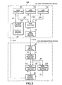
- Fig. 2 shows a characterizing portion of the data reception device 12 of the data transfer apparatus according to this embodiment.
- Fig. 2 concretely illustrated is a constitution of the information round robin section 36 to which the trouble detecting information 35 is inputted as an output side of the trouble detecting section 27 to which the output data 26 is inputted.
- Fig. 2 also concretely illustrated is a constitution of the first data processing section 311 to which a transferred data 28 is inputted.
- the second data processing section 812 has a constitution of a circuit similar to that of the first data processing section 311. As a result, illustration of the second data processing section 312 is omitted.
- the information round robin section 36 comprises first, second, and third registers 41, 42, and 43 as a serial circuit to which the trouble detecting information 35 is inputted one by one.
- An output data 44 of the first register 41 is inputted not only to the second register 42 but also to the error judging section 34.
- An output data 45 of the second register 42 is inputted not only to the third register 43 but also to the error judging section 34.
- An output data 46 of the third register 43 is inputted to the error judging section 34. Namely, the three output data 44, 45, and 46 are inputted to the error judging section 34 in parallel.
- the first data processing section 311 comprises a transferred data processing portion 47, a data effectivity information processing portion 48, and a data processor 49.
- the transferred data processing portion 47 comprises fourth, fifth, and sixth registers 51, 52, and 53 as a serial circuit to which a transferred data 281 is inputted one by one.
- An output data 54 of the fourth register 51 is inputted not only to the fifth register 52 but also to the data processor 49.
- An output data 55 of the fifth register 52 is inputted not only to the sixth register 53 but also to the data processor 49.
- An output data 66 of the sixth register 53 is inputted to the data processor 49.
- the data effectivity information processing portion 48 comprises seventh, eighth, and ninth registers 61, 62, and 63 as a serial circuit to which a data effectivity information 29 is inputted one by one.
- the data effectivity information 29 is composed of a part of the transferred data 281.
- An output data 64 of the seventh register 61 is inputted not only to the eighth register 62 but also to the data processor 49.
- An output data 65 of the eighth register 62 is inputted not only to the ninth register 63 but also to the data processor 49.
- An output data 66 of the ninth register 63 is inputted to the data processor 49. Namely, the six output data 54, 55, 56, 64, 65, and 66 are inputted to the data processor 49 in parallel.
- the general cancel information 32 outputted from the data processor 49 is inputted to the error judging section 34.
- Annulment information 69 from the error judging section 34 is inputted to the data processor 49.
- the annulment information 69 is such information for indicating an annulment of data that come to be, by re-sending, overlapping with a previously sent data among data sent from the data transmission device 11 illustrated in Fig. 1.
- respective data of one unit sent from the data transmission device 11 to the data reception device 12 is, as data of three clocks of basic clocks outputted from a clock generator (not shown), transmitted to the data transfer means 13 per each data of one clock one by one.
- the first data processing section 311 is capable of carrying out processing one by one from the time that a head data of three-divided transferred data 281 reaches.
- the second data processing section 312 illustrated in Fig. 1 is similar to the first data processing section 311. In that case, the second data processing section 312 carries out processing one by one from the time that a head data of three-divided transferred data 28 reaches.
- the trouble detecting information 35 which is outputted from the trouble detecting section 27 and which is inputted to the information round robin section 36, comprises (1) whether or not uncorrectable trouble exists, (2) an identification number indicating which the output data is outputted from, the first, the second, or the third data transmitter 141, 142, or 143, and (3) a read pointer as a reading position of any one of the first, the second, and the third data transmitters 141, 142, and 143 in the time of re-sending.
- the error judging section 34 to which the error information 37 is inputted returns, as the re-issue instruction 21, an effectivity flag, the identification number of the first, the second, or the third data transmitter 141, 142, or 143 of round robin information, and the read pointer of the corresponding the first, the second, or the third data transmitter 141, 142, or 143.
- the error judging section 34 thereby requires the re-issue from the corresponding the first, the second, or the third data transmitter 141, 142, or 143.
- the error judging section 84 issues the re-issue instruction 21 in a case that the general cancel information 32 (33) detected by the first data processing section 311 (second data processing section 312) is active.
- the re-issue control section 22 sets the read pointer of the round robin information onto the read pointer of the above-mentioned FIFO buffer.
- a decrement counter is located with being corresponding to the identification number of the first, the second, or the third data transmitter 141, 142, or 143 for which the re-issue instruction 21 becomes active.
- the decrement counter is decremented by fixed numbers of clocks to become "0".
- Figs. 3 through 5 show data transfer operations of the data transfer apparatus according to this embodiment with time base being divided into three. Besides, Figs. 3, 4, and 5 are partially overlapping with each other.
- (a) shows basic clocks 71 used in the data transfer apparatus 10. Time T1, T2,.... depicted above the basic clocks 71 show respective clock periods.
- (b) shows definers 72.
- the definers 72 show mediation timing, when the data selector 16 in the data transmission device 11 selects the output data 151, 152, or 153 outputted from the first, the second, or the third data transmitter 141, 142, or 143.
- the definers 72 become active once every three clocks of the basic clocks 71. In the example being illustrated, the definers 72 become active at the time T0, T3, T6, ...., respectively.
- FIG. 3 through 5 shows an example of a constitution of the transferred data 19 transferred by the data output section 18 illustrated in Fig. 1.
- a transferred data A shows a data transmitted by the first data transmitter 141 illustrated in Fig. 1
- a transferred data B shows a data transmitted by the second data transmitter 142 illustrated in Fig. 1.
- numbers "00" to "02" added to the respective transferred data A, B show an order of the transferred data of one unit as the precedent first half portion.
- the other numbers "10" to "12” show an order of the transferred data of one unit as the second half portion following to the precedent first half portion.
- transferred data A00D, A01D, A02D as the transferred data of the precedent one unit and transferred data A10D, A11D, A12D as the transferred data following thereto are stored in this order in the FIFO buffer of the first data transmitter 141.
- transferred data B00D, B01D, B02D as the transferred data are stored in the FIFO buffer of the second data transmitter 142.
- such an interface that the transferred data 19 outputted from the data output section 18 is received by the data input section 25 after four clocks periods of the basic clocks 71 is used as the data transfer means 13 in this embodiment.
- FIGs. 3 through 5 shows a receiving condition of the data input section 25 in the data reception device 12.
- (e), (f), (g) show storing conditions of the seventh, the eighth, the ninth registers 61, 62, 63 illustrated in Fig. 2, respectively.
- (h), (i), (j) show storing conditions of the fourth, the fifth, the sixth registers 51, 52, 53 illustrated in Fig. 2, respectively.
- (k), (l), (m) show storing conditions of the first, the second, the third registers 41, 42, 43 illustrated in Fig. 2, respectively.
- a first transferred data A00D among the data of one unit is transmitted from the data output section 18 to the data reception device 12 as the transferred data 19.
- a second transferred data A01D among the data of one unit is transmitted from the data output section 18 to the data reception device 12 as the transferred data 19.
- the definers 72 become active, and then next one unit (of three clocks of the basic clocks 71) of the output data 152 of the second data transmitter 142 is selected by the data selector 16 and decided as a selected data 17 transferred to the data output section 18.
- a third transferred data A02D among the data of one unit which has already been selected from the first data transmitter 141 is transmitted from the data output section 18 to the data reception device 12 as the transferred data 19.
- a first transferred data B00D among the data of one unit outputted from the second data transmitter 142 is transmitted from the data output section 18 to the data reception device 12 as the transferred data 19.
- a second transferred data B01D among the data of one unit is transmitted from the data output section 18 to the data reception device 12 as the transferred data 19.
- the first transferred data A00D transmitted at the time T1 from the data output section 18 is received by the data input section 25 of the data reception device 12 with a delay of four clocks periods of the basic clocks 71.
- the definers 72 become active. However, as described before, data transmitted from the third data transmitter 143 shown in Fig. 1 do not exist at this time. As a result, the output data 151 of the first data transmitter 141 is selected by the data selector 16 again. Thereby, a selected data 17 of one unit (of three clocks of the basic clocks 71) inputted to the data output section 18 is decided. At the time T6, a third transferred data B02D among the data of one unit is transmitted from the data output section 18 to the data reception device 12 as the transferred data 19. Further, at this time T6, the second transferred data A01D is received by the data input section 25 of the data reception device 12.
- the data effectivity information 29 is received by the seventh register 61.
- the first transferred data A00D is received by the fourth register 51.
- a trouble detecting information A00E for the first transferred data A00D is inputted to the first register 41 in the information round robin section 36 to which the trouble detecting information 35 is inputted. Namely, in this case, it is detected by the trouble detecting section 27 that the first transferred data A00D has the uncorrectable trouble.
- the data transfer apparatus 10 has the status that the uncorrectable trouble exists.
- the status that the uncorrectable trouble exists is shown by converting the symbol "D" indicated at an end of transferred data into the symbol "E" in this specification.
- a first transferred data A10D among the data of following one unit is transmitted from the data output section 18 to the data reception device 12 as the transferred data 19.
- the third transferred data A02D is received by the data input section 25.
- the second transferred data A01D is received by the fourth register 51 while the first transferred data A00D is received by the fifth register 52.
- a trouble detecting information A01S for the second transferred data A01D is received by the first register 41 in the information round robin section 36 to which the trouble detecting information 35 is inputted. Namely, in this case, it is not detected by the trouble detecting section 27 that the second transferred data A01D has the uncorrectable trouble.
- the data transfer apparatus 10 has the status that the uncorrectable trouble does not exist.
- the status that the uncorrectable trouble does not exist is shown by converting the symbol "D" indicated at an end of transferred data into the symbol "S" in this specification.
- a trouble detecting information A00E outputted from the first register 41 for the first transferred data A00D is received by the second register 42.
- a second transferred data A11D among the data of following one unit is transmitted from the data output section 18 to the data reception device 12 as the transferred data 19.
- the first transferred data B00D is received by the data input section 25.
- the third transferred data A02D is received by the fourth register 51 while the second transferred data A01D outputted from the fourth register 51 is received by the fifth register 52.
- the first transferred data A00D outputted from the fifth register 52 is received by the sixth register 53.
- a trouble detecting information A02S for the third transferred data A02D is received by the first register 41 in the information round robin section 36 to which the trouble detecting information 35 is inputted. Namely, in this case, it is not detected by the trouble detecting section 27 that the third transferred data A02D has the uncorrectable trouble. In this case, the data transfer apparatus 10 has the status that the uncorrectable trouble does not exist.
- a trouble detecting information A01S outputted from the first register 41 for the second transferred data A01D is received by the second register 42.
- a trouble detecting information A00E outputted from the second register 42 is received by the third register 43.
- the ninth register 63 receives the data effectivity information 29 to become active.
- the error judging section 34 is adjusted to output error information 87 on a condition that any one of the first, the second, and the third registers 41, 42, and 43 stores a status of existence of the uncorrectable trouble.
- the error judging section 34 renders the re-issue instruction 21 to be active, as illustrated in Fig. 4(n).
- the re-issue requirement signal 23 is issued from the re-issue control section 22 to the first data transmitter 141 in the data transmission device 11, as illustrated in Fig. 4 (o).
- the re-issue output data 151 from the first data transmitter 141 is indicated by a read pointer and selected by the data selector 16.
- the selected data 17 to the data output section 18 is thereby decided.
- a previously selected third transferred data A12D is transmitted from the data output section 18.
- the second transferred data B01D is received by the data input section 25.
- the data effectivity information 29 from the trouble detecting section 27 is received by the seventh register 61.
- the first transferred data B00D is received by the fourth register 51.
- the third transferred data A02D outputted from the fourth register 51 is received by the fifth register 52.
- the second transferred data A01D outputted from the fifth register 52 is received by the sixth register 53.
- a trouble detecting information B00S for the first transferred data B00D is received by the first register 41. Namely, in this case, it is not detected by the trouble detecting section 27 that the first transferred data B00D has the uncorrectable trouble. In this case, the data transfer apparatus 10 has the status that the uncorrectable trouble does not exist.
- a trouble detecting information A02S outputted from the first register 41 is received by the second register 42.
- a trouble detecting information A01S outputted from the second register 42 is received by the third register 43. Also at this time, the re-issue instruction 21 from the error judging section 34 is received by the re-issue control section 22. By the re-issue instruction 21, the annulment information 69 outputted from the error judging section 34 becomes active, as illustrated in Fig. 4 (p).
- an interval that the annulment information 69 is kept active is equal to six clocks of the basic clocks 71.
- the error judging section 34 memorizes a time for which the annulment information 69 is kept active by the numbers of clocks of the basic clocks 71 as regards the first, the second, the third data transmitters 141, 142, 143, respectively.
- the annulment information 69 is kept active in order that an information of generation of cancellation for the first half transferred data of the output data 151 outputted from the first data transmitter 141 may be held until a timing the second half of the output data 151 or the numbers of clocks of the basic clocks 71 of slip (the numbers of transaction) reaches.
- the first transferred data A00D by the re-sending is transmitted from the data output section 18.
- the third transferred data B02D is received by the data input section 25.
- an output data outputted from the seventh register 61 is received by the eighth register 62.
- the second transferred data B01D is received by the fourth register 51.
- the first outputted data B00D outputted from the fourth register 51 is received by the fifth register 52.
- the third outputted data A02D outputted from the fifth register 52 is received by the sixth register 53.
- a trouble detecting information B01S for the second transferred data B01D is received by the first register 41.
- the data transfer apparatus 10 has the status that the uncorrectable trouble does not exist.
- the first outputted data B00S outputted from the first register 41 is received by the second register 42.
- the third outputted data A02S outputted from the second register 42 is received by the third register 43.
- the annulment information 69 is kept active.
- the second transferred data A01D by the re-sending is transmitted from the data output section 18.
- the first transferred data A10D is received by the data input section 25.
- an output data outputted from the eighth register 62 is received by the ninth register 63.
- the third transferred data B02D is received by the fourth register 51.
- the outputted data B01D outputted from the fourth register 51 is received by the fifth register 52.
- the first outputted data B00D outputted from the fifth register 52 is received by the sixth register 53.
- a trouble detecting information B02S for the third transferred data B02D is received by the first register 41. In this case, it is not detected by the trouble detecting section 27 that the third transferred data B02D has the uncorrectable trouble.
- the data transfer apparatus 10 has the status that the uncorrectable trouble does not exist.
- the outputted data B01S outputted from the first register 41 is received by the second register 42.
- the outputted data B00S outputted from the second register 42 is received by the third register 43.
- the annulment information 69 is kept active.
- any one of the first, the second, and the third registers 41, 42, and 43 in the information round robin section 36 does not have the status that the uncorrectable trouble exists.
- the re-issue instruction 21 does not become active. Accordingly, as regards the data B00D, B01D, and B02D transferred from the second data transmitter 142, processing is normally completed without conducting the re-sending processing.
- the output data 151 from the first data transmitter 141 is selected by the data selector 16.
- the selected data 17 to the data output section 18 is thereby decided.
- the third transferred data A02D is transmitted from the data output section 18.
- the second transferred data A11D is received by the data input section 25.
- the data effectivity information 29 is received by the seventh register 61.
- the first transferred data A10D is received by the fourth register 51.
- the output data B02D outputted from the fourth register 51 is received by the fifth register 52.
- the output data B01D outputted from the fifth register 52 is received by the sixth register 53.
- a trouble detecting information A10S for the first transferred data A10D is received by the first register 41.
- the data transfer apparatus 10 has the status that the uncorrectable trouble does not exist.
- the output data B02S outputted from the first register 41 is received by the second register 42.
- the output data B01S outputted from the second register 42 is received by the third register 43.
- the annulment information 69 is kept active.
- the first transferred data A10D as a following transmitted data is transmitted from the data output section 18.
- the third transferred data A12D is received by the data input section 25.
- an output data outputted from the seventh register 61 is received by the eighth register 62.
- the second transferred data A11D is received by the fourth register 51.
- the output data A10D outputted from the fourth register 51 is received by the fifth register 62.
- the output data B02D outputted from the fifth register 52 is received by the sixth register 53.
- a trouble detecting information A11S for the second transferred data A11D is received by the first register 41. In this case, it is not detected by the trouble detecting section 27 that the second transferred data A11D has the uncorrectable trouble.
- the data transfer apparatus 10 has the status that the uncorrectable trouble does not exist.
- the output data A10S outputted from the first register 41 is received by the second register 42.
- the output data B02S outputted from the second register 42 is received by the third register 43.
- the annulment information 69 is kept active.
- the second transferred data A11D is transmitted from the data output section 18.
- the first transferred data A00D is received by the data input section 25.
- an output data outputted from the eighth register 62 is received by the ninth register 63.
- the third transferred data A12D is received by the fourth register 51.
- the output data A11D outputted from the fourth register 51 is received by the fifth register 52.
- the output data A10D outputted from the fifth register 52 is received by the sixth register 53.
- a trouble detecting information A12S for the third transferred data A12D is received by the first register 41. In this case, it is not detected by the trouble detecting section 27 that the third transferred data A12D has the uncorrectable trouble.
- the data transfer apparatus 10 has the status that the uncorrectable trouble does not exist.
- the output data A11S outputted from the first register 41 is received by the second register 42.
- the output data A10S outputted from the second register 42 is received by the third register 43.
- the annulment information 69 is kept active.
- the annulment information 69 makes the data effectivity information of the ninth register 63 be invalid. Namely, the transferred data A10D, A11D, and A12D are completed without conducting processing.
- a previous processing may be conducted, when the seventh register 61 and the eighth register 62 are active. However, when the ninth register 63 of the last stage is active, all processing are rendered to be invalid.
- the third transferred data A12D is transmitted from the data output section 18.
- the second transferred data A01D is received by the data input section 25.
- the data effectivity information 29 is received by the seventh register 61.
- the first transferred data A00D is received by the fourth regieter 51.
- the third output data A12D outputted from the fourth register 51 is received by the fifth register 52.
- the second output data A11D outputted from the fifth register 52 is received by the sixth register 53.
- a trouble detecting information A00S for the first transferred data A00D is received by the first register 41. In this case, it is not detected by the trouble detecting section 27 that the first transferred data A00D has the uncorrectable trouble.
- the data transfer apparatus 10 has the status that the uncorrectable trouble does not exist.
- the output data A12S outputted from the first register 41 is received by the second register 42.
- the output data A11S outputted from the second register 42 is received by the third register 43.
- the annulment information 69 inputted to the data processor 49 becomes inactive from this time.
- the third transferred data A02D is received by the data input section 25. Further, an output data outputted from the seventh register 61 is received by the eighth register 62.
- the second transferred data A01D is received by the fourth register 51.
- the first output data A00D outputted from the fourth register 51 is received by the fifth register 52.
- the third output data A12D outputted from the fifth register 52 is received by the sixth register 53.
- a trouble detecting information A01S for the second transferred data A01D is received by the first register 41. In this case, it is not detected by the trouble detecting section 27 that the second transferred data A01D has the uncorrectable trouble. In this case, the data transfer apparatus 10 has the status that the uncorrectable trouble does not exist.
- the output data A00S outputted from the first register 41 is received by the second register 42.
- the output data A12S outputted from the second register 42 is received by the third register 43.
- the first transferred data A10D is received by the data input section 25. Further, an output data outputted from the eighth register 62 is received by the ninth register 63.
- the third transferred data A02D is received by the fourth register 51.
- the second output data A01D outputted from the fourth register 51 is received by the fifth register 52.
- the first output data A00D outputted from the fifth register 52 is received by the sixth register 53.
- a trouble detecting information A02S for the third transferred data A02D is received by the first register 41. In this case, it is not detected by the trouble detecting section 27 that the third transferred data A02D has the uncorrectable trouble. In this case, the data transfer apparatus 10 has the status that the uncorrectable trouble does not exist.
- the output data A01S outputted from the first register 41 is received by the second register 42.
- the output data A00S outputted from the second register 42 is received by the third register 43.
- the ninth register 63 is active, any one of the first, the second, and the third registers 41, 42, and 43 in the information round robin section 36 does not have the status that the uncorrectable trouble exists.
- the re-issue instruction 21 does not become active. Accordingly, as regards the data A00D, A01D, and A02D transferred from the first data transmitter 141, processing is normally completed.
- processing is conducted by the steps similar to the above.
- the data transfer apparatus 10 comprises means for re-sending those data A10D, A11D, and A12D and annulling the re-sent data A10D, A11D, and A12D thereafter.
- coexistence with the general cancellation function is available. It is not at all necessary that hardware for exclusive use of re-sending is prepared. Thereby, reduction of cost can be achieved in this embodiment.
- the data transfer apparatus 10 has the information round robin section 36, so that the trouble detecting information 35 obtained by detection of the trouble detecting section 27 is taken around.
- the information round robin section 36 takes the identification numbers of the data transmitters 141 to 143, and read pointers of the data transmitters 141 to 143 around.
- the embodiment has a little possibility that data transfer incapable of being relieved is generated. Namely, in a case that an uncorrectable trouble exists in the first transferred data, the data transfer apparatus brings about a system down.
- Such a problem can be solved by providing a circuit corresponding to the information round robin section 36 in the first embodiment at the side of the data transmission device 11. This will be hereunder described as a second embodiment of the present invention.
- Fig. 6 schematically shows a constitution of a data transfer apparatus according to a second embodiment of the present invention.
- a re-issue control section 22A in a data transmission device 11A comprises a buffer memory 81.
- a data reception device 12A does not have the information round robin section 36 (in Fig. 1). A role of the information round robin section 36 is conducted by the buffer memory 81.
- the identification numbers of the data transmitters 141 to 143 and the read pointers of the data transmitters 141 to 143 each of which is corresponding to a transferred data issued from the data transmitter 141, 142, or 143 are registered in the buffer memory 81 of the re-issue control section 22A one by one.
- a re-issue instruction 21A having no additional information for the read pointers of the data transmitters 141 to 143, and the like is returned from the error judging section 34.
- the number of clocks of the basic clocks 71 (shown in Fig. 3) until a transferred data reaches the error judging section 34 after the transferred data is issued from the data output section 18 is a fixed number. Therefore, in a case that a re-issue instruction 21A is not generated at the timing for generating the re-issue instruction 21A, it is decided that the re-issue does not need to be conducted. Namely, the data transfer apparatus 10A makes the identification numbers of the data transmitters 141 to 143 and the read pointers of the data transmitters 141 to 143 both of which are registered in the buffer memory 81 of the re-issue control section 22A be invalid.
- the data transfer is conducted in a three-divided manner.
- the number of division is not restricted to three.
- the number of division may be any numbers, as far as the number is a positive integer.
- a reaching time of the transferred data 19 from the data transmission device 11 to the data reception device 12 is equal to four clocks of the basic clocks 71.
- the number of the clocks may be any numbers, as far as the number is a positive integer.
- the data transmitter is composed of three data transmitters 141, 142, and 143.
- the number of the data transmitter is not restricted to three.
- these data transmitters 141, 142, and 143 are composed of FIFO memories.
- the data transmitters 141, 142, and 143 are not restricted to such FIFO memories.
- a constitution similar to the FIFO memories may be alternatively obtained by conducting a control for protecting an order of transferring data using an arithmetic processing unit, such as a microprocessor, and the like.
- the data processing section can, of course, be composed of any numbers of the data processing sections.
- the data processing section may be composed of a memorizing device, and the like for storing data.
- an order of transferring data is guaranteed in the same data transmitter 141, 142, or 143 among the first to the third data transmitters 141 to 143.
- This is not restricted to the above.
- it is not necessary to re-issue the data after receiving the re-issue instruction 21 with being entangled therein by a re-set of an effective flag within the first, the second and the third data transmitters 141, 142 and 143 as regards the data having already been issued.
- data transfer means 13 as an interface is rendered to have one to one connection between the data transmission device 11 and the data reception device 12.
- a plurality of data transmission devices and a plurality of data reception devices may be connected to the data transfer means 13 by using a bus connection, or the like.
- a data transmitter of a data transmission source can be identified by taking the numbers of the data transmission devices of a data transmission source around in addition to the identification numbers of the data transmitters 141, 142, 143 and the read pointers of the data transmitters 141, 142, 143.
- definers are used for the mediation timings in the data selector 16.
- the mediations are conducted at any timings and acknowledges from the data output section 18 are waited therefor.
- the data output section 18 and the data input section 25 are composed of registers.
- the data output section 18 and the data input section 25 may be composed of the other circuit devices, such as buffers, and the like.
- the uncorrectable troubles are repeated, re-issues of the data are also repeated.
- a check of the system itself may be conducted as a disorder or a trouble each incapable of being restored at the present time.
- ECC control circuits are used for detecting the uncorrectable troubles. Any detecting means, such as a parity check, and the like can also be used.
- the data transfer apparatus has a plurality of data storing means for storing data of which transmission timing must not be influenced by delay of transmission timing of the other data at least with the data being stored separately to each other, and data selecting means for selecting data per one unit one by one at predetermined frequency and order with respect to said a plurality of data storing means, respectively.
- data to be re-sent is read out and is transmitted.
- a circuit can be commonly used. It is not at all necessary that hardware for exclusive use of re-sending is prepared. Thereby, reduction of cost can be achieved in the data transfer apparatus.
Landscapes
- Engineering & Computer Science (AREA)
- Multimedia (AREA)
- Computer Networks & Wireless Communication (AREA)
- Signal Processing (AREA)
- Detection And Prevention Of Errors In Transmission (AREA)
- Time-Division Multiplex Systems (AREA)
Applications Claiming Priority (2)
| Application Number | Priority Date | Filing Date | Title |
|---|---|---|---|
| JP2002147195A JP3741077B2 (ja) | 2002-05-22 | 2002-05-22 | データ転送装置 |
| JP2002147195 | 2002-05-22 |
Publications (1)
| Publication Number | Publication Date |
|---|---|
| EP1365535A2 true EP1365535A2 (de) | 2003-11-26 |
Family
ID=29397847
Family Applications (1)
| Application Number | Title | Priority Date | Filing Date |
|---|---|---|---|
| EP03011635A Withdrawn EP1365535A2 (de) | 2002-05-22 | 2003-05-22 | Datenübertragungsvorrichtung mit Sendewiederholungen |
Country Status (3)
| Country | Link |
|---|---|
| US (1) | US7039729B2 (de) |
| EP (1) | EP1365535A2 (de) |
| JP (1) | JP3741077B2 (de) |
Cited By (1)
| Publication number | Priority date | Publication date | Assignee | Title |
|---|---|---|---|---|
| US8742782B2 (en) | 2011-07-27 | 2014-06-03 | International Business Machines Corporation | Noncontact electrical testing with optical techniques |
Family Cites Families (12)
| Publication number | Priority date | Publication date | Assignee | Title |
|---|---|---|---|---|
| US4051355A (en) * | 1976-04-29 | 1977-09-27 | Ncr Corporation | Apparatus and method for increasing the efficiency of random access storage |
| US4070648A (en) * | 1976-06-18 | 1978-01-24 | Ncr Corporation | Computer to computer communication system |
| JPS6468145A (en) * | 1987-09-09 | 1989-03-14 | Matsushita Electric Industrial Co Ltd | Data transmission equipment |
| US5271020A (en) * | 1990-12-21 | 1993-12-14 | Intel Corporation | Bus stretching protocol for handling invalid data |
| US5191649A (en) * | 1990-12-21 | 1993-03-02 | Intel Corporation | Multiprocessor computer system with data bus and ordered and out-of-order split data transactions |
| US5933623A (en) * | 1995-10-26 | 1999-08-03 | Hitachi, Ltd. | Synchronous data transfer system |
| JPH10247901A (ja) * | 1997-03-04 | 1998-09-14 | Matsushita Electric Ind Co Ltd | 再送制御方法 |
| US6118769A (en) * | 1997-05-01 | 2000-09-12 | Itt Manufacturing Enterprises, Inc. | Method and apparatus for voice intranet repeater and range extension |
| US6366979B1 (en) * | 1997-12-16 | 2002-04-02 | Cypress Semiconductor Corp. | Apparatus and method for shorting retransmit recovery times utilizing cache memory in high speed FIFO |
| JP2000244530A (ja) * | 1999-02-23 | 2000-09-08 | Fuji Xerox Co Ltd | データ通信装置 |
| US6643752B1 (en) * | 1999-12-09 | 2003-11-04 | Rambus Inc. | Transceiver with latency alignment circuitry |
| JP4033615B2 (ja) * | 2000-09-01 | 2008-01-16 | 株式会社ケンウッド | 無線データ伝送における誤り制御方式 |
-
2002
- 2002-05-22 JP JP2002147195A patent/JP3741077B2/ja not_active Expired - Fee Related
-
2003
- 2003-05-22 EP EP03011635A patent/EP1365535A2/de not_active Withdrawn
- 2003-05-22 US US10/443,941 patent/US7039729B2/en not_active Expired - Fee Related
Cited By (1)
| Publication number | Priority date | Publication date | Assignee | Title |
|---|---|---|---|---|
| US8742782B2 (en) | 2011-07-27 | 2014-06-03 | International Business Machines Corporation | Noncontact electrical testing with optical techniques |
Also Published As
| Publication number | Publication date |
|---|---|
| US7039729B2 (en) | 2006-05-02 |
| JP3741077B2 (ja) | 2006-02-01 |
| JP2003338808A (ja) | 2003-11-28 |
| US20030221154A1 (en) | 2003-11-27 |
Similar Documents
| Publication | Publication Date | Title |
|---|---|---|
| US6718444B1 (en) | Read-modify-write for partial writes in a memory controller | |
| EP0503545B1 (de) | Einrichtung zur Datenübertragung | |
| US4489379A (en) | Distributed data processing in ring-structured networks architected for full duplex peer-to-peer operation of processing stations and uninterruptible transfer of long data records between stations | |
| KR100308719B1 (ko) | 통신 수신기에서 흐름 제어 및 라우팅을 개선한 다중 에프아이에프오를 사용하기 위한 방법 및 장치 | |
| EP0029331A1 (de) | System zur Übertragung zwischen Untersystemen | |
| US8107377B2 (en) | Reordering packets | |
| US7821919B2 (en) | Data processing apparatus and data processing method | |
| US8966354B2 (en) | Communication system via cascade connection and communication device | |
| US7200790B2 (en) | Switch level reliable transmission | |
| US6543014B1 (en) | Data transmitting/receiving apparatus for executing data retransmission and parallel processor system | |
| US6263393B1 (en) | Bus switch for realizing bus transactions across two or more buses | |
| US7039729B2 (en) | Data transfer apparatus | |
| EP0242634A2 (de) | Bytezählergebnisbehandlung in einer seriellen Kanalerweiterung mit Pufferung von vorausgeholten Daten | |
| EP2571187A1 (de) | Informationsverarbeitungssystem, Übertragungsvorrichtung, Empfangsvorrichtung und Verfahren zum Verarbeiten von Informationen | |
| KR0174853B1 (ko) | 상대방 메모리를 이용한 두 프로세서간 비동기 직렬 통신 송/수신 장치 | |
| US5331647A (en) | Communication apparatus having function to record communication history | |
| JP2692773B2 (ja) | エラー訂正装置 | |
| US5590279A (en) | Memory data copying apparatus | |
| US5592680A (en) | Abnormal packet processing system | |
| JPS61103298A (ja) | 複写機制御装置 | |
| JP6273664B2 (ja) | データ送信装置、およびデータ送信方法 | |
| JP5093986B2 (ja) | プロセッサ間通信方法及びプロセッサ間通信装置 | |
| JP2007103999A (ja) | データ転送制御装置、およびデータ転送制御方法 | |
| JP4239482B2 (ja) | データ転送システム、lsi及びデータ転送方法 | |
| JP2000115258A (ja) | 通信エラー自動修復システム |
Legal Events
| Date | Code | Title | Description |
|---|---|---|---|
| PUAI | Public reference made under article 153(3) epc to a published international application that has entered the european phase |
Free format text: ORIGINAL CODE: 0009012 |
|
| AK | Designated contracting states |
Kind code of ref document: A2 Designated state(s): AT BE BG CH CY CZ DE DK EE ES FI FR GB GR HU IE IT LI LU MC NL PT RO SE SI SK TR |
|
| AX | Request for extension of the european patent |
Extension state: AL LT LV MK |
|
| STAA | Information on the status of an ep patent application or granted ep patent |
Free format text: STATUS: THE APPLICATION HAS BEEN WITHDRAWN |
|
| 18W | Application withdrawn |
Effective date: 20061109 |