EP1365327B1 - Ein Verfahren und Netzwerkvorrichtung bestehend aus einem flexiblem EEPROM um Konfigurationseinstellungen einzustellen - Google Patents
Ein Verfahren und Netzwerkvorrichtung bestehend aus einem flexiblem EEPROM um Konfigurationseinstellungen einzustellen Download PDFInfo
- Publication number
- EP1365327B1 EP1365327B1 EP03010477A EP03010477A EP1365327B1 EP 1365327 B1 EP1365327 B1 EP 1365327B1 EP 03010477 A EP03010477 A EP 03010477A EP 03010477 A EP03010477 A EP 03010477A EP 1365327 B1 EP1365327 B1 EP 1365327B1
- Authority
- EP
- European Patent Office
- Prior art keywords
- network device
- default values
- memory
- interface
- updated
- Prior art date
- Legal status (The legal status is an assumption and is not a legal conclusion. Google has not performed a legal analysis and makes no representation as to the accuracy of the status listed.)
- Expired - Lifetime
Links
Images

Classifications
-
- G—PHYSICS
- G06—COMPUTING OR CALCULATING; COUNTING
- G06F—ELECTRIC DIGITAL DATA PROCESSING
- G06F9/00—Arrangements for program control, e.g. control units
- G06F9/06—Arrangements for program control, e.g. control units using stored programs, i.e. using an internal store of processing equipment to receive or retain programs
- G06F9/44—Arrangements for executing specific programs
- G06F9/4401—Bootstrapping
- G06F9/4411—Configuring for operating with peripheral devices; Loading of device drivers
-
- G—PHYSICS
- G06—COMPUTING OR CALCULATING; COUNTING
- G06F—ELECTRIC DIGITAL DATA PROCESSING
- G06F13/00—Interconnection of, or transfer of information or other signals between, memories, input/output devices or central processing units
- G06F13/10—Program control for peripheral devices
-
- G—PHYSICS
- G06—COMPUTING OR CALCULATING; COUNTING
- G06F—ELECTRIC DIGITAL DATA PROCESSING
- G06F13/00—Interconnection of, or transfer of information or other signals between, memories, input/output devices or central processing units
- G06F13/14—Handling requests for interconnection or transfer
-
- G—PHYSICS
- G06—COMPUTING OR CALCULATING; COUNTING
- G06F—ELECTRIC DIGITAL DATA PROCESSING
- G06F13/00—Interconnection of, or transfer of information or other signals between, memories, input/output devices or central processing units
- G06F13/38—Information transfer, e.g. on bus
-
- G—PHYSICS
- G06—COMPUTING OR CALCULATING; COUNTING
- G06F—ELECTRIC DIGITAL DATA PROCESSING
- G06F13/00—Interconnection of, or transfer of information or other signals between, memories, input/output devices or central processing units
- G06F13/38—Information transfer, e.g. on bus
- G06F13/40—Bus structure
- G06F13/4004—Coupling between buses
- G06F13/4022—Coupling between buses using switching circuits, e.g. switching matrix, connection or expansion network
-
- G—PHYSICS
- G06—COMPUTING OR CALCULATING; COUNTING
- G06F—ELECTRIC DIGITAL DATA PROCESSING
- G06F15/00—Digital computers in general; Data processing equipment in general
- G06F15/16—Combinations of two or more digital computers each having at least an arithmetic unit, a program unit and a register, e.g. for a simultaneous processing of several programs
- G06F15/177—Initialisation or configuration control
-
- G—PHYSICS
- G06—COMPUTING OR CALCULATING; COUNTING
- G06F—ELECTRIC DIGITAL DATA PROCESSING
- G06F17/00—Digital computing or data processing equipment or methods, specially adapted for specific functions
-
- G—PHYSICS
- G06—COMPUTING OR CALCULATING; COUNTING
- G06F—ELECTRIC DIGITAL DATA PROCESSING
- G06F3/00—Input arrangements for transferring data to be processed into a form capable of being handled by the computer; Output arrangements for transferring data from processing unit to output unit, e.g. interface arrangements
-
- H—ELECTRICITY
- H04—ELECTRIC COMMUNICATION TECHNIQUE
- H04L—TRANSMISSION OF DIGITAL INFORMATION, e.g. TELEGRAPHIC COMMUNICATION
- H04L41/00—Arrangements for maintenance, administration or management of data switching networks, e.g. of packet switching networks
- H04L41/08—Configuration management of networks or network elements
- H04L41/0803—Configuration setting
- H04L41/0813—Configuration setting characterised by the conditions triggering a change of settings
- H04L41/082—Configuration setting characterised by the conditions triggering a change of settings the condition being updates or upgrades of network functionality
-
- H—ELECTRICITY
- H04—ELECTRIC COMMUNICATION TECHNIQUE
- H04L—TRANSMISSION OF DIGITAL INFORMATION, e.g. TELEGRAPHIC COMMUNICATION
- H04L69/00—Network arrangements, protocols or services independent of the application payload and not provided for in the other groups of this subclass
- H04L69/12—Protocol engines
-
- H—ELECTRICITY
- H04—ELECTRIC COMMUNICATION TECHNIQUE
- H04L—TRANSMISSION OF DIGITAL INFORMATION, e.g. TELEGRAPHIC COMMUNICATION
- H04L69/00—Network arrangements, protocols or services independent of the application payload and not provided for in the other groups of this subclass
- H04L69/22—Parsing or analysis of headers
Definitions
- the present invention relates to a network device having an apparatus for selectively configuring the network device using an Electrically Erasable Programmable Read Only Memory (EEPROM). More specifically, the network device is able to use dynamic configuration settings in the EEPROM interface, that increases flexibility, has fewer limitations and is a low cost alternative.
- EEPROM Electrically Erasable Programmable Read Only Memory
- Network devices are necessary to allow a network to function properly. These network devices are composed of chips, with these chips allowing for the control and monitoring of data through the network device. Chip vendors may pre-set some register default values inside a network device, such as a switch/hub chip, to provide a low cost switch and hub application. That means it is not necessary for system integrators to change the internal register default values to build a workable system. The preconfigured chips allow for the network devices to be setup and to function quickly for a majority of system integrators.
- these pre-set register default values might not suitable for some system integrators.
- Chip vendors should provide some methods so that system integrators can change some register values instead of using default values.
- Some chip vendors will provide a microprocessor interface (SPI, I2C, or PCI) to allow system integrators to change all write-able registers.
- SPI microprocessor interface
- I2C I2C
- PCI microprocessor interface
- EEPROM Electrically Erasable Programmable Read Only Memory
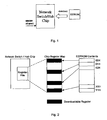
- Fig. 1 provides as an example of a low cost pre-programmed EEPROM that is used to change some default values of a network switch/hub chip.
- RESET external control signal
- network switch/hub chip start to change its some register default values via downloading the contents of EEPROM. And then network switch/hub chip start its normal operation after the download phase had been finished.
- the network switch/hub chip When the RESET signal goes to inactive, the network switch/hub chip starts to fetch data from external EEPROM automatically. Most of the network switch/hub chips will fetch data from EEPROM address 00h (the first entry), and fetch the other data in sequence. In order to change some register default values or set chip configuration, the chip vendor will provide a register set (a part of chip register file) which are downloadable from EEPROM. Each entry of EEPROM is pre-defined and will directly map to one or more entries of a register set inside network switch/hub chip as described in Fig. 2.
- the present invention provides for a new approach for chip and network component vendors to provide system integrators a dynamic configuration using a low cost EEPROM.
- system integrators will have flexibility to change the default values of all configurable registers inside a network device, such as a switch/hub chip or components on a PC board.
- a network device will be able to update configuration setting either through the low cost EEPROM or though a microprocessor interface.
- the present invention is directed to changing the contents of the EEPROM used in a network device to a set of configuration instructions instead of configuration values only.
- Each configuration instruction can be composed of address index and its corresponding desired value.
- An indirect mapping mechanism is used to map EEPROM contents to their corresponding registers inside network switch/hub chip instead of original direct mapping method.
- a header, encapsulated with a specific key value and total number of configuration instructions, should be filled in the first entry of EEPROM content. This header is designed as an identifier during EEPROM download cycle.
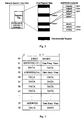
- Fig. 3 One embodiment of the present invention is illustrated in Fig. 3.
- the network device inclusive of such a switch/hub chip, should have a built-in circuit (called, in this example, Configuration Instruction Interpreter, CII) inside the chip to interpret configuration instruction.
- CII Configuration Instruction Interpreter
- RESET signal goes to inactive
- the CII of network switch/hub chip start to fetch header (the first entry) from external EEPROM automatically, then the key is obtained. If the key value is not matched with the number pre-defined inside network device, it indicates that it is not necessary to change any chip default value, and download sequence might be skipped.
- the CII continuously fetches configuration instruction from EEPROM, and changes the corresponding (defined in address index of configuration instruction) register default value to the desired value by interpreting instruction. This process will be repeated until all instruction download completely. Additionally, since the number of default values needing to be updated is determined from the start, the time needed to perform the updated is less than the equivalent updating performed in the prior art methods and systems.
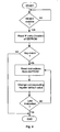
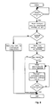
- Fig. 4 This process, described above, is illustrated in Fig. 4.
- the process continually checks to see if the RESET signal is set to inactive. Once the RESET signal is inactive, the header of the EEPROM is read. A key is determined and compared with the pre-defined number inside the chip. If there is a match, then instructions are read from the EEPROM and the corresponding register default value is changed. If the immediately previous instruction just read was the last, then, in this example, the process ends. If that previous instruction was not the last, then the next instruction is read from the EEPROM and the default values of the corresponding register are changed.
- a system integrator could use a very cost EEPROM to change any downloadable register default value.
- the system integrator could decide which registers he wants to change the default values without too much limitation. Additionally, the system integrator also could decide how many registers he wants to change. Such that, less capacity EEPROM could be used due to few register default values changed.
- the EEPROM system and method discussed above increases the versatility of the network devices, as compared to such devices without an EEPROM interface.
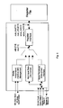
- a portion of a network device without such an EEPROM interface is schematically illustrated in Fig. 5.
- the network device of this example is a low-cost switch that can be used to perform high-speed switching, including packet buffers, transceivers, media access controllers, address management and non-blocking switch controller.
- Other configurations are possible and the present invention is not limited to the network device illustrated in Fig. 5. Since the network device is designed for cost sensitive unmanaged markets and requires only a low cost micro controller to initialize and configure the device, the use of above-described EEPROM to set configuration settings is particularly attractive.
- the portions of such a network switch illustrated in Fig. 5 include a Media-Independent Interface (MII) management section and a Serial Peripheral Interconnect (SPI) Interface section.
- MII Media-Independent Interface
- SPI Serial Peripheral Interconnect
- the device sends and receives data through these interfaces and communicates with the register interface, to read and write to a register file.
- MII Media-Independent Interface
- SPI Serial Peripheral Interconnect
- the device can have an EEPROM interface. Portions of such a network device are illustrated in Fig. 6. This allows for the device to update the default values of the network device using either the EEPROM interface or SPI interface.
- the network switch cannot co-exist in both the EEPROM and SPI modes. The single mode operation does not require the resolution of conflicting instructions to the register file that can occur if both modes were operational.
- the first entry in the EEPROM contains a key that determines the operation of the EEPROM.
- the first entry also contains a speed select bit and provides a total number of entries in the EEPROM.
- an address number is provided with a specific number provided for a change page and other numbers representing an offset address.
- the data entry number can be, in this example, one of four numbers: 1 for an 8-/16-bit value, 2 for a 24-/32-bit value, 3 for a 40-/48-bit value and 4 for a 56-/64-bit value, with the last being a maximum. Data follows each address tag.
- the network device does not co-exist in both the EEPROM and the microprocessor modes.
- the first thing to be determined is which mode is applied to this network device after the RESET signal goes to inactive. It is necessary to have another control pin (that can be called a STRAP pin) to indicate which configuration mode is selected. This process is illustrated in Fig. 8.
- the network device checks to determine if the RESET signal has been set to inactive. If it has, then a control pin is read to determine if either the EEPROM interface or the SPI interface is selected. If the control pin indicates that the SPI interface is selected, then the network device waits for a microprocessor to configure the registers over the SPI interface. Otherwise, if the EEPROM interface is selected, then the rest of the process steps are carried out. These steps are similar to those illustrated in Fig. 4 and their description need not be repeated.
- the network chip When the EEPROM mode is selected, the network chip is a MASTER and external EEPROM is a SLAVE. That is all control signals are driven from chip to EEPROM. In such a mode, all registers in the network device are configurable.
- the network device When microprocessor mode is selected, the network device is a SLAVE and the external microprocessor is a MASTER. That is, all control signals are driven from microprocessor to chip. All registers in the network device are configurable and read-able.
- the network device embodying the present invention would have numerous benefits over the prior art devices.
- the network device allows for a system integrator to make changes to default settings of the network device that is not costly or cumbersome. Additionally, only certain defaults on a network device may be changed without the limitations imposed by the prior art processes and devices. Also, the network device allows for the use of multiple inputs to allow for changes to the default values of the network device.
- One configuration of the invention is, in one embodiment, embodied on a semiconductor substrate, such as silicon, with appropriate semiconductor manufacturing techniques and based upon a circuit layout which would, based upon the embodiments discussed above, be apparent to those skilled in the art.
- a person of skill in the art with respect to semiconductor design and manufacturing would be able to implement the various modules, interfaces, and components, etc. of the present invention onto a single semiconductor substrate, based upon the architectural description discussed above. It would also be within the scope of the invention to implement the disclosed elements of the invention in discrete electronic components, thereby taking advantage of the functional aspects of the invention without maximizing the advantages through the use of a single semiconductor substrate.
Landscapes
- Engineering & Computer Science (AREA)
- Theoretical Computer Science (AREA)
- Physics & Mathematics (AREA)
- General Engineering & Computer Science (AREA)
- General Physics & Mathematics (AREA)
- Software Systems (AREA)
- Computer Networks & Wireless Communication (AREA)
- Computer Security & Cryptography (AREA)
- Computer Hardware Design (AREA)
- Signal Processing (AREA)
- Mathematical Physics (AREA)
- Data Mining & Analysis (AREA)
- Databases & Information Systems (AREA)
- Human Computer Interaction (AREA)
- Stored Programmes (AREA)
- Small-Scale Networks (AREA)
- Multi Processors (AREA)
Claims (13)
- Verfahren zum Konfigurieren von Voreinstellungswerten einer Netzwerkeinrichtung, wobei die Netzwerkeinrichtung in einem Mikroprozessor-Modus oder in einem Speicher-Modus vorliegt, wobei das Verfahren die folgenden Verfahrensschritte aufweist:a) Bestimmen, ob die Voreinstellungswerte über eine Mikroprozessor-Schnittstelle oder eine Speicher-Schnittstelle erhalten werden, wobei die Mikroprozessor-Schnittstelle und die Speicher-Schnittstelle gemeinsam die gleichen Sockelstifte nutzen;b) wenn bestimmt wird, dass die Voreinstellungswerte über die Speicher-Schnittstelle erhalten werden: Ausführen der folgenden Verfahrensschritte:b1) Empfangen einer Kopfzeile von einem Speicher über die Speicher-Schnittstelle;b2) Bestimmen von der Kopfzeile, ob irgendein Voreinstellungswert der Netzwerkeinrichtung aktualisiert werden muss;b3) Abrufen von zumindest einer Konfigurationsanweisung von dem Speicher, wenn beim Verfahrensschritt des Bestimmens bestimmt wird, dass die Netzwerkeinrichtung aktualisiert werden muss;b4) Interpretieren der zumindest einen Konfigurationsanweisung; undb5) Ändern eines Register-Voreinstellungswertes der Voreinstellungswerte entsprechend der interpretierten, zumindest einen Konfigurationsanweisung; undc) wenn bestimmt wird, dass die Voreinstellungswerte über die Mikroprozessor-Schnittstelle erhalten werden: Ändern der Voreinstellungswerte gemäß Daten, die über die Mikroprozessor-Schnittstelle empfangen werden.
- Verfahren nach Anspruch 1, wobei das Verfahren ferner den Verfahrensschritt des Überwachens eines Rücksetzsignals aufweist, um zu bestimmen, ob die Voreinstellungswerte der Netzwerkeinrichtung aktualisiert werden müssen.
- Verfahren nach Anspruch 1, wobei der Verfahrensschritt b2) den Verfahrensschritt des Bestimmens einer Anzahl der Voreinstellungswerte der Netzwerkeinrichtung, die aktualisiert werden müssen, von der Kopfzeile aufweist.
- Verfahren nach Anspruch 3, wobei der Verfahrensschritt b3) den Verfahrensschritt des Abrufens einer Anzahl von Konfigurationsanweisungen von dem Speicher aufweist, die gleich der Anzahl der Voreinstellungswerte der Netzwerkeinrichtung ist, welche aktualisiert werden müssen.
- Verfahren nach Anspruch 1, wobei der Verfahrensschritt b2) den Verfahrensschritt des Bestimmens eines Schlüsselwertes von der Kopfzeile und den Verfahrensschritt des Vergleichens des Schlüsselwertes mit einer zuvor innerhalb der Netzwerkeinrichtung festgelegten Nummer aufweist, um zu bestimmen, ob irgendein Voreinstellungswert der Netzwerkeinrichtung aktualisiert werden muss.
- Verfahren nach Anspruch 1, wobei die zumindest eine Konfigurationsanweisung eine Vielzahl von Konfigurationsanweisungen aufweist, und wobei der Verfahrensschritt b3) so lange wiederholt wird, bis alle Konfigurationsanweisungen der Vielzahl der Konfigurationsanweisungen abgerufen wurden.
- Netzwerkeinrichtung, welche in einem Mikroprozessor-Modus oder in einem Speicher-Modus vorliegt, wobei die Netzwerkeinrichtung folgendes aufweist:- eine Einrichtung zum Bestimmen, ob die Voreinstellungswerte über eine Mikroprozessor-Schnittstelle oder eine Speicher-Schnittstelle erhalten werden, wobei die Mikroprozessor-Schnittstelle und die Speicher-Schnittstelle die gleichen Sockelstifte nutzen;- eine Einrichtung zum Empfangen einer Kopfzeile von einem Speicher über die Speicher-Schnittstelle;- eine Einrichtung zum Bestimmen von der Kopfzeile, ob irgendein Voreinstellungswert der Netzwerkeinrichtung aktualisiert werden muss;- eine Einrichtung zum Abrufen von zumindest einer Konfigurationsanweisung von dem Speicher, wenn der Verfahrensschritt des Bestimmens zeigt, dass die Netzwerkeinrichtung aktualisiert werden muss;- eine Einrichtung zum Interpretieren von der zumindest einen Konfigurationsanweisung;- eine Einrichtung, welche einen Register-Voreinstellungswert der Voreinstellungswerte entsprechend der interpretierten, zumindest einen Konfigurationsanweisung ändert; und- eine Einrichtung zum Ändern der Voreinstellungswerte gemäß Daten, die über die Mikroprozessor-Schnittstelle empfangen werden; wobei die Einrichtung zum Ändern der Voreinstellungswerte gemäß den durch die Mikroprozessor-Schnittstelle empfangenen Daten derart konfiguriert ist, um die Voreinstellungswerte zu ändern, wenn die Einrichtung zum Bestimmen, ob die Voreinstellungswerte über eine Mikroprozessor-Schnittstelle oder über eine Speicher-Schnittstelle erhalten werden, bestimmt, dass die Voreinstellungswerte über eine Mikroprozessor-Schnittstelle erhalten werden müssen.
- Netzwerkeinrichtung nach Anspruch 7, welche ferner eine Einrichtung zum Überwachen eines Rücksetzsignals aufweist, um zu bestimmen, ob die Voreinstellungswerte der Netzwerkeinrichtung aktualisiert werden müssen.
- Netzwerkeinrichtung nach Anspruch 7, wobei die Einrichtung zum Bestimmen von der Kopfzeile, ob irgendein Voreinstellungswert der Netzwerkeinrichtung aktualisiert werden muss, eine Einrichtung zum Bestimmen einer Anzahl der Voreinstellungswerte der Netzwerkeinrichtung von der Kopfzeile aufweist, die aktualisiert werden müssen.
- Netzwerkeinrichtung nach Anspruch 9, wobei die Einrichtung zum Abrufen von der zumindest einen Konfigurationsanweisung von dem Speicher eine Einrichtung zum Abrufen einer Anzahl von Konfigurationsanweisungen von dem Speicher aufweist, die gleich der Anzahl der Voreinstellungswerte der Netzwerkeinrichtung ist, welche aktualisiert werden müssen.
- Netzwerkeinrichtung nach Anspruch 7, wobei die Einrichtung zum Bestimmen von der Kopfzeile, ob irgendein Voreinstellungswert der Netzwerkeinrichtung aktualisiert werden muss, eine Einrichtung zum Bestimmen eines Schlüsselwertes von der Kopfzeile und eine Einrichtung zum Vergleichen des Schlüsselwertes mit einer zuvor innerhalb der Netzwerkeinrichtung festgelegt Nummer aufweist, um zu bestimmen, ob irgendein Voreinstellungswert der Netzwerkeinrichtung aktualisiert werden muss.
- Netzwerkeinrichtung nach Anspruch 7, wobei die zumindest eine Konfigurationsanweisung eine Vielzahl von Konfigurationsanweisungen aufweist, und wobei die Einrichtung zum Abrufen von zumindest einer Konfigurationsanweisung von dem Speicher derart konfiguriert ist, um wiederholt so lange Konfigurationsanweisungen abzurufen, bis alle Konfigurationsanweisungen der Vielzahl der Konfigurationsanweisungen abgerufen wurden.
- Netzwerkeinrichtung nach Anspruch 7, wobei die Einrichtung zum Empfangen einer Kopfzeile von einem Speicher über die Speicher-Schnittstelle eine Einrichtung zum Empfangen einer Kopfzeile von einem EEPROM durch eine EEPROM-Schnittstelle aufweist.
Applications Claiming Priority (2)
| Application Number | Priority Date | Filing Date | Title |
|---|---|---|---|
| US10/144,725 US6738833B2 (en) | 2002-04-10 | 2002-05-15 | Network device having a flexible EEPROM for setting configuration settings |
| US144725 | 2002-05-15 |
Publications (2)
| Publication Number | Publication Date |
|---|---|
| EP1365327A1 EP1365327A1 (de) | 2003-11-26 |
| EP1365327B1 true EP1365327B1 (de) | 2006-08-02 |
Family
ID=29400390
Family Applications (1)
| Application Number | Title | Priority Date | Filing Date |
|---|---|---|---|
| EP03010477A Expired - Lifetime EP1365327B1 (de) | 2002-05-15 | 2003-05-09 | Ein Verfahren und Netzwerkvorrichtung bestehend aus einem flexiblem EEPROM um Konfigurationseinstellungen einzustellen |
Country Status (3)
| Country | Link |
|---|---|
| US (2) | US6738833B2 (de) |
| EP (1) | EP1365327B1 (de) |
| DE (1) | DE60307172T2 (de) |
Families Citing this family (3)
| Publication number | Priority date | Publication date | Assignee | Title |
|---|---|---|---|---|
| US6738833B2 (en) * | 2002-04-10 | 2004-05-18 | Broadcom Corporation | Network device having a flexible EEPROM for setting configuration settings |
| US20080282017A1 (en) * | 2007-05-09 | 2008-11-13 | Microsoft Corporation | Serial Peripheral Interface Switch |
| CN110120877B (zh) * | 2018-02-05 | 2020-11-20 | 大唐移动通信设备有限公司 | 一种交换芯片的配置电路及交换芯片的参数的配置方法 |
Family Cites Families (24)
| Publication number | Priority date | Publication date | Assignee | Title |
|---|---|---|---|---|
| US5423015A (en) | 1988-10-20 | 1995-06-06 | Chung; David S. F. | Memory structure and method for shuffling a stack of data utilizing buffer memory locations |
| DE4406498C1 (de) | 1994-02-28 | 1995-04-27 | Siemens Ag | Selbstprogrammierende Schaltungsanordnung |
| US5727207A (en) * | 1994-09-07 | 1998-03-10 | Adaptec, Inc. | Method and apparatus for automatically loading configuration data on reset into a host adapter integrated circuit |
| US5644784A (en) | 1995-03-03 | 1997-07-01 | Intel Corporation | Linear list based DMA control structure |
| US5781796A (en) * | 1995-06-06 | 1998-07-14 | Lg Semicon Co., Ltd. | System for automatic configuration of I/O base address without configuration program using readout data on common bus by responding device |
| US5699350A (en) * | 1995-10-06 | 1997-12-16 | Canon Kabushiki Kaisha | Reconfiguration of protocol stacks and/or frame type assignments in a network interface device |
| US5794033A (en) | 1995-10-24 | 1998-08-11 | International Business Machines Corporation | Method and system for in-site and on-line reprogramming of hardware logics with remote loading in a network device |
| US5938764A (en) * | 1996-10-23 | 1999-08-17 | Micron Electronics, Inc. | Apparatus for improved storage of computer system configuration information |
| US6061351A (en) | 1997-02-14 | 2000-05-09 | Advanced Micro Devices, Inc. | Multicopy queue structure with searchable cache area |
| US6014714A (en) * | 1997-06-16 | 2000-01-11 | International Business Machines Corporation | Adapter card system including for supporting multiple configurations using mapping bit |
| US6246680B1 (en) | 1997-06-30 | 2001-06-12 | Sun Microsystems, Inc. | Highly integrated multi-layer switch element architecture |
| US5909686A (en) | 1997-06-30 | 1999-06-01 | Sun Microsystems, Inc. | Hardware-assisted central processing unit access to a forwarding database |
| US6035346A (en) * | 1997-11-03 | 2000-03-07 | Compaq Computer Corporation | Method and apparatus to reprogram flash ROM without proxy code |
| US5938761A (en) * | 1997-11-24 | 1999-08-17 | Sun Microsystems | Method and apparatus for branch target prediction |
| US6199192B1 (en) | 1998-03-06 | 2001-03-06 | Xilinix, Inc. | Method and apparatus for assigning signal routes via an interconnect-multiplexer in a PLD |
| US6690668B1 (en) * | 1998-10-19 | 2004-02-10 | Texas Instruments Incorporated | Modular interconnection of network switches |
| US6119192A (en) * | 1998-10-21 | 2000-09-12 | Integrated Technology Express, Inc. | Circuit and method for configuring a bus bridge using parameters from a supplemental parameter memory |
| US6292707B1 (en) * | 1998-11-12 | 2001-09-18 | Trw Inc. | Integrated design and manufacturing system |
| US6349304B1 (en) * | 1998-12-09 | 2002-02-19 | International Business Machines Corporation | Graphical interface for copying settings from network source device to network target devices without transmitting values not usable for features supported by network target devices |
| US6507425B1 (en) * | 1999-06-16 | 2003-01-14 | The United States Of America As Represented By The Administrator Of The National Aeronautics And Space Administration | Infrared communication system |
| JP2001086364A (ja) * | 1999-09-10 | 2001-03-30 | Mitsubishi Electric Corp | 半導体集積回路 |
| US6553489B1 (en) * | 2000-01-12 | 2003-04-22 | Cisco Technology, Inc. | System and method for secure and efficient universal port configuration |
| US6407960B1 (en) * | 2000-09-01 | 2002-06-18 | Advanced Micro Devices | Arrangement for programming selected device registers during initialization from an external memory |
| US6738833B2 (en) * | 2002-04-10 | 2004-05-18 | Broadcom Corporation | Network device having a flexible EEPROM for setting configuration settings |
-
2002
- 2002-05-15 US US10/144,725 patent/US6738833B2/en not_active Expired - Lifetime
-
2003
- 2003-05-09 DE DE60307172T patent/DE60307172T2/de not_active Expired - Lifetime
- 2003-05-09 EP EP03010477A patent/EP1365327B1/de not_active Expired - Lifetime
-
2004
- 2004-03-22 US US10/805,233 patent/US7721014B2/en not_active Expired - Fee Related
Also Published As
| Publication number | Publication date |
|---|---|
| DE60307172T2 (de) | 2007-07-05 |
| US7721014B2 (en) | 2010-05-18 |
| US20030196006A1 (en) | 2003-10-16 |
| US20040215843A1 (en) | 2004-10-28 |
| US6738833B2 (en) | 2004-05-18 |
| DE60307172D1 (de) | 2006-09-14 |
| EP1365327A1 (de) | 2003-11-26 |
Similar Documents
| Publication | Publication Date | Title |
|---|---|---|
| US6198303B1 (en) | Configuration eprom with programmable logic | |
| EP1376416B1 (de) | System und Verfahren zur Konfiguration analoger Elemente eines konfigurierbaren Gerätes | |
| US8527949B1 (en) | Graphical user interface for dynamically reconfiguring a programmable device | |
| JP4051094B2 (ja) | バスインタフェースシステム及びその方法 | |
| US10789197B2 (en) | Methods and system for providing software defined microcontroller unit (MCU) | |
| EP0774713B1 (de) | Integrierte Schaltung mit programmierbarer Bus-Konfiguration | |
| US5623687A (en) | Reset configuration in a data processing system and method therefor | |
| US6748515B1 (en) | Programmable vendor identification circuitry and associated method | |
| WO2001057660A2 (en) | Virtual rom for device enumeration | |
| EP0581698A1 (de) | Initialisierungsverfahren für einen programmierbaren Mikroprozessor | |
| US6738833B2 (en) | Network device having a flexible EEPROM for setting configuration settings | |
| US6370642B1 (en) | Programming the size of a broad-specific boot ROM | |
| JP3115820B2 (ja) | インターフェース装置、及びこれを用いたコンピュータ装置 | |
| US5606715A (en) | Flexible reset configuration of a data processing system and method therefor | |
| CN113254372B (zh) | 用两阶段配置过程提供可编程微控制器的方法和系统 | |
| US20070283139A1 (en) | Information processing apparatus and control method used thereby | |
| EP1359711B1 (de) | Verfahren and Vorrichtung zum automatischen Einstellen einer Konfiguration mit einem EEPROM | |
| US7266680B1 (en) | Method and apparatus for loading configuration data | |
| US7111160B1 (en) | Method and apparatus for using a development port for boot up | |
| JP2001209463A (ja) | リセット後にデータ処理システムを構成するための方法および装置 | |
| CN104301297A (zh) | 生成指示命令的分组和/或发出该命令的部分执行结果 | |
| JPH10105409A (ja) | 装置用スレーブモジュール管理システム | |
| KR101470168B1 (ko) | 제어기 내 cpu의 리프로그래밍 방법 | |
| KR100463838B1 (ko) | 유아이에이 시스템을 위한 부트로더의 프로그램 다운로드및 엔에프에스 개발환경 지원방법 | |
| WO2026044642A1 (en) | High-speed gear switch during high-speed link startup |
Legal Events
| Date | Code | Title | Description |
|---|---|---|---|
| PUAI | Public reference made under article 153(3) epc to a published international application that has entered the european phase |
Free format text: ORIGINAL CODE: 0009012 |
|
| AK | Designated contracting states |
Kind code of ref document: A1 Designated state(s): AT BE BG CH CY CZ DE DK EE ES FI FR GB GR HU IE IT LI LU MC NL PT RO SE SI SK TR |
|
| AX | Request for extension of the european patent |
Extension state: AL LT LV MK |
|
| RIN1 | Information on inventor provided before grant (corrected) |
Inventor name: YEH, HSIN-MIN Inventor name: TSENG, WEN-CHEN |
|
| 17P | Request for examination filed |
Effective date: 20040526 |
|
| AKX | Designation fees paid |
Designated state(s): DE FR GB |
|
| 17Q | First examination report despatched |
Effective date: 20041102 |
|
| GRAP | Despatch of communication of intention to grant a patent |
Free format text: ORIGINAL CODE: EPIDOSNIGR1 |
|
| GRAS | Grant fee paid |
Free format text: ORIGINAL CODE: EPIDOSNIGR3 |
|
| GRAA | (expected) grant |
Free format text: ORIGINAL CODE: 0009210 |
|
| AK | Designated contracting states |
Kind code of ref document: B1 Designated state(s): DE FR GB |
|
| REG | Reference to a national code |
Ref country code: GB Ref legal event code: FG4D |
|
| REF | Corresponds to: |
Ref document number: 60307172 Country of ref document: DE Date of ref document: 20060914 Kind code of ref document: P |
|
| ET | Fr: translation filed | ||
| RAP2 | Party data changed (patent owner data changed or rights of a patent transferred) |
Owner name: BROADCOM CORPORATION |
|
| PLBE | No opposition filed within time limit |
Free format text: ORIGINAL CODE: 0009261 |
|
| STAA | Information on the status of an ep patent application or granted ep patent |
Free format text: STATUS: NO OPPOSITION FILED WITHIN TIME LIMIT |
|
| 26N | No opposition filed |
Effective date: 20070503 |
|
| REG | Reference to a national code |
Ref country code: FR Ref legal event code: CA |
|
| PGFP | Annual fee paid to national office [announced via postgrant information from national office to epo] |
Ref country code: FR Payment date: 20130604 Year of fee payment: 11 |
|
| REG | Reference to a national code |
Ref country code: FR Ref legal event code: ST Effective date: 20150130 |
|
| PG25 | Lapsed in a contracting state [announced via postgrant information from national office to epo] |
Ref country code: FR Free format text: LAPSE BECAUSE OF NON-PAYMENT OF DUE FEES Effective date: 20140602 |
|
| PGFP | Annual fee paid to national office [announced via postgrant information from national office to epo] |
Ref country code: GB Payment date: 20160527 Year of fee payment: 14 Ref country code: DE Payment date: 20160531 Year of fee payment: 14 |
|
| REG | Reference to a national code |
Ref country code: DE Ref legal event code: R082 Ref document number: 60307172 Country of ref document: DE Representative=s name: BOSCH JEHLE PATENTANWALTSGESELLSCHAFT MBH, DE Ref country code: DE Ref legal event code: R081 Ref document number: 60307172 Country of ref document: DE Owner name: AVAGO TECHNOLOGIES GENERAL IP (SINGAPORE) PTE., SG Free format text: FORMER OWNER: BROADCOM CORP., IRVINE, CALIF., US |
|
| REG | Reference to a national code |
Ref country code: GB Ref legal event code: 732E Free format text: REGISTERED BETWEEN 20171005 AND 20171011 |
|
| REG | Reference to a national code |
Ref country code: DE Ref legal event code: R119 Ref document number: 60307172 Country of ref document: DE |
|
| GBPC | Gb: european patent ceased through non-payment of renewal fee |
Effective date: 20170509 |
|
| PG25 | Lapsed in a contracting state [announced via postgrant information from national office to epo] |
Ref country code: GB Free format text: LAPSE BECAUSE OF NON-PAYMENT OF DUE FEES Effective date: 20170509 Ref country code: DE Free format text: LAPSE BECAUSE OF NON-PAYMENT OF DUE FEES Effective date: 20171201 |