TECHNICAL FIELD
The present invention relates to a phase shift circuit and a phase
shifter of a small size and a wide band with a phase shift characteristic.
BACKGROUND ART
Fig. 8 is a view showing a known phase shift circuit (published in
Technical Report of IEICE, MW 2001-27, pp.15-22, June 2001).
In Fig. 8, 2 designates a high frequency signal input/output terminal, 6a
a first field-effect transistor (hereinafter referred to as FET), 6b a second FET, 9
a bias terminal for the first FET and the second FET, 10 a capacitor, 11 an
inductor, and 12 ground.
The capacitor 10 has one terminal connected with a drain electrode (or
source electrode) of the FET 6b, and the other terminal connected with a high
frequency signal input/output terminal 2, and the FET 6b also has a source
electrode (or drain electrode) grounded. The inductor 11 has one terminal
connected with a drain electrode (or source electrode) of the FET 6a, and the
other terminal connected with the high frequency signal input/output terminal 2,
and the FET 6a also has a source electrode (or drain electrode) grounded.
Here, note that a series circuit comprising the FET 6a and the inductor 11 is
connected in parallel with a series circuit comprising the FET 6b and the
capacitor 10.
In addition, the FET 6a and the FET 6b act as switches for switching
between an on-state and an off-state. The bias terminal 9 is connected with
gate electrodes of the FET 6a and the FET 6b, respectively, so that the FET 6a
and the FET 6b are driven to operate by the same bias voltage.
When a gate voltage of the same potential as those of a drain voltage
and a source voltage of the FET 6a is applied to the bias terminal 9, the FET
6a is turned into an on-state, exhibiting resistivity (hereinafter referred to as on-resistance).
On the other hand, when a gate voltage equal to or below a
pinch-off voltage is applied to the bias terminal 9, the FET 6a is turned into an
off-state, exhibiting capacitivity (hereinafter referred to as off-capacitance).
The FET 6b operates similarly.
Next, the operation of the known phase shift circuit of the above-mentioned
configuration will be explained.
Fig. 9 shows an equivalent circuit diagram when the FET 6a and the
FET 6b are both turned into on-states. 13a designates an on-resistance of
the FET 6a, and 13b an on-resistance of the FET 6b. Assuming that the on-resistance
13a and the on-resistance 13b are small enough, the circuit shown
in Fig. 9 can be considered as a parallel LC circuit comprising the inductor 11
and the capacitor 10. Thus, a signal input from the high frequency signal
input/output terminal 2 is reflected due to a phase rotation generated by the
above-mentioned parallel LC circuit, so that it is output from the high frequency
signal input/output terminal 2.
Fig. 10 shows an equivalent circuit diagram when the FET 6a and the
FET 6b are both turned into off states. 14a designates an off-capacitance of
the FET 6a, and 14b an off-capacitance of the FET 6b. Assuming that an
admittance presented by the series circuit comprising the capacitor 10 and the
off-capacitance 14b is small enough, the circuit shown in Fig. 10 can be
considered as a series LC circuit comprising the inductor 11 and the off-capacitance
14a. Thus, a signal input from the high frequency signal
input/output terminal 2 is reflected due to a phase rotation generated by the
above-mentioned series LC circuit, so that it is output from the high frequency
signal input/output terminal 2.
The difference between the reflected phase generated by the above-mentioned
parallel LC circuit and the reflected phase generated by the above-mentioned
series LC circuit is assumed to be a required amount of phase shift.
With such an assumption, by switching the on/off states of the FET 6a and the
FET 6b, the signal input from the high frequency signal input/output terminal 2
is reflected while obtaining a desired amount of phase shift, and it is then
output from the high frequency signal input/output terminal 2.
As described above, the known phase shift circuit is configured such
that it requires two switching elements, and hence there has been a problem
that the circuit is enlarged in size.
The present invention is intended to solve the problem as referred to
above, and has for its object to provide a phase shift circuit and a phase shifter
which are small in size and wide in bandwidth.
DISCLOSURE OF THE INVENTION
A phase shift circuit according to the present invention includes a
capacitor, and a series circuit composed of a switching element which exhibits
capacitivity when it is in an off-state and an inductor connected in series with
this switching element, the series circuit being connected in parallel with the
capacitor. The capacitor and one terminal of the series circuit are connected
with a high frequency signal input/output terminal, and the other terminal
thereof is connected with ground.
In addition, the phase shift circuit is characterized in that a resistor is
connected in parallel with the switching element.
Moreover, assuming that the capacitance of the capacitor is C, the
inductance of the inductor is L, and the capacitance of the switching element in
its off-state is C1, the characteristic impedance Z0 of the high frequency signal
input/output terminal satisfies an equation Z0 = (L/C)½ = (L/C1)½.
A phase shifter according to the present invention is resided in that
either of the above-mentioned phase shift circuits is connected with a 90°
hybrid coupler having a high frequency signal input terminal and a high
frequency signal output terminal.
Further, a phase shifter according to the present invention is resided in
that the high frequency signal input terminal and the high frequency signal
output terminal in the above-mentioned phase shifter are mutually connected
with each other in a multistage fashion.
BRIEF DESCRIPTION OF THE DRAWINGS
Fig. 1 is a circuit diagram showing the configuration of a phase shift
circuit according to a first embodiment of the present invention;
Fig. 2 is an equivalent circuit diagram showing the configuration of the
phase shift circuit according to the first embodiment of the present invention;
Fig. 3 is an equivalent circuit diagram when an FET 6 of the phase shift
circuit according to the first embodiment of the present invention is turned into
an on-state;
Fig. 4 is an equivalent circuit diagram when the FET 6 in the first
embodiment of the present invention is turned into an off state;
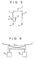
Fig. 5 is a circuit diagram showing the configuration of a phase shift
circuit according to a second embodiment of the present invention;
Fig. 6 is a circuit diagram showing the configuration of a phase shift
circuit according to a fourth embodiment of the present invention;
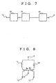
Fig. 7 is a circuit diagram showing the configuration of a phase shifter
according to a fifth embodiment of the present invention;
Fig. 8 is a circuit diagram showing the configuration of a known phase
shift circuit;
Fig. 9 is an equivalent circuit diagram when an FET 6a and an FET 6b
of the known phase shift circuit are made into on-states; and
Fig. 10 is an equivalent circuit diagram when the FET 6a and the FET
6b of the known phase shift circuit are made into off-states.
BEST MODE FOR CARRYING OUT THE INVENTION
Embodiment 1.
Fig. 1 is a view showing the construction of a phase shift circuit
according to a first embodiment of the present invention. 1 designates a
semiconductor substrate, 2 a high frequency signal input/output terminal, 3 a
line, 4 a spiral inductor, 5 an MIM capacitor, 6 an FET, 7 through holes, 8 a
resistor, and 9 a bias terminal. The phase shift circuit shown in Fig. 1 is
monolithically formed on the semiconductor substrate 1.
Fig. 2 is an equivalent circuit diagram of Fig. 1 showing the
configuration of the phase shift circuit according to the first embodiment. The
same or corresponding parts or components as those of Fig. 1 are identified by
the same symbols while omitting overlapping explanations. As new symbols,
10 designates a capacitor corresponding to the MIM capacitor 5, 11 an inductor
corresponding to the spiral inductor 4, and 12 ground corresponding to the
through holes 7.
The FET 6 acts as switches for switching between an on-state and an
off-state. In addition, the bias terminal 9 is connected with a gate electrode of
the FET 6.
Here, when a gate voltage of the same potential as those of a drain
voltage and a source voltage of the FET 6 is applied to the bias terminal 9, the
FET 6 is turned into an on-state, exhibiting resistivity (hereinafter referred to as
on-resistance). On the other hand, when a gate voltage equal to or below a
pinch-off voltage is applied to the bias terminal 9, the FET 6 is turned into an
off-state, exhibiting capacitivity (hereinafter referred to as off-capacitance).
Next, the operation of Fig. 1 is explained by using Fig. 2 that is an
equivalent circuit of Fig. 1.
Fig. 3 shows an equivalent circuit diagram of Fig. 1 when the FET 6 is
in an on-state. 13 is an on-resistance of the FET 6. Here, assuming that the
on-resistance 13 is small enough, the circuit shown in Fig. 3 can be considered
as a parallel LC circuit comprising the capacitor 10 and the inductor 11. Thus,
a signal input from the high frequency signal input/output terminal 2 is reflected
due to a phase rotation generated by the above-mentioned parallel LC circuit,
so that it is output from the high frequency signal input/output terminal 2.
Fig. 4 shows an equivalent circuit diagram of Fig. 1 when the FET 6 is
in an off-state. 14 is an off-capacitance of the FET 6. Here, assuming that
an admittance of the capacitor 10 is small enough, the circuit shown in Fig. 4
can be considered as a series LC circuit comprising the inductor 11 and the off-capacitance
14. Thus, a signal input from the high frequency signal
input/output terminal 2 is reflected due to a phase rotation generated by the
above-mentioned series LC circuit, so that it is output from the high frequency
signal input/output terminal 2.
Therefore, the phase shift circuit of the first embodiment shown in Fig.
1 changes the amount of phase rotation generated upon reflection of the signal
input from the high frequency signal input/output terminal 2 by switching
between the parallel LC circuit and the series LC circuit through the on/off
switching operation of the FET 6.
As described above, according to the phase shift circuit of the first
embodiment, a desired amount of phase shift can be obtained due to the
difference in the amount of phase rotation by setting the inductance of the
inductor 11, the capacitance of the capacitor 10 and the capacitance of the off-capacitance
14 in an appropriate manner. In other words, the circuit can be
formed of the single FET, the inductor and the capacitor, so the number of
FETs can be decreased by one as compared with the prior art, thus making it
possible to reduce the size of the circuit.
Although in the phase shift circuit according to the first embodiment
shown in Fig. 1, the FET 6 is used as a switching element, any form of switch
can be used as long as it has a switching function capable of switching
between an on-state and an off-state. In addition, the phase shift circuit
according to the first embodiment shown in Fig. 1 is monolithically formed on
the semiconductor substrate 1, but a passive element may be formed on a
dielectric substrate and an active element may be formed on a semiconductor
substrate, with both of the substrates being electrically connected with each
other by means of metal wires, gold bumps, etc., thereby to form a phase shift
circuit.
Embodiment 2.
Fig. 5 is a view showing the construction of a phase shift circuit
according to a second embodiment of the present invention. As a new
symbol, 15 designates a resistor. The same or corresponding parts or
components as those of Figs. 1 and 2 are identified by the same symbols while
omitting overlapping explanations. The phase shift circuit according to this
second embodiment has, in Fig. 2 showing the configuration of the phase shift
circuit according to the above-mentioned first embodiment, the resistor 15
connected in parallel with the FET 6.
Next, the operation of the phase shift circuit of the above-mentioned
configuration according to the second embodiment will be explained.
When the FET 6 is in an on-state, the circuit shown in Fig. 5 can be
considered as a parallel LC circuit comprising an inductor 11 and a capacitor
10, similar to the above-mentioned first embodiment. Assuming that an
admittance of the capacitor 10 is small enough when the FET 6 is in an off-state,
the circuit shown in Fig. 5 can be considered as a series LC circuit
comprising the inductor 11 and an off-capacitance 14, similar to the above-mentioned
first embodiment. In this connection, the difference between an
amount of attenuation when the circuit is made to operate as the parallel LC
circuit and an amount of attenuation when the circuit is made to operate as the
series LC circuit is reduced by means of the resistor 15.
As described above, according to the phase shift circuit of the second
embodiment, advantageous effects similar to those of the above-mentioned
first embodiment can be obtained. In addition, by appropriately setting the
resistor 15, it is possible to reduce the difference between the amount of
attenuation when the FET 6 is turned into an on-state to make the circuit
operate as a parallel LC circuit and the amount of attenuation when the FET 6
is turned into an off-state to make the circuit operate as a series LC circuit,
whereby compensation for the level of a high frequency output signal can be
achieved in a simple and easy manner.
Although in the phase shift circuit according to the second embodiment
shown in Fig. 5, the FET 6 is used as a switch, any form of switch can be used
as long as it has a switching function capable of switching between an on-state
and an off state.
In addition, the phase shift circuit according to the second embodiment
shown in Fig. 5 is monolithically formed on the semiconductor substrate 1, but
a passive element may be formed on a dielectric substrate and an active
element may be formed on a semiconductor substrate, with both of the
substrates being electrically connected with each other by means of metal
wires, gold bumps, etc., thereby to form a phase shift circuit.
Embodiment 3.
In the phase shift circuit according to the first embodiment shown in Fig.
2 and the phase shift circuit according to the second embodiment shown in Fig.
5, assuming that the inductance of the inductor 11 is L, the capacitance of the
capacitor 10 is C, the capacitance of the off-capacitance 14 is C1, and the
characteristic impedance of the line is Z0, there is formed a phase shift circuit
that satisfies the following expression (1).
Z0 = (L/C)1/2 = (L/C1)1/2
Next, the operation of the phase shift circuit of the above-mentioned
configuration according to a third embodiment will be explained.
Assuming that the reflected phase of the parallel LC circuit is 1, and
that the reflected phase of the series LC circuit is 2, the amount of phase
shift Φ is represented by the difference between the reflected phases of both
circuits, that is, Φ = 1 - 2. If the differential coefficient of the amount of
phase shift with respect to frequency becomes zero, the amount of phase shift
results in a constant value over all frequencies. That is, the following equation
has only to be satisfied over all the frequencies: dΦ/dω = d(1-2)/dω = 0.
The solution that satisfies this conditional expression is given by expression (1)
above if intermediate expressions are omitted.
When expression (1) above is satisfied, the resonance frequencies of
the series LC circuit and the parallel LC circuit become equal to each other,
because of (L/C)1/2 = (L/C1)1/2. In addition, the series LC circuit is put into a
short-circuited state at the resonance frequency, and hence the reflected
phase is zero. Also, the parallel LC circuit is put into an open state, so the
reflected phase is delayed by 180°.
Therefore, at the resonance frequency, the difference between the
reflected phases of both circuits, i.e., the amount of phase shift, becomes
180° . Furthermore, if expression (1) above is satisfied, the amount of
phase shift becomes a constant value of 180° over all the frequencies.
As described above, according to the phase shift circuit of the third
embodiment, advantageous effects similar to those of the above-mentioned
first or second embodiment can be obtained. Besides, by satisfying
expression (1) above, the amount of phase shift of 180° can be achieved
over a wide frequency range.
Embodiment 4.
Fig. 6 is a view showing the construction of a phase shifter according
to a fourth embodiment of the present invention. 16 designates a high
frequency signal input terminal, 17 a high frequency signal output terminal, 18
a 90° hybrid coupler, and 19a and 19b reflective terminating circuits. The
phase shift circuit according to either of the above-mentioned first through third
embodiments is applied to the reflective terminating circuits 19.
Next, the operation of the phase shifter of the above-mentioned
configuration according to the fourth embodiment will be explained.
A high frequency signal is input from the high frequency signal input
terminal 16 to the 90° hybrid coupler 18. A signal of the same phase as that
of the high frequency signal input to the 90° hybrid coupler 18 is input to the
reflective terminating circuit 19a, and a signal, which is delayed by 90° in
phase, is input to the reflective terminating circuit 19b. The high frequency
signals, differing in phase by 90° from each other, are reflected by the
reflective terminating circuits 19a, 19b, respectively, while generating desired
phase rotations therein.
The reflected high frequency signals are again input to the 90° hybrid
coupler 18. Since the phases of the signals reflected by the reflective
terminating circuits 19a, 19b are mutually different by 180° from each other at
the high frequency signal input terminal 16, no output appears there, and an
output is obtained only at the high frequency signal output terminal 17.
Here, note that the phase shift circuit according to either of the above-mentioned
first through third embodiments is applied to the reflective
terminating circuits 19a, 19b, and by switching the states of the reflective
terminating circuits 19a, 19b at the same time, a desired amount of phase shift
is obtained from the difference between the reflected phases in the respective
states. As a result, the input signal and the output signal are separated from
each other, whereby only the signal reflected by the reflective terminating
circuits 19 can be taken out as an output signal.
As described above, according to the phase shifter of this fourth
embodiment, there can be provided a phase shifter with a one-bit phase shift
which generates, as an output signal, only the signal reflected by the reflective
terminating circuits 19.
Here, note that the phase shifter according to the fourth embodiment
shown in Fig. 6 may be monolithically formed on a semiconductor substrate.
In addition, a passive element and a 90° hybrid coupler may be formed on a
dielectric substrate and an active element may be formed on a semiconductor
substrate, with both of the substrates being electrically connected with each
other by means of metal wires, gold bumps, etc., thereby to form a phase
shifter.
Embodiment 5.
Fig. 7 is a view showing the construction of a phase shifter according
to a fifth embodiment of the present invention. 20 designates a phase shifter
of a one-bit phase shift, and a plurality of phase shifters 20 are connected with
one another in a multistage fashion. The same or corresponding parts or
components as those of Fig. 6 are identified by the same symbols while
omitting overlapping explanations. Here, the phase shifter described in the
above-mentioned fourth embodiment is applied to the phase shifters 20. A
phase shifter unit that operates in multi-bit can be achieved by connecting the
one-bit phase shifters 20 with one another in a multistage fashion.
Here, note that the phase shifter according to the fifth embodiment
shown in Fig. 5 may be monolithically formed on a semiconductor substrate.
Moreover, a passive element and a 90° hybrid coupler may be formed on a
dielectric substrate and an active element may be formed on a semiconductor
substrate, with both substrates being electrically connected with each other
through metal wires, gold bumps, etc., thereby to form a phase shifter.
According to a phase shift circuit of the present invention, the phase
shift circuit includes a capacitor, and a series circuit composed of a switching
element which exhibits capacitivity when it is in an off-state and an inductor
connected in series with this switching element, the series circuit being
connected in parallel with the capacitor. The capacitor and one terminal of the
series circuit are connected with a high frequency signal input/output terminal,
and the other terminal thereof is connected with ground. Thus, by setting the
inductance of the inductor, the capacitance of the capacitor and the
capacitance of the off-capacitance in an appropriate manner, it is possible to
obtain a desired amount of phase shift due to the difference in the amount of
phase rotation. That is, the phase shift circuit can be formed by using the
single switching element, and hence reduction in size of the circuit can be
achieved.
In addition, a resistor is connected in parallel with the switching
element, so that by appropriately setting the resistor, it is possible to reduce
the difference between an amount of attenuation when the switching element
is turned into an on-state to make the circuit operate as a parallel LC circuit
and an amount of attenuation when the switching element is turned into an off-state
to make the circuit operate as a series LC circuit, as a consequence of
which compensation for the level of a high frequency output signal can be
achieved in a simple and easy manner.
Moreover, assuming that the capacitance of the capacitor is C, the
inductance of the inductor is L, and the capacitance of the switching element in
its off-state is C1, the characteristic impedance Z0 of the high frequency signal
input/output terminal satisfies an equation Z0 = (L/C)1/2 = (L/C1)1/2. As a result,
the amount of phase shift can be made to be 180° over a wide frequency
range.
Further, either of the above-mentioned phase shift circuits is connected
with a 90° hybrid coupler having a high frequency signal input terminal and a
high frequency signal output terminal, so that a desired amount of phase shift
can be obtained according to the difference in the reflected phases of the
respective phase shift circuits. Accordingly, it is possible achieve a phase
shifter with a one-bit phase shift which is capable of taking out only the signal
reflected by the phase shift circuits as an output signal by separating a high
frequency input signal and a high frequency output signal from each other.
Furthermore, by mutually connecting the above-mentioned high
frequency signal input terminal and the above-mentioned high frequency signal
output terminal in the above-mentioned phase shifter with each other in a
multistage fashion, it is possible to achieve a phase shifter that operates in
multi-bit.
INDUSTRIAL APPLICABILITY
As described above, according to the present invention, it is possible
to achieve a phase shift circuit and a phase shifter which are small in size and
wide in bandwidth.